Article

Design and Modelling of Metal-Oxide Nanodisk Arrays for Structural Colors and UV-Blocking Functions in Solar Cell Glass Covers

by
Albert Peralta Amores
,
Ajith Padyana Ravishankar
* and
Srinivasan Anand
Department of Applied Physics, School of Engineering Sciences, KTH Royal Institute of Technology, Albanova University Center, Roslagstullsbacken 21, SE-106 91 Stockholm, Sweden
*
Author to whom correspondence should be addressed.
Photonics 2022, 9(5), 273; https://doi.org/10.3390/photonics9050273
Submission received: 4 April 2022 / Revised: 14 April 2022 / Accepted: 16 April 2022 / Published: 19 April 2022
(This article belongs to the Special Issue Advances in Photovoltaic Technologies from Atomic to Device Scale)

Abstract

:
We present a multifunctional structural coloration strategy for solar cell glass covers based on all-dielectric nanoscatterer arrays. Titanium dioxide (TiO2) nanostructures are designed to efficiently scatter in the visible and absorb in the UV region, making them suitable candidates as UV absorptive color coatings. Results from finite difference time domain (FDTD) simulations on a square lattice of TiO2 nanocylinders show that a rich palette in the reflected colors can be obtained by varying the period of the lattice. The reflected colors are narrow-banded, with a typical FWHM ~11–17 nm, leading to a minimal penalty on the amount of transmitted light. This narrow band reflectance is attributed to the interaction of Mie resonances between individual scatterers with their neighbors in the lattice. The color appearance, with viewing angles of ~45°, is maintained for incidence angles up to ~70°. With TiO2 being transparent for a major part of silicon solar cells spectral response (400–1100 nm), a loss of ~4.5–9.2% in the short-circuit current has been estimated in the specified wavelength range, primarily due to the loss of photons in the reflected light. Furthermore, due to the inherent UV-absorption properties of TiO2, the proposed color-cover designs reduce the transmittance of UV radiation (320–400 nm) by up to ~63.70%, potentially preventing the degradation of the encapsulation materials and thus increasing the lifetime expectancy of a solar panel.

1. Introduction

The constant increase in global energy demand has led to an overconsumption of non-renewable resources that are currently primary sources of energy. As a result, the world energy market is slowly moving away from non-renewable energy sources and investing heavily on renewable alternatives such as photovoltaic, hydroelectric, wind and tidal power sources. Although photovoltaic (PV) energy just accounts for a 7% of the global renewable sources, it is gradually dominating the energy market since 2010 [1,2]. A PV module or a solar panel is traditionally installed on a roof top of a building to maximize the exposure of the device to the daylight. Most of the building surfaces are generally inaccessible to install a solar panel. A substantial part of light falling on these surfaces is unharnessed. Building integrated photovoltaics (BIPVs) is an upcoming technological solution that aims to integrate photovoltaic materials directly onto a building surface [3]. BIPVs can be integrated on sidewalls of a building [4], glass windows [5], or building overhangs on which sunlight exposure is considerably high. Aesthetics is a major concern when a building surface is replaced with BIPVs. Color of the building is one such aesthetic factor. Adding color as a functionality to a PV module without compromising its efficiency is challenging. A typical PV module consists of a solar cell with a protective polymer layer called an encapsulant and a glass superstrate to provide mechanical stability. Addition of an absorptive or a reflective color layer above the glass covering will be at the cost of the amount of light reaching the active region of the solar panel. Nonetheless, it is difficult to achieve a wide gamut of colors and at the same time maintain a minimum penalty on the light transmitted through the color layer.
Photonic/plasmonic grating structures, that generate colors by utilizing the photonic band gap or surface plasmon excitations, have been presented to integrate color functionality into PV modules [6,7,8]. However, the relatively wide photonic bandgaps and inherent losses (ohmic) of plasmonic (metallic) structures leads to a higher penalty on PV performance [9]. Moreover, these structures are designed such that the color is generated directly at the active region or very close to the active region. Practically, this would involve processing on top of the solar cell that could potentially lead to diminished performance. Subwavelength dielectric nanostructures can support different types of optical modes such as Mie (electric and magnetic dipoles, quadrupoles, etc.), Fabry–Perot and whispering gallery modes. Given the right conditions, the interaction between the modes can lead to special properties such as perfect reflectance, anti-reflectance, lasing and color generation [10,11,12,13]. Additionally, dielectric nanostructures are not as lossy as the metallic ones and they have been demonstrated to produce highly saturated reflective colors [14,15,16]. The color saturation can be further improved by suppressing multipolar Mie resonance modes at non-resonant wavelengths [13]. The application of Mie resonators to PV cell technologies has been traditionally limited in proposing forward scattering geometries to enhance the coupling of light into the substrate [17]. However, it is possible to generate reflective color in the green spectral region and efficiently forward scatter the rest of the spectra on a silicon PV cell, but with a relative loss of 10% in short-circuit current [18]. The other interesting aspect of Mie resonators is that they can be designed to support higher order modes in the UV spectral region. With the right choice of material, the modes can get absorbed inside the resonator. This is especially useful in the context of longevity of the encapsulant layer in a PV module. An encapsulant is a layer sandwiched between a solar cell and a protective glass superstrate cover. It provides electrical insulation, acts as an index matching interface, and protects the solar cells from environmentally induced damages [19]. In recent years, ethylene vinyl acetate (EVA) has been the most commonly used encapsulation material for solar cells [20]. It is well known that with UV photobleaching EVAs significantly degrade in terms of optical transmittance, adhesion, and shear strength [21]. The acetic acid produced during the EVA degradation process corrodes the solder bonds and the electrical contacts, increasing the leakage current through the encapsulant [22].
In this study, a design strategy is provided to combine the two functionalities, reflective structural color in the visible spectral region and light absorption in the UV spectral region, in a dielectric Mie resonator array. We propose the use of metal-oxide semiconductors which exhibit the following characteristics: a moderately high refractive index (RI)~2, high transparency in the visible-NIR spectral range and efficient absorption the UV [23]. These properties make metal-oxides (ex TiO2, ZnO, etc.) an excellent choice to achieve structural coloring and UV-blocking functions as well as high transparency. TiO2 nanoresonator arrays have been demonstrated to generate structural colors that display extended color saturation and hue, including polarization sensitive colors [13,16,24,25]. Nevertheless, such approaches require multi-dielectric stacked layers greatly reducing the fabrication feasibility and thus, the implementation of such technologies. However, there are technologies such as nanoimprint lithography or colloidal lithography that may solve the scalability issue of these designs [26]. Recently, TiO2 nanostructures have been fabricated using colloidal lithography to show broadband anti-reflection in solar cells [27]. In this work, using finite difference time domain (FDTD) simulations, we show that TiO2 disk resonators arrays exhibit narrowband reflective colors that can be tuned by both the size of the resonator and the array period. The influence of embedding the resonators inside a transparent low-index media (ex. silica or encapsulant material) on properties of the reflective colors is investigated. In addition, through a set of figures of merit (FOMs), we quantify the penalty on the efficiency of the solar cell as well as the UV blocking strength of the color layer.

2. Simulation Setup

All the simulations have been carried out using commercial Finite Difference Time Domain (FDTD) software, Lumerical [28]. A TFSF (Total Field Scattered Field) source was incident normally on a single TiO2 disk resonator placed in air (RI = 1). The RI for TiO2 has been taken from the Palik database and its extinction coefficient, in the wavelength range of 320–400 nm, was obtained from Sarkar et al.’s data [29]. The scattered light was collected by the field monitors kept outside of the TFSF region. To elucidate the Mie resonances contributing to the scattering, multipole decomposition was computed using the electric fields induced inside the resonator due to the external light source [30]. The decomposition of the resonator quantifies the contribution of electric and magnetic multipole moments (dipole, quadrupole, etc.) to the total scattering cross-section. For TiO2 nanoarray simulations periodic boundary conditions were used in x, y boundaries, and the light was an incident in the z-direction.

3. Results and Discussion

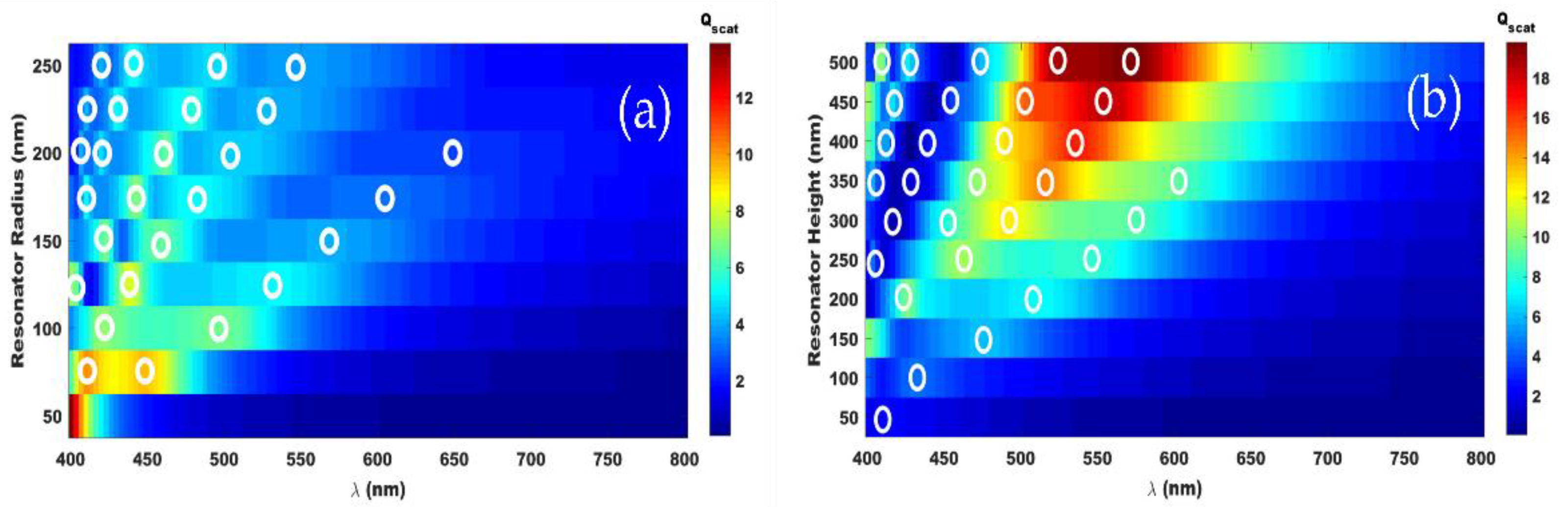
3.1. Scattering Cross-Section (SCS) of TiO2 Nanodisk Resonator

Figure 1a shows the multipole decomposition of the scattering cross-section (SCS) from an isolated disk resonator with radius (r) of 110 nm and height (h) of 200 nm in the visible spectra (400–700 nm). The scattering peaks appear between 400 to 450 nm or in the blue region of the spectral sensitivity of the human eye. Although the scattering responses of resonators of different geometries (cylindrical/disk, spherical and cubic) show slight differences, the spectral peaks are in the same regions (Supplementary info Figure S1). At the nanoscale, disk resonators are more convenient to fabricate compared to spherical or cubic resonators. Therefore, the results presented in this work are based on the studies conducted only on disk resonators. Resonances in the forward (FS) or backward (BS) scattering occur when electric dipole (ED) and magnetic dipole (MD) satisfy Kerker conditions. FS and BS were computed for a TiO2 disk of radius 110 nm and height 200 nm is presented in Figure 1b, along with the FS/BS ratio that shows resonance close to the wavelength region where ED and MD resonances spectrally overlap [31].
Studies have shown that the aspect ratio of a disk resonator influence not only the response of the multipoles but also the forward and the backward scattering properties [32,33]. Therefore, in order to tailor the backward scattering from an array of disk resonators it is essential to study the effect of radius and height of a disk resonator on the scattering properties. Normalized SCS of TiO2 disk resonators as a function of the disk radius and height is presented in Figure 2. With the increasing radius of the disk, the multipole peaks broaden and red-shift (Figure 2a). Increasing the dimension of a resonator results in a larger fraction of the fields confined within the resonator, thus red-shifting the resonant wavelength [34]. Though the red-shift and broadening of the multipole resonances are also observed as a function of the height of a disk (Figure 2b), quantitatively, the SCS increases with the increasing height, unlike the previous case (radius dependent SCS). It should be noted that the geometrical cross-section/normalization factor (πr2) depends on the radii, but not on the height of the disk resonator. The higher order modes (EQ and MQ) occur for larger radii (>125 nm) at shorter wavelengths and their resonances are narrow compared to the lower order modes. Specifically, the modes in the range of 320–400 nm (UV region) can also get absorbed within the TiO2 resonators. The multipole decomposition shows that the ED and the MD resonances are in the same spectral region for the disks of radius above 60 nm. Therefore, one can expect Kerker conditions to be satisfied within this spectral region for these disks, leading to an efficient forward or backward scattering.
Once the resonances supported in isolated TiO2 nanodisks were established, the scattering response of the resonator in the presence of SiO2 substrate (RI = 1.46) was investigated (Figures S2 and S3). We observe that this situation leads to a reduced red-shifting of resonance with increasing radius/height, attributed to resonance–substrate coupling, when the resonator dimensions are increased. The confinement of a fraction of the near-fields within the substrate reduces the fraction of field confined within the high-index resonator resulting in a reduced red-shift, but a substantial resonance broadening. For a TiO2 resonator of a radius 110 nm and a height of 220 nm placed on SiO2 substrate, the SCS resonance profile is very similar to that of a resonator placed in air. Therefore, the multipole mode positions in the visible region does not differ significantly due to the presence of a silica substrate. This is possibly due to a lower RI of the substrate compared to the disk resonator. The resonance peaks in FS/BS ratio, on the other hand, blue shift and additional peaks appear due to symmetry breaking [33].

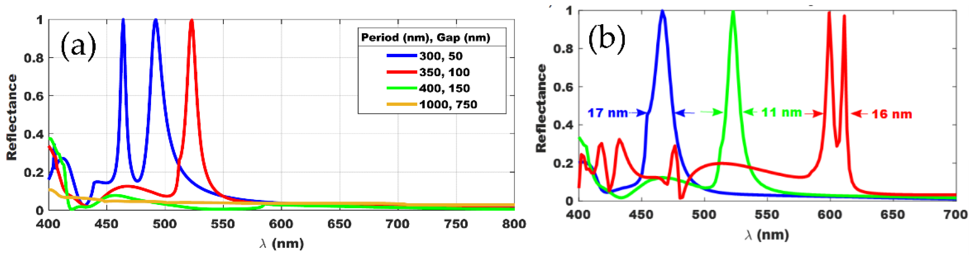
3.2. Reflectance from TiO2 Nanodisk Array

The optical responses from Mie resonators in arrays change dramatically compared to the isolated case. An array of resonators may behave as an effective index medium or a photonic crystal or Mie scatterers depending on the gap between any two neighboring resonators in the lattice [35]. Sometimes a specific arrangement of a resonator lattice leads to exotic optical properties such as Fano resonances. A narrow reflectance is observed due to the interference between the directly reflected light and a dipole mode of the resonator. Such properties have been adopted to generate structural colors and polarization sensitive narrow bandwidth color pixels [24,36]. Our analysis show that a range of narrowband reflective colors arise (Figure 3a) when the TiO2 resonators are arranged in a square lattice with lattice constants of ~300–400 nm and gap distances of ~20–120 nm. The narrowband reflectance not only improves the saturation of the color, but also reduces the penalty on the transmittance. To maintain high reflectance and narrow peak in the reflected colors, some optimization of the disk size and the lattice constants are necessary. The height of the TiO2 disk resonators was fixed at 200 nm as the dipolar response can be tuned effectively throughout the visible spectra via variation of the disk radius between 90 and 190 nm. A typical narrowband (FWHM~14 nm) R, G, B reflective colors obtained from TiO2 disks on silica substrate is shown in Figure 3b. The XYZ tristimulus and the sRGB values were computed for the reflectance spectra. The range of colors that can be generated using different combinations of the period, and the gap between the resonators are presented as a color palette in Figure 4a. The colors range from violet to pink, with green dominating the overall palette. The colors are also presented as xy points on the CIE 1931 chromaticity map (Figure 4b). The excitation of higher order resonant modes at shorter wavelengths hinders the color saturation preventing a monochromatic reflectance. Such an effect is particularly detrimental for long-wavelength engineered resonances making it difficult to produce a true red structural color.
We find that the reflected colors are sensitive to the polarization of the incoming light that is an incident that is off-normal or at an angle. For an incident of p-polarized light, the resonator array (r = 125 nm, h = 200 nm and period = 350 nm) does not produce a reflectance peak for any incidence angles larger than 10º, as shown in Figure 5a. Whereas, for the case of s-polarized light, the reflectance peak not only exists for all the incidence angles up to 70° (Figure 5b), but also the spectral peak position blue shifts only by about 30 nm. A similar observation has been made in the case of TiO2 metasurfaces wherein the reflectance spectra is highly angle-sensitive for an incident p-polarized light and the reflected intensity drastically reduces for the off-normal angle of incidences [16]. This suggests that the reflected color is mostly s-polarized light for the off-normal configurations. However, in this scenario the transmitted p-polarized light can be absorbed by the solar cell.
The reflectance profile from the resonator array for an incident of unpolarized light can be computed as the mean between the perpendicular polarizations. The color palette shown in Figure 5c displays angle sensitivity of the reflected color for an incident of unpolarized, s- and p-polarized light. The color palette due to an incident of unpolarized light does not differ drastically with the incidence angle. Though the reflectance peak vanishes for incidence angles above 10° in the case of p-polarized light, a certain amount of reflectance, specifically in the blue spectral region still contributes to the overall color. This is especially apparent in the incidence angle ranging from 20°–50°. As a result, a slight variation in the reflected color is observed for the incident of unpolarized light. The suppression of reflectance in the case of p-polarized light is an added advantage as it reduces the penalty on the transmitted light that can be absorbed by the solar cell.
Next, we investigate the structural colors in the context of protective layers. The resonator arrays, when used as a color covering over solar cell devices, are prone to external contamination that could possibly change the RI dramatically at the air-scatterer interface or provoke irreversible damage to the structures. Additionally, the presence of adsorbed radicals on the TiO2 surface due to its inherent photocatalytic properties could lead to undesired photochemical reactions at the PV cell vicinities. Polymer coatings are commonly used to protect such nanostructured surfaces. The coating reduces the RI contrast between the resonator and its surrounding. This modifies the reflection profile of the resonator array and consequently changing the color palette. If the contrast between the resonator RI and the surrounding RI is high enough, the perceived change in color will be limited. Therefore, we simulate the TiO2 resonators by embedding them inside a thick silica layer (RI = 1.46). Although we have chosen silica as the protective layer, RI of encapsulants is also in the similar range. Figure 6 demonstrates the variation in the perceived color when the resonators are fully embedded inside silica layer. It is evident from Figure 6a that the colors from the embedded resonators show a wider palette compared to the unembedded ones (Figure 4a). Furthermore, the resonances in the embedded structures are much sharper (Figure S4). Here, the colors range from dark blue to light magenta with a near equal distribution of shades of blue and green in the palette.

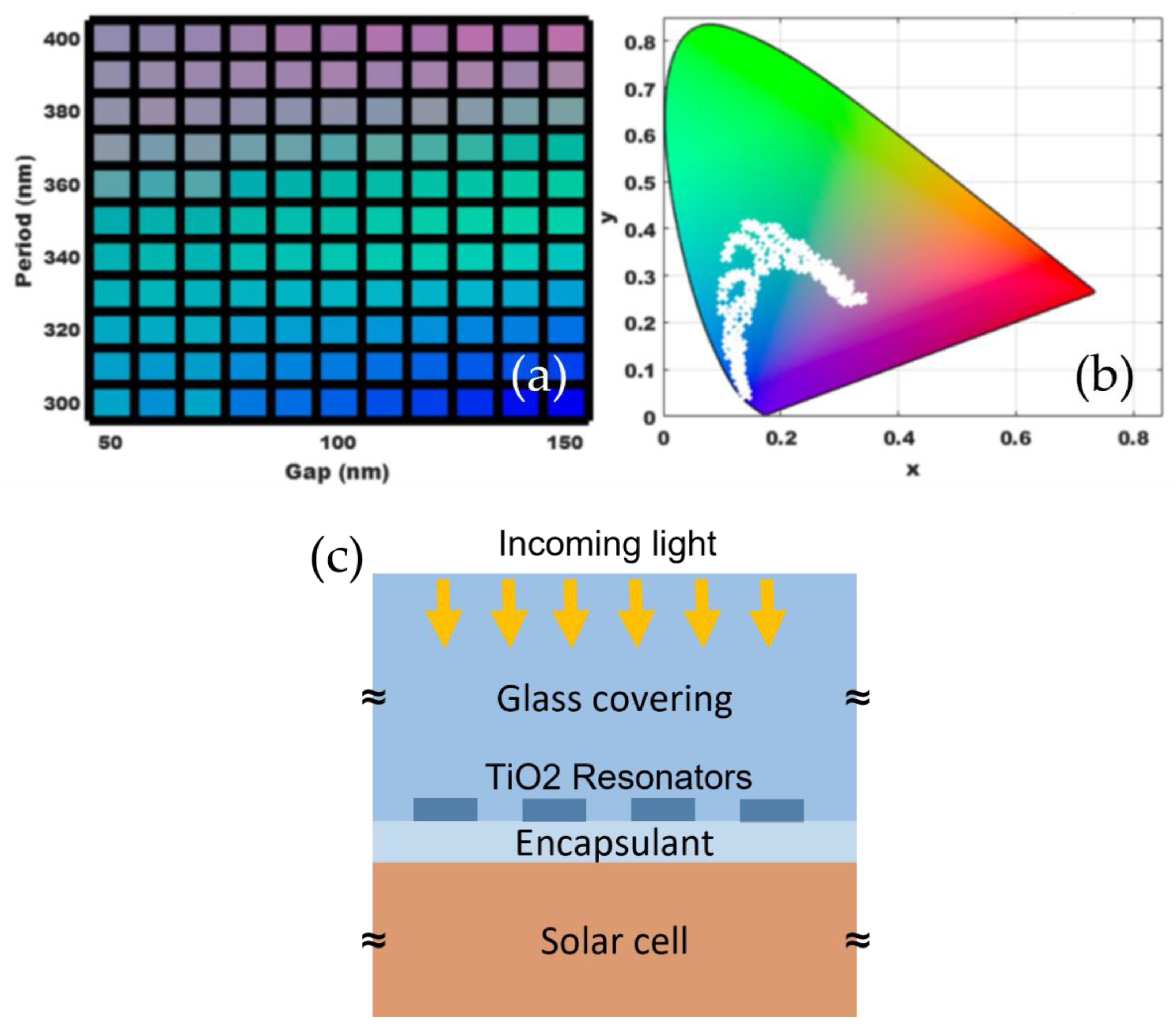
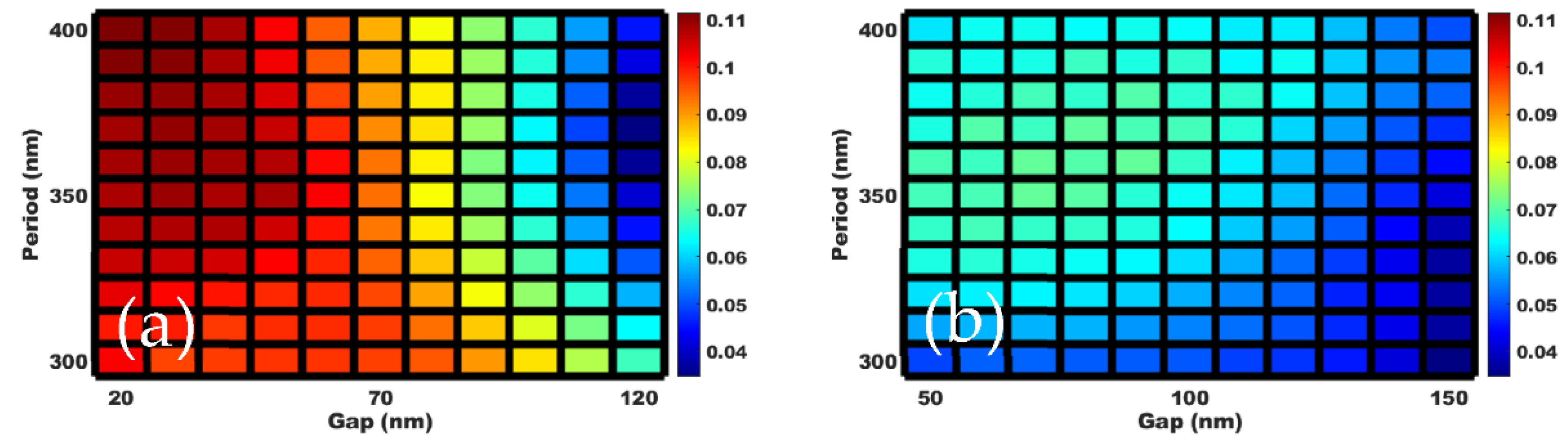
3.3. Assessment of TiO2 Resonator Array as Efficient Color and UV Absorber Coating

To assess the performance of the TiO2 resonator array as both an efficient color coating with minimum penalty on transmittance and a UV absorber coating, we introduce two FOMs. The FOMs were calculated for spectra obtained at a normal incidence of light. The first FOM—FoMPenalty (Equation (1))—estimates the short-circuit current loss in a silicon PV cell due to the addition of the colored cover. This is computed from the following relation.
F o M P e n a l t y = 1 400 1200 ϕ A M   1.5   G ( λ ) · I Q E · ( 1 R ) · d λ 400 1200 ϕ A M   1.5   G ( λ ) · I Q E · d λ
where, ϕ A M   1.5   G is the AM 1.5 G-173 solar irradiance spectral data obtained from NREL, IQE the internal quantum efficiency of a solar cell, and R is the reflectance obtained from the simulations. It is assumed that each photon reaching the solar cell excites an electron–hole pair and there are no carrier recombination losses. There is always a loss in the number of photons reaching the solar cell due to the reflected light from the nanodisk array. Here reflectance is the penalty parameter that needs to be minimized. This implies narrower the bandwidth of the reflected color lesser is the penalty on transmittance. Note that reflectance penalty is taken only from the first interface (i.e., air-TiO2-SiO2 interface) and not from the Si-SiO2 interface. The spectral information on ϕ A M   1.5   G and I Q E is provided in the supplementary information (Figure S6). We have calculated FoMPenalty in the wavelength range of 400–1200 nm as the irradiance of AM 1.5 peaks in the visible wavelengths but drops significantly in the UV region. Furthermore, the efficiency of a Si solar cell is the highest in the considered wavelength range.
The calculated solar cell performance penalty, due to the color layer, for different array period and gap between the resonators is shown as a color tile of FoMPenalty in Figure 7. The upper and lower limits for the penalty of the structures on silica (Figure 7a) are estimated to be 11.15% (r = 190 nm and P = 400 nm) and 3.46% (r = 125 nm and P =370 nm), respectively. Specifically, the penalty is higher for the lower gap (~50–100 nm) and larger periods (~350–400 nm) and the penalty gradually reduces in the resonator arrays with larger gap distances. The mean penalty determined is ~8%. Here, we note for comparison that the typical penalty for a plain glass is ~3–4%. The embedded structures exhibit a performance penalty between ~3.5% (r = 75 nm and P = 300 nm) and ~7 % (r = 145 nm and P = 360 nm) with a mean penalty of ~5% and thus improves the overall performance of the device (Figure 7b). Like the non-embedded structures, the embedded structures exhibit a similar trend of increased penalty when the gap between the resonators is lesser, and the period is larger.
The second FOM—FoMTotal-UV (Equation (2))—estimates the UV blocking at the color layer in the spectral region of 320–400 nm. Here, the UV blocking happens in two ways. First is by backscattering of the UV radiation that manifests as the total reflectance (R) and the other is the total absorption (A) inside the TiO2 resonator. Therefore, we use total transmittance (T = 1 − R − A) as the FOM parameter in 320–400 nm spectral range, as it includes contributions from both, reflectance, and absorbance. This figure of merit, termed as FOMTotal-UV, is given by,
F o M T o t a l - U V = 1 320 400 ϕ A M   1.5   G ( λ ) · T · d λ 320 400 ϕ A M   1.5   G ( λ ) · d λ
The calculated UV blocking ability of the color layer, for different array periods and gaps between the resonators is shown as a color tile of FOMTotal-UV in Figure 8. For the resonator array on silica substrate (Figure 8a), the highest UV blocking FOM is estimated to be ~60% (r = 135 nm, h = 200 nm, P = 340 nm) and the lowest is ~33% (r = 90 nm, h = 200 nm, P = 300 nm). Array design with period of around ~330–350 nm and resonator gap of ~80–120 nm gives the best FOMTotal-UV. For the embedded resonator arrays (Figure 8b) the FOMTotal-UV is higher than the non-embedded arrays and it is around ~64%. The FOMTotal-UV is higher for the array designs that have period ~300–350 nm and gap distances of ~50–100 nm. For practical applications, it is important to estimate nanodisk (or array) geometry that gives best FoMs in both transmission penalty and UV absorption. There are several parameters associated with TiO2 disk arrays that will affect the FoMs—a consequence of variation in reflectance spectra with tuning of these parameters. For example, modifying array period not only shifts the position of reflectance peak, but also changes the reflected intensity. Changing the size and shape of individual nanodisks might support higher order modes affecting both the reflected color and UV absorption within the nanodisk. Furthermore, materials other than TiO2, such as ZnO, AZO, etc., can be explored to control or modify reflectance and absorptance profiles. Therefore, to evaluate a design for the best possible FoMs requires extensive multi-parameter optimizations that is beyond the scope of this study.

4. Conclusions

In conclusion, the study was aimed at providing a design strategy for a multifunctional color layer composed of metal oxide resonator arrays. Such color layers are highly desired in building integrated PVs. The presented designs of TiO2 nanodisk resonator array function both as color panels above a solar cell and as a UV blocking layer. Individual disk resonators were simulated using FDTD method to elucidate possible Mie mode resonances and the dependence of the resonances on the physical parameters (disk height and radius) of the disk. It is found that a TiO2 resonator array placed on a SiO2 substrate leads to a narrow band (~11–17 nm) reflective color that is tunable by changing array period. The optimal period and resonator sizes were determined to generate red (R), green (G) and blue (B) reflective colors. The angle sensitivity of the reflected s-polarized light is minimal, but the reflected p-polarized light drops in intensity for off-normal incidences. Therefore, if unpolarized light (ambient sunlight) is an incident on the color layer where only s-polarized light is utilized to produce the color, whereas p-polarized is transmitted into the substrate, subsequently reaching the solar cell beneath. Due to narrow spectral profile of the reflective colors, penalty on the transmission of light through the color layer is minimal. Embedding the resonators in silica medium affected the color response. The color palette was in fact broader ranging from dark blue to light pink. We formulated two figures of merit that quantify short-circuit current loss in the solar cell and the UV blocking due to the color layer. UV blocking is crucial in the context of the degradation of encapsulant that is sandwiched between the solar cell and the glass cover. In the case of non-embedded arrays, the penalty on solar cell performance is the lowest in the cases of larger gaps (~140–150 nm) and larger period (~350–380 nm) and the UV blocking is most efficient for the array designs with period ~330–350 nm and resonator gap distances of ~80–120 nm. Embedding the array structures improves both the solar cell performance and UV absorption FOM, especially in the array design region where non-embedded has the highest penalty on the solar cell performance. Robust and scalable fabrication technologies need to be explored to realize such multifunctional color arrays on solar cells including ways to embed the resonator arrays inside a medium, such as glass, without compromising on the integrity of the array design.

Supplementary Materials

The following supporting information can be downloaded at: https://www.mdpi.com/article/10.3390/photonics9050273/s1, Figures S1–S6.

Author Contributions

Conceptualization, A.P.A., A.P.R. and S.A.; Investigation, A.P.A., A.P.R. and S.A.; Methodology, A.P.A. and A.P.R.; Software, A.P.A. and A.P.R.; Formal analysis, A.P.A., A.P.R. and S.A.; Writing—original draft, A.P.A. and A.P.R.; Writing—review and editing A.P.A., A.P.R. and S.A.; Supervision, A.P.R. and S.A.; Project administration, S.A.; Funding acquisition, S.A. All authors have read and agreed to the published version of the manuscript.

Funding

This research was funded by the Swedish Research Council—Vetenskapsrådet, grant number 2019-05321, and by the Swedish Energy Agency—Energimyndigheten, grant number 2018-07073.

Institutional Review Board Statement

Not applicable.

Informed Consent Statement

Not applicable.

Data Availability Statement

The data presented in this study are available on request from the corresponding author.

Conflicts of Interest

The authors declare that they have no known competing financial interests or personal relationships that could have appeared to influence the work reported in this paper.

References

  1. IRENA. Renewable Energy Statistics 2019; The International Renewable Energy Agency: Abu Dhabi, United Arab Emirates, 2019; ISBN 978-92-9260-137-9. [Google Scholar]
  2. IRENA. Off-Grid Renewable Energy Solutions: Global and Regional Status and Trends; The International Renewable Energy Agency: Abu Dhabi, United Arab Emirates, 2018; ISBN 978-92-9260-076-1. [Google Scholar]
  3. Ballif, C.; Perret-Aebi, L.E.; Lufkin, S.; Rey, E. Integrated Thinking for Photovoltaics in Buildings. Nat. Energy 2018, 3, 438–442. [Google Scholar] [CrossRef]
  4. Heinstein, P.; Ballif, C.; Perret-Aebi, L.E. Building Integrated Photovoltaics (BIPV): Review, Potentials, Barriers and Myths. Green 2013, 3, 125–156. [Google Scholar] [CrossRef]
  5. Traverse, C.J.; Pandey, R.; Barr, M.C.; Lunt, R.R. Emergence of Highly Transparent Photovoltaics for Distributed Applications. Nat. Energy 2017, 2, 849–860. [Google Scholar] [CrossRef]
  6. Yu, W.; Shen, L.; Jia, X.; Liu, Y.; Guo, W.; Ruan, S. Improved Color Rendering Index of Low Band Gap Semi-Transparent Polymer Solar Cells Using One-Dimensional Photonic Crystals. RSC Adv. 2015, 5, 54638–54644. [Google Scholar] [CrossRef]
  7. Park, H.J.; Xu, T.; Lee, J.Y.; Ledbetter, A.; Guo, L.J. Photonic Color Filters Integrated with Organic Solar Cells for Energy Harvesting. ACS Nano 2011, 5, 7055–7060. [Google Scholar] [CrossRef]
  8. Lee, K.T.; Jang, J.Y.; Zhang, J.; Yang, S.M.; Park, S.; Park, H.J. Highly Efficient Colored Perovskite Solar Cells Integrated with Ultrathin Subwavelength Plasmonic Nanoresonators. Sci. Rep. 2017, 7, 10640. [Google Scholar] [CrossRef] [Green Version]
  9. Kristensen, A.; Yang, J.K.W.; Bozhevolnyi, S.I.; Link, S.; Nordlander, P.; Halas, N.J.; Mortensen, N.A. Plasmonic Colour Generation. Nat. Rev. Mater. 2016, 2, 16088. [Google Scholar] [CrossRef]
  10. Moitra, P.; Slovick, B.A.; Li, W.; Kravchencko, I.I.; Briggs, D.P.; Krishnamurthy, S.; Valentine, J. Large-Scale All-Dielectric Metamaterial Perfect Reflectors. ACS Photonics 2015, 2, 692–698. [Google Scholar] [CrossRef]
  11. Cordaro, A.; Van De Groep, J.; Raza, S.; Pecora, E.F.; Priolo, F.; Brongersma, M.L. Antireflection High-Index Metasurfaces Combining Mie and Fabry-Pérot Resonances. ACS Photonics 2019, 6, 453–459. [Google Scholar] [CrossRef] [Green Version]
  12. Gargas, D.J.; Moore, M.C.; Ni, A.; Chang, S.W.; Zhang, Z.; Chuang, S.L.; Yang, P. Whispering Gallery Mode Lasing from Zinc Oxide Hexagonal Nanodisks. ACS Nano 2010, 4, 3270–3276. [Google Scholar] [CrossRef]
  13. Yang, B.; Liu, W.; Li, Z.; Cheng, H.; Choi, D.Y.; Chen, S.; Tian, J. Ultrahighly Saturated Structural Colors Enhanced by Multipolar-Modulated Metasurfaces. Nano Lett. 2019, 19, 4221–4228. [Google Scholar] [CrossRef] [PubMed]
  14. Dong, Z.; Ho, J.; Yu, Y.F.; Fu, Y.H.; Paniagua-Dominguez, R.; Wang, S.; Kuznetsov, A.I.; Yang, J.K.W. Printing beyond SRGB Color Gamut by Mimicking Silicon Nanostructures in Free-Space. Nano Lett. 2017, 17, 7620–7628. [Google Scholar] [CrossRef] [PubMed]
  15. Frolov, A.Y.; Verellen, N.; Li, J.; Zheng, X.; Paddubrouskaya, H.; Denkova, D.; Shcherbakov, M.R.; Vandenbosch, G.A.E.; Panov, V.I.; Van Dorpe, P.; et al. Near-Field Mapping of Optical Fabry-Perot Modes in All-Dielectric Nanoantennas. Nano Lett. 2017, 17, 7629–7637. [Google Scholar] [CrossRef]
  16. Sun, S.; Zhou, Z.; Duan, Z.; Xiao, S.; Song, Q. All-Dielectric Full-Color Printing with TiO2 Metasurfaces. ACS Nano 2017, 11, 4445–4452. [Google Scholar] [CrossRef]
  17. Spinelli, P.; Verschuuren, M.A.; Polman, A. Broadband Omnidirectional Antireflection Coating Based on Subwavelength Surface Mie Resonators. Nat. Commun. 2012, 3, 692. [Google Scholar] [CrossRef] [PubMed] [Green Version]
  18. Neder, V.; Luxembourg, S.L.; Polman, A. Efficient Colored Silicon Solar Modules Using Integrated Resonant Dielectric Nanoscatterers. Appl. Phys. Lett. 2017, 111, 073902. [Google Scholar] [CrossRef]
  19. Kempe, M. Encapsulant Materials for PV Modules. Photovolt. Sol. Energy 2017, 478–490. [Google Scholar] [CrossRef]
  20. Peike, C.; Peike, C.; Hädrich, I.; Weiß, K.; Dürr, I.; Ise, F. Overview of PV Module Encapsulation Materials. Photovolt. Int. 2013, 19, 85–92. [Google Scholar]
  21. Czanderna, A.W.; Pern, F.J. Encapsulation of PV Modules Using Ethylene Vinyl Acetate Copolymer as a Pottant: A Critical Review. Sol. Energy Mater. Sol. Cells 1996, 43, 101–181. [Google Scholar] [CrossRef]
  22. Kempe, M.D.; Jorgensen, G.J.; Terwilliger, K.M.; McMahon, T.J.; Kennedy, C.E.; Borek, T.T. Acetic Acid Production and Glass Transition Concerns with Ethylene-Vinyl Acetate Used in Photovoltaic Devices. Sol. Energy Mater. Sol. Cells 2007, 91, 315–329. [Google Scholar] [CrossRef]
  23. Johansson, W.; Peralta, A.; Jonson, B.; Anand, S.; Österlund, L.; Karlsson, S. Transparent TiO2 and ZnO Thin Films on Glass for UV Protection of PV Modules. Front. Mater. 2019, 6, 259. [Google Scholar] [CrossRef]
  24. Yang, B.; Liu, W.; Li, Z.; Cheng, H.; Chen, S.; Tian, J. Polarization-Sensitive Structural Colors with Hue-and-Saturation Tuning Based on All-Dielectric Nanopixels. Adv. Opt. Mater. 2018, 6, 1–8. [Google Scholar] [CrossRef]
  25. Shapturenka, P.; Birkholz, F.; Zakaria, N.I.; DenBaars, S.P.; Gordon, M.J. Quasiordered, Subwavelength TiO 2 Hole Arrays with Tunable, Omnidirectional Color Response. J. Vac. Sci. Technol. A 2020, 38, 053403. [Google Scholar] [CrossRef]
  26. Sanchez-Sobrado, O.; Mendes, M.J.; Haque, S.; Mateus, T.; Araujo, A.; Aguas, H.; Fortunato, E.; Martins, R. Colloidal-Lithographed TiO2 Photonic Nanostructures for Solar Cell Light Trapping. J. Mater. Chem. C 2017, 5, 6852–6861. [Google Scholar] [CrossRef]
  27. Visser, D.; Chen, D.Y.; Désières, Y.; Ravishankar, A.P.; Anand, S. Embossed Mie Resonator Arrays Composed of Compacted TiO2 Nanoparticles for Broadband Anti-Reflection in Solar Cells. Sci. Rep. 2020, 10, 12527. [Google Scholar] [CrossRef]
  28. Lumerical Solutions FDTD. Available online: https://www.lumerical.com/products/fdtd/ (accessed on 6 April 2022).
  29. Sarkar, S.; Gupta, V.; Kumar, M.; Schubert, J.; Probst, P.T.; Joseph, J.; König, T.A.F. Hybridized Guided-Mode Resonances via Colloidal Plasmonic Self-Assembled Grating. ACS Appl. Mater. Interfaces 2019, 11, 13752–13760. [Google Scholar] [CrossRef] [Green Version]
  30. Alaee, R.; Rockstuhl, C.; Fernandez-Corbaton, I. An Electromagnetic Multipole Expansion beyond the Long-Wavelength Approximation. Opt. Commun. 2018, 407, 17–21. [Google Scholar] [CrossRef] [Green Version]
  31. Alaee, R.; Filter, R.; Lehr, D.; Lederer, F.; Rockstuhl, C. A Generalized Kerker Condition for Highly Directive Nanoantennas. Opt. Lett. 2015, 40, 2645. [Google Scholar] [CrossRef]
  32. Staude, I.; Miroshnichenko, A.E.; Decker, M.; Fofang, N.T.; Liu, S.; Gonzales, E.; Dominguez, J.; Luk, T.S.; Neshev, D.N.; Brener, I.; et al. Tailoring Directional Scattering through Magnetic and Electric Resonances in Subwavelength Silicon Nanodisks. ACS Nano 2013, 7, 7824–7832. [Google Scholar] [CrossRef]
  33. Butakov, N.A.; Schuller, J.A. Designing Multipolar Resonances in Dielectric Metamaterials. Sci. Rep. 2016, 6, 38487. [Google Scholar] [CrossRef] [Green Version]
  34. van de Groep, J.; Polman, A. Designing Dielectric Resonators on Substrates: Combining Magnetic and Electric Resonances. Opt. Express 2013, 21, 26285. [Google Scholar] [CrossRef] [PubMed]
  35. Rybin, M.V.; Filonov, D.S.; Samusev, K.B.; Belov, P.A.; Kivshar, Y.S.; Limonov, M.F. Phase Diagram for the Transition from Photonic Crystals to Dielectric Metamaterials. Nat. Commun. 2015, 6, 10102. [Google Scholar] [CrossRef] [PubMed]
  36. Shen, Y.; Rinnerbauer, V.; Wang, I.; Stelmakh, V.; Joannopoulos, J.D.; Soljačić, M. Structural Colors from Fano Resonances. ACS Photonics 2015, 2, 27–32. [Google Scholar] [CrossRef]
Figure 1. (a) Multipole decomposition of the scattering cross-section (SCS) of a single TiO2 resonator of radius 110 nm and height 200 nm placed in air. (b) Forward (red) and backward (blue) scattering profile of the resonator. A resonance in the FS/BS ratio (green) can be seen very close to 550 nm where ED and MD spectrally overlap (black dashed line in Figure 1a).
Photonics 09 00273 g001
Figure 2. Normalized scattering cross-section (SCS) of a single TiO2 resonator, placed in air, (a) as a function of disk radius at a constant height of 200 nm and (b) as a function of disk height at a constant radius of 110 nm. The SCS was normalized with the geometrical cross-section (πr2) of the disk. The white circles represent resonance peaks of ED, MD, and other higher order multipole moments.
Photonics 09 00273 g002
Figure 3. (a) Variation in the reflectance from a TiO2 disk resonator (radius = 200 nm, height = 125 nm) array with changing period (or with changing gap between the neighboring resonators). (b) Red (R), green (G) and blue (B) reflectance profiles generated in a TiO2 disk resonator array. Periodicities chosen to generate R, G, B reflectance colors were 400, 350 and 300 nm, respectively and the corresponding disk radii were 190, 125 and 95 nm. The reflectance peaks are narrow, resulting in a minimum penalty in the transmittance.
Photonics 09 00273 g003
Figure 4. (a) Color palette generated from TiO2 disk resonators (on silica substrate) of height 200 nm for different combinations of array period and gaps. (b) Corresponding positions of the colors on the CIE 1931 chromaticity diagram. (c) A schematic describing the TiO2 resonator array on the silica glass layer above an encapsulated layer on top of a solar cell. Note that, in the simulations, glass covering is considered as a semi-infinite substrate. In this case, the light is incident from the air (n = 1) medium.
Photonics 09 00273 g004
Figure 5. Reflectance spectra from a square array of period 350 nm consisting of TiO2 disk resonators (on silica substrate) of radius 120 nm and of height 200 nm for the incident (a) s-polarized light and (b) p-polarized light. (c) Variation in the color palette for different incidence angles of unpolarized, s- and p-polarized light.
Photonics 09 00273 g005
Figure 6. (a) Color palette generated from TiO2 disk resonators (embedded in silica layer) of height 200 nm for different combinations of array period and gaps. (b) Corresponding positions of the colors on the CIE 1931 chromaticity diagram. (c) A schematic describing TiO2 resonator array on top of encapsulated of a solar cell and embedded within a glass covering. Note that, in the simulations, the refractive of the medium around the TiO2 resonators is assumed to be the same as that of silica layer (n = 1.46), as the refractive indices of glass covering and the encapsulant are similar. The light is the incident form of the silica glass (n = 1.46) medium.
Photonics 09 00273 g006
Figure 7. The calculated FoMPenalty on the loss of short-circuit current due to the color layer above a solar cell for varying period and gap of the TiO2 resonator array, when (a) the resonator array is placed on a silica substrate and (b) the resonator array is embedded inside a silica medium.
Photonics 09 00273 g007
Figure 8. The calculated FoM_Total on UV blocking due to the color layer above a solar cell for a varying period and gap of the TiO2 resonator array, when (a) the resonator array is placed on a silica substrate and (b) the resonator array is embedded inside a silica medium.
Photonics 09 00273 g008
Publisher’s Note: MDPI stays neutral with regard to jurisdictional claims in published maps and institutional affiliations.

