Article

Study of Single Event Burnout Mechanism in GaN Power Devices Using Femtosecond Pulsed Laser

1
National Space Science Center, Chinese Academy of Sciences, Beijing 100190, China
2
School of Astronomy and Space Science, University of Chinese Academy of Sciences, Beijing 100049, China
*
Author to whom correspondence should be addressed.
Photonics 2022, 9(4), 270; https://doi.org/10.3390/photonics9040270
Submission received: 6 March 2022 / Revised: 30 March 2022 / Accepted: 15 April 2022 / Published: 18 April 2022

Abstract

:
Single event burnout (SEB) is a great threat to gallium nitride (GaN) power devices for aerospace applications. This paper is dedicated to the investigation of the SEB mechanism in a GaN power device using a femtosecond pulsed laser. In the test, the SEB of a commercial p-GaN power device was triggered by a focused laser beam with a wavelength of 620 nm, and the irradiation-sensitive area of the devices was identified. We observed that the damage modes were consistent with the results of heavy ion experiments. The vertical breakdown of the drain is proposed as the dominant mechanism of SEB. We also provide a schematic representation of the leakage path formation using the electrical data obtained following laser-induced SEB. This study provides an important reference for consideration of device reliability and application prospects.

1. Introduction

Single event burnout (SEB), induced by high-energy ionizing particles, is a vital reliability concern for electronic power devices used in aerospace applications; the resulting catastrophic failures make it impossible to guarantee power system performance in the space radiation environment. To determine the critical factors affecting SEB, the test device has typically been evaluated by accelerated particle beams, such as heavy ions [1,2,3]. However, the absence of focusing capability makes it difficult to apply ion beams to systematic investigation of SEB with high spatial resolution, and the operation is relatively expensive [4]. Pulsed lasers have played a powerful role in SEB research of silicon (Si) power devices as a more convenient and affordable tool [5,6,7]. Because of its fast response and finely tunable energy, pulsed-laser testing can be used to quickly determine the safe operating area, detect sensitive areas and learn much more about the test device [6,7]. In addition, femtosecond pulsed lasers have recently begun to be used in SEB research into wide bandgap semiconductor devices, such as silicon carbide (SiC) devices [8,9].
Another high melting point wide bandgap semiconductor, gallium nitride (GaN), has a higher breakdown electric field and faster electron migration rate than Si, so that it constitutes an excellent material for the manufacture of low energy consumption, radiation-resistant power devices [10,11]. Specifically, normally-off GaN power devices offer great advantages and potential for space and aerospace power applications. In previous studies [12,13,14,15], heavy ion data for GaN power devices showing SEB responses and brief exploration of the destruction have been reported. These studies have confirmed that when SEB occurs in a device, its electrical properties change, and single event transient (SET) current can be observed during an irradiation run. The damage mode of SEB has also been studied involving observation of the connection between the source and drain directly on the device surface; a vulnerable area is located between the gate and the drain exiting by a short-circuit path; a vertical breakdown of the drain occurs at high voltage, with a short-circuit path to the substrate. Although some research has been carried out on the SEB generation mechanism of GaN power devices, damage exploration has mainly focused on direct observation, using tools such as the scanning electron microscope (SEM) and the emission microscope (EMMI), while a quantitative description of the main factors is lacking. There are also studies of radiation effects in GaN using pulsed lasers. Khachatrian, A. et al. used pulsed lasers for the first time to study the SET mechanism of the GaN high electron mobility transistor (HEMT) via two-photon absorption (TPA) [16]; Roche, N. J. et al. discussed the dependence of a GaN diode device current response on the laser wavelength [17]; Ngom, C. et al. used femtosecond pulsed lasers incident on GaN power devices from the backside, discussing possible absorption mechanisms of femtosecond pulsed lasers in devices and the phenomenon of surface destructive events [18,19]. These studies have mainly focused on verifying the feasibility of radiation tests on GaN power devices, but lack sufficient exploration and interpretation in terms of SEB.
In this paper, we report on the first use of a femtosecond pulsed laser to study the SEB mechanism in GaN power devices. A laser test method is described, and the efficiency of the laser energy is calculated. Next, a normally-off GaN HEMT power device was scanned using a femtosecond pulsed laser by varying the incident laser energy and the device drain bias voltage until SEB occurred. During the process, we obtained information about changes in the electrical properties and detected burnout sensitive areas of the device. SEM was used to evaluate the microscopic failure of the destroyed device. Finally, the irradiated device was electrically tested to analyze the SEB mechanism. The same SEB damage modes were observed using the pulsed laser as in the heavy ion experiment. Analysis of the laser irradiated data is performed to determine the dominant features of SEB and the propagation path of the leakage current in the device.

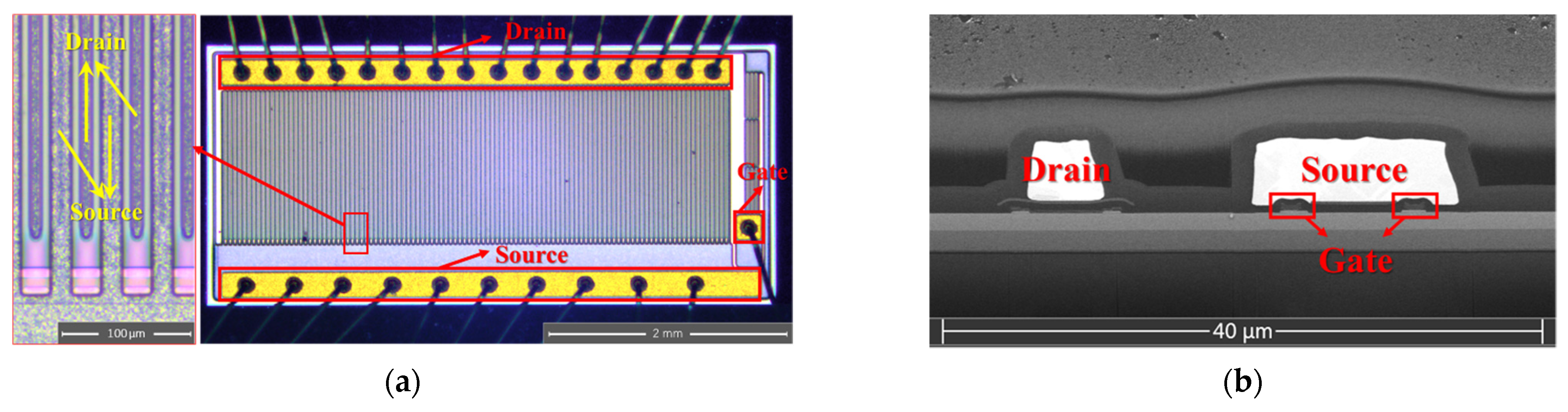
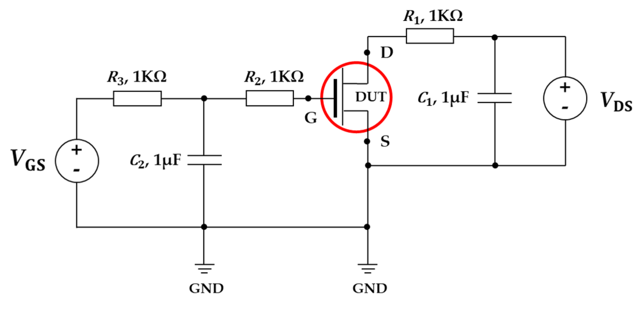
2. Test Device and Circuit

The test device used in this study is a normally-off GaN HEMT power device belonging to the Panasonic PGA26 series, which is a hybrid drain-gate injection transistor (HD-GIT) with a drain-source threshold voltage of 600 V. Figure 1 shows the device surface and cross-sectional view. The structure consists of a substrate (Si), a nucleation layer, a GaN buffer layer, an AlGaN barrier layer, a metal layer and a Si3N4 passivation layer [see Figure 3]. By adding additional p-GaN to the gate and drain regions, holes can be injected to increase the threshold voltage and suppress current collapse at drain voltages of up to 800 V with high reliability [20]. In addition, the substrate of the device is in conductive contact with the back metal, and it can be grounded together with the source in use [21].
The complete test circuit for this device is provided in Figure 2. An RC network is used to ensure that the current in the drain path is limited during the test process, and to prevent failure extension of the circuit threatening experimental safety due to excessive current when SEB occurs. The input power supply is filtered to stabilize the fluctuation values of the output current, so that changes in the electrical properties of the device could be better obtained.

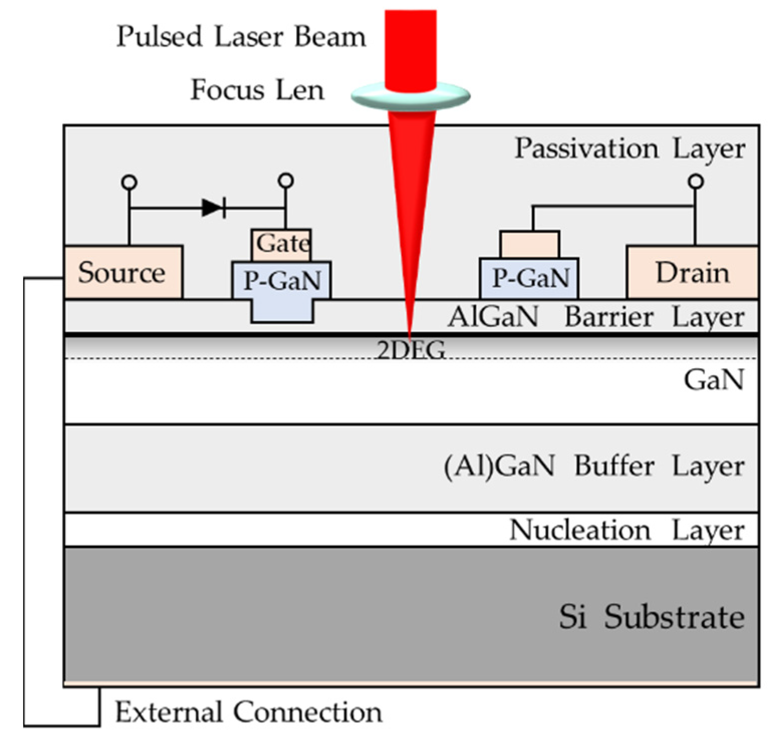
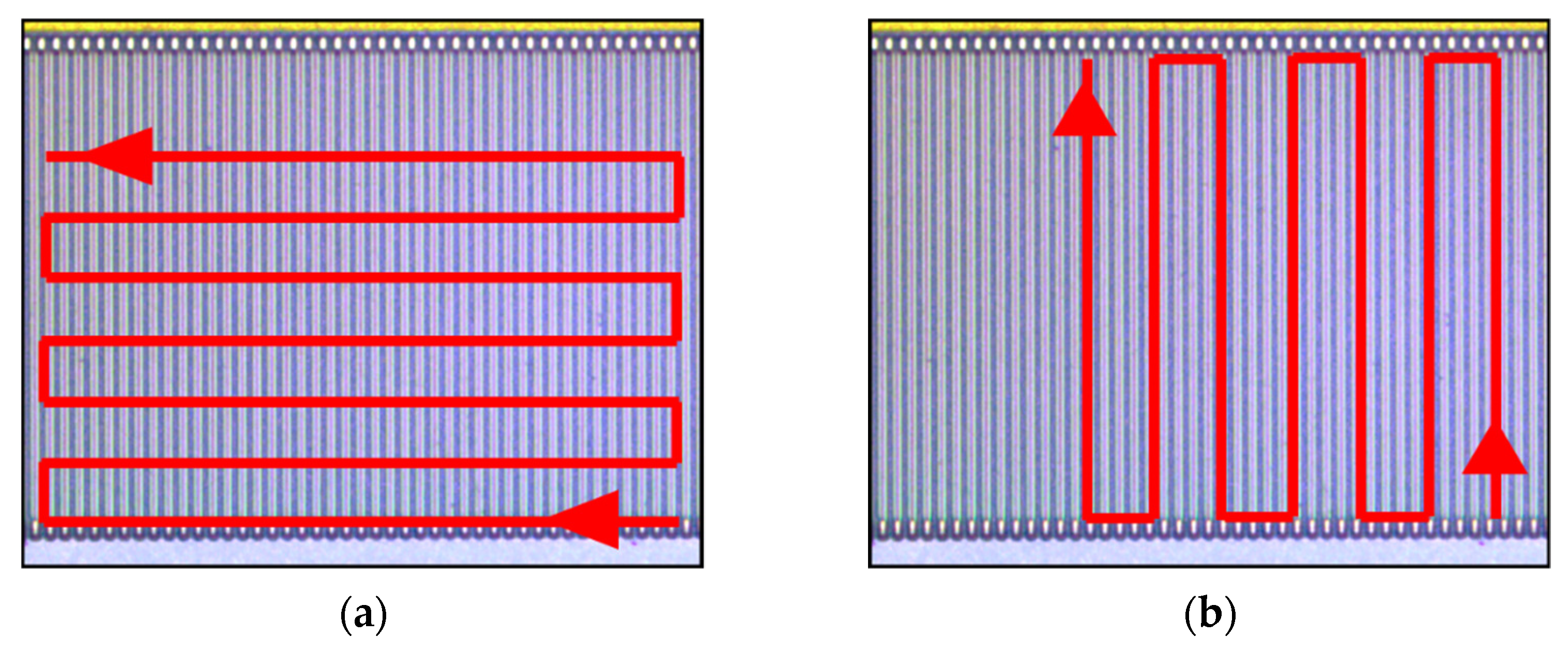
3. Pulsed Laser Test Method

The back of the GaN HEMT power device is completely covered with metal electrodes. For laser testing, the front-side package of the device should be removed, and the pulsed laser is incident from the front side, as shown in Figure 3. When conducting pulsed laser experiments, the laser beam is focused through the dielectric layer in the active region around 2DEG of the GaN layer to generate photoelectric interaction [13,16,19]. When the converted charge of the effective laser energy exceeds the withstand threshold, SEB of the device occurs.
Figure 3. Schematic diagram of the pulsed laser incident on the device from the front side.
Photonics 09 00270 g003
When using pulsed lasers for SEB experiments on GaN power devices, some critical factors need to be determined to ensure laser penetration depth and energy utilization.
The first is the laser wavelength based on the two-photon absorption (TPA) mechanism. TPA means the absorption of two photons simultaneously at high laser intensities to produce a single electron-hole pair, while only acting significantly near the focus of the beam. The increase in beam size in the transmission path makes the laser intensity insufficient to produce TPA, which offers better spatial resolution and longer penetration depth than the single-photon absorption (SPA) mechanism in GaN devices. In this paper, the wavelength of the pulsed laser chosen for the test is 620 nm, and its photon energy can reach 2 eV. The GaN bandgap is 3.4 eV and the energy of two photons of the laser light is greater than the difference between the two energy levels, so that TPA can occur in the active region.
In addition, the interaction of the device materials with the laser is essential in the laser energy transfer process. It should be determined whether the material generates optical losses due to its own absorption effects. The laser is incident from the front side, passing through the passivation layer and the barrier layer in sequence to reach the active region of the GaN layer. The Si3N4 bandgap is 5.1 eV, so the passivation layer does not absorb laser light at 620 nm and the laser energy is barely lost. The thickness of the AlGaN layer is within 100 nm. The thin thickness and wide bandgap allow the laser beam to easily pass through the barrier layer. Therefore, the reduction in absorption by each layer can be ignored for the effective laser energy, and the main influencing factor concerns the interface reflectivity between the layers. Since the thickness of the dielectric layers in the test device is not comparable to the laser wavelength, the interference influence caused by etalon effects is not considered. The effective laser energy in the active region of the device passing through the transmission process can be calculated by Formula (1).
E eff = ( 1 R 1 ) ( 1 R 2 ) ( 1 R 3 ) E 0
Eeff is the effective laser energy in the active region, R1 is the passivation layer reflectivity, R2 is the reflectivity of the interface between the passivation layer and the barrier layer, R3 is the reflectivity of the interface between the barrier layer and the buffer layer, and E0 is the incident laser energy. Except for the passivation layer on the surface of the device, the interface reflectivity should be determined by the materials on both sides of it when the laser light enters. The Fresnel formula can be used to correct the parameters that are needed.
R = ( n 1 n 2 n 1 + n 2 ) 2
R is the interfacial reflectivity, and n1 and n2 are the refractive indices of the different interface side materials. When the laser wavelength is 620 nm, the refractive indices of Si3N4 and GaN are 2.04 and 2.31, respectively [22]. Typically, the refractive index of AlGaN decreases as the Al content increases, but the Al content of AlGaN layers in commercial GaN power devices is commonly kept confidential. Under this optical condition, the refractive index of AlGaN ranges from 2 to 2.32 with variation in Al content [23]. Applying these refractive indexes in the Fresnel equation and the laser transmission process, we obtain an effective laser energy rate of 87.83–88.14%. The Al content has little influence on the effective laser energy, and the pulsed laser energy was well utilized in the test.

4. Experimental Results and Discussion

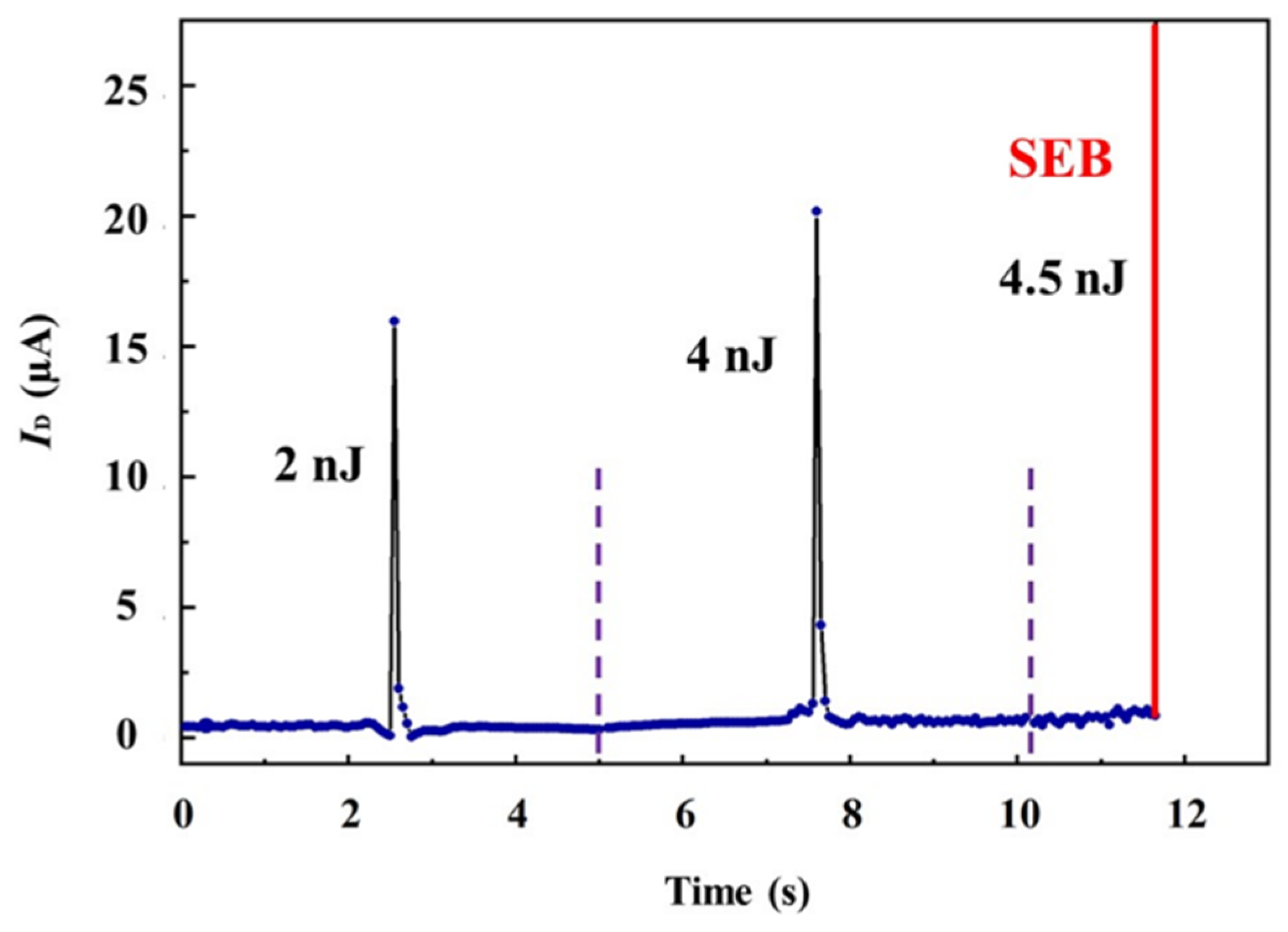
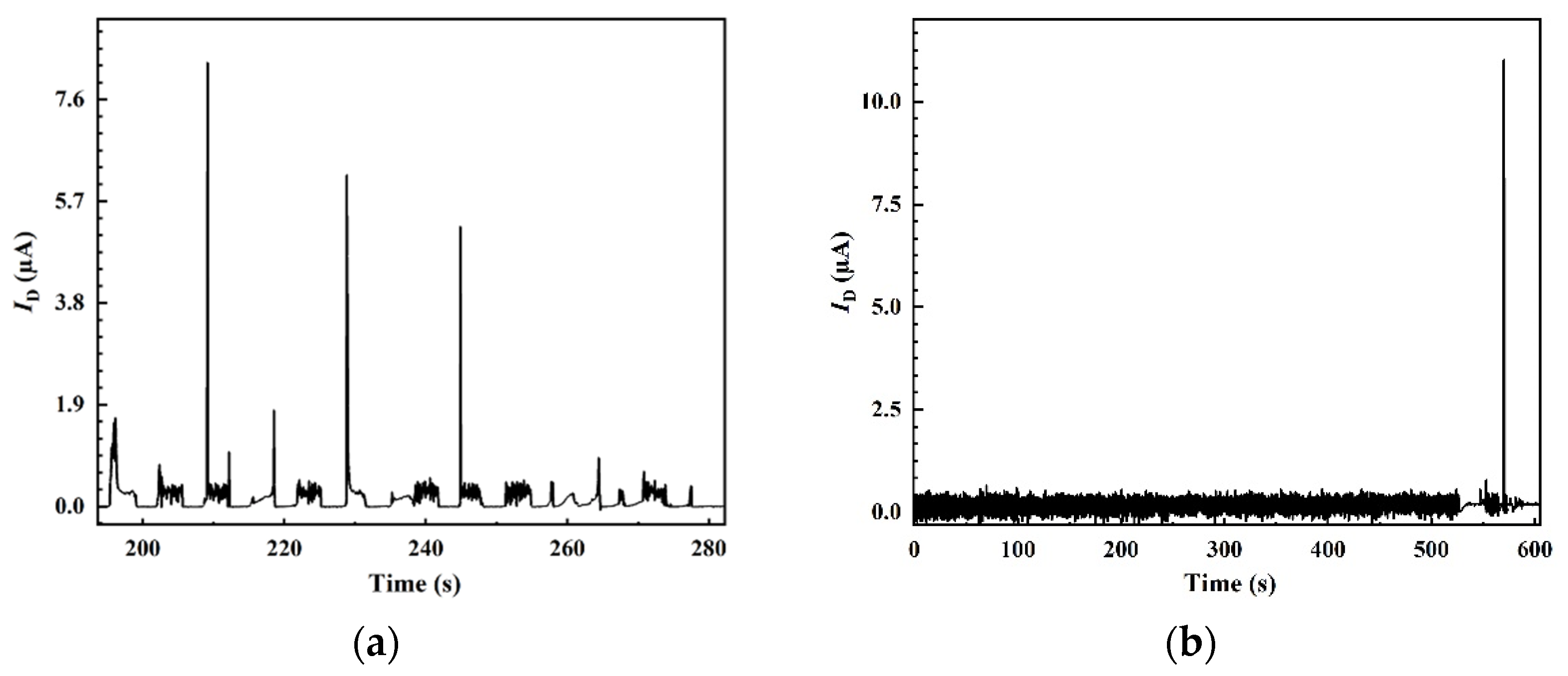
4.1. Pulsed Laser Test

The femtosecond pulsed laser used in this study has a pulse width of 35 fs and a single pulse energy frequency of 5000 Hz. The device was scanned by laser light, the scanning movement rate was 5000 µm/s, and the diameter of the focused spot was about 1 µm.
In the test, the value of the drain current ID is observed to determine whether the device electrical performance is abnormal and the burnout sensitive areas. When the gate-source voltage VGS = 0 V, the device is turned off. The drain-source voltage VDS is set to 500 V. As shown in Figure 4, current transient changes are observed when the laser scans to the irradiation-sensitive areas of the device, and the change amplitude of ID increases as the laser energy increases at 2 nJ and 4 nJ. When the laser energy is up to 4.5 nJ, SEB occurs.
The current change depends on the effective energy deposition in the active region at the sensitive areas. The stronger the incident energy, the more photons are available for TPA, and the more electron-hole pairs will be generated in the active region, which in turn leads to an increase in the device current. When the maximum current that the device can withstand is exceeded, SEB occurs. The current change before burnout is consistent with the heavy ion experimental phenomenon [12].
When the device is scanned, as shown in Figure 5a, current transient changes appear regularly [see Figure 6a]. This indicates that the device is sensitive at a certain structural location. When the device is scanned, as shown in Figure 5b, the laser performs a unit structure test of the device. A larger current transient occurs when the laser scans to a certain drain edge [see Figure 6b], which is the sensitive area. More accumulated charges are generated by the continuous irradiation of the laser to the sensitive area. The scans are performed over the full chip, and the step size in the x and y directions are the length and width of the device surface, respectively.

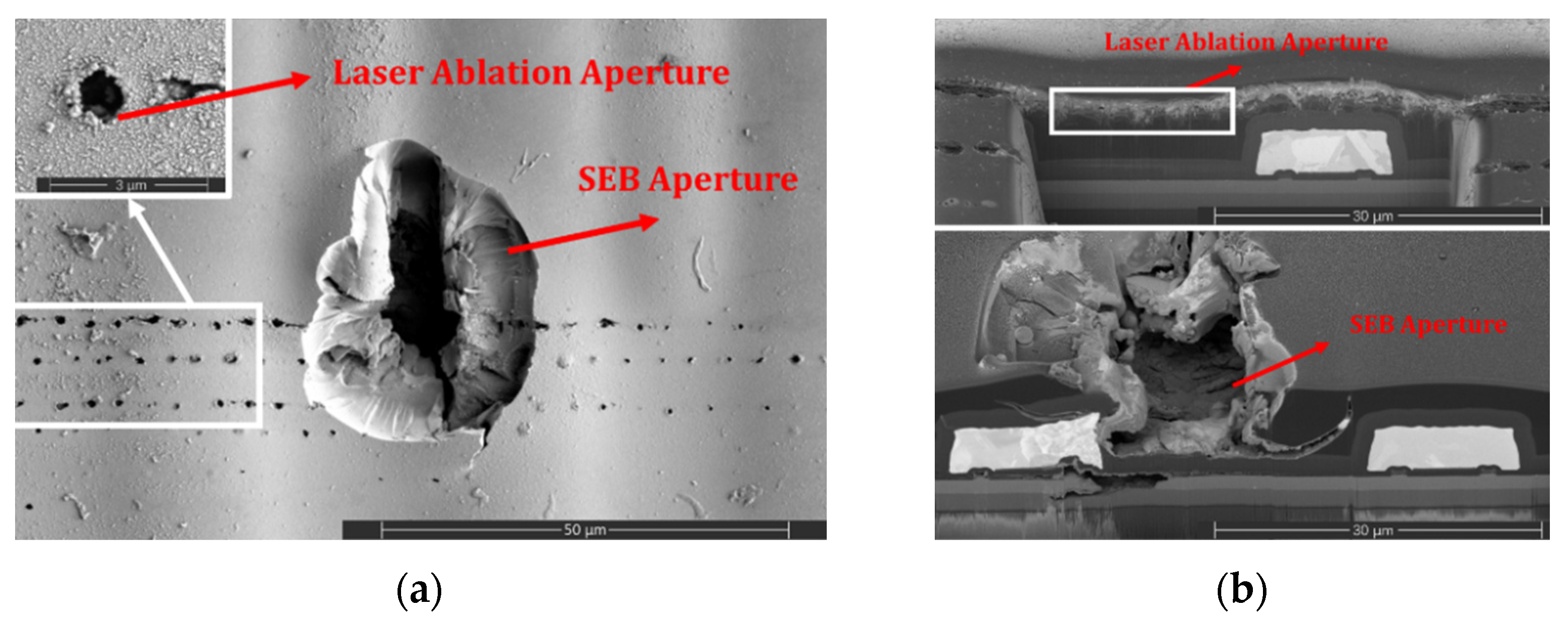
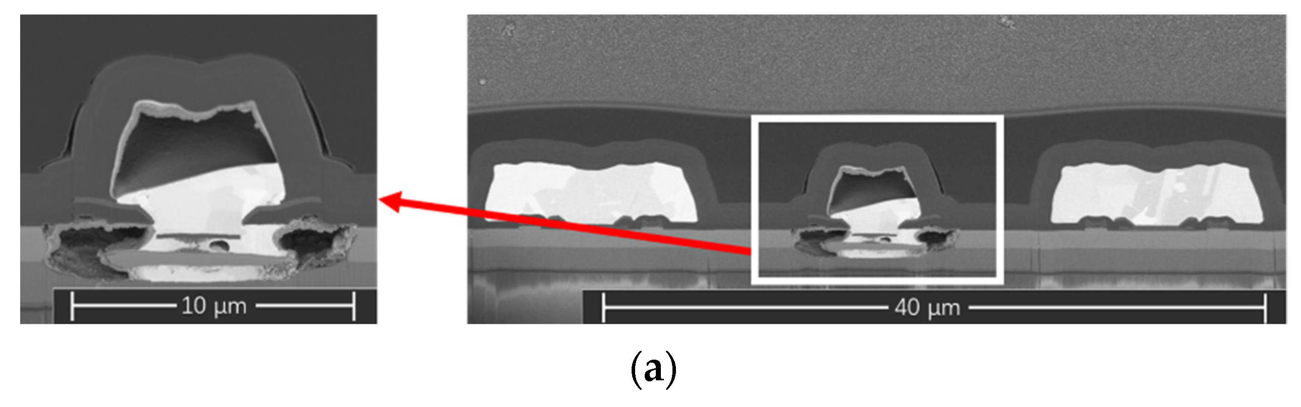
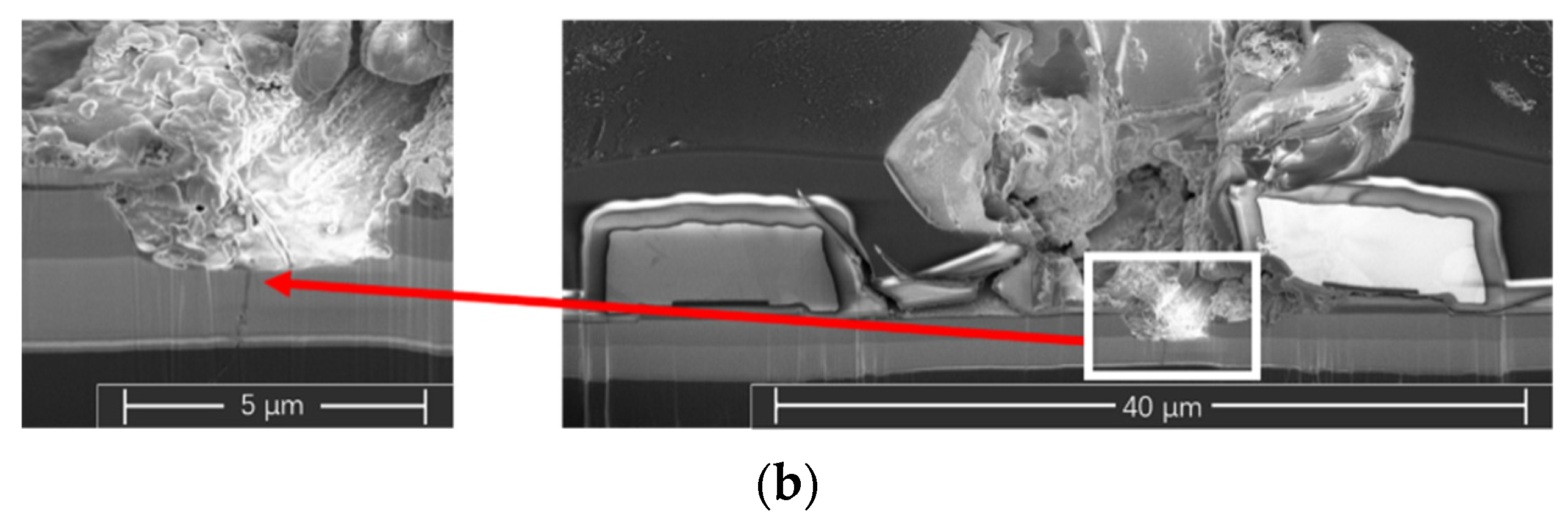
4.2. SEM Verification

SEM was used to perform microscopic failure analysis of the device to identify its burnout sensitivity areas and cause of burnout. Since SEB was induced by the pulsed laser, the damage due to laser thermal accumulation ablation should be excluded first. As shown in Figure 7, the laser ablation aperture plane size within 1.5 µm in diameter and 4 µm in longitudinal depth only produces damage to the passivation layer; while the SEB aperture plane size is up to about 30 µm and longitudinal burnout damages the GaN layer with a depth of more than 10 µm, directly affecting the layer structure. The difference between the two apertures phenomenon is obvious, so the failure caused by laser thermal ablation is excluded in the study.
Figure 8 indicates that the drain is more severely damaged than other regions, and there are more fracture voids at this more sensitive location. During the laser scanning process, current transients are more likely to appear at the edge of the drain. The testing result is consistent with the SEM microscopic observation. Zhang, R. et al. demonstrated that the internal electric field intensity of HD-GIT GaN HEMT power devices is higher at the p-GaN near the drain than other locations [24]. When laser photons hit the drain region, TPA collides and ionizes to generate electron-hole pairs, which increases the number of carriers in the originally high electric field in this region, leading to critical overvoltage transients and transient currents in the drain. Although conventional GaN HEMT devices are almost incapable of avalanche, the p-GaN structure retains some avalanche capability with holes injected from the heterojunction layer. At high VDS, when photons penetrate into the p-GaN vertical region with high electric field [25], continuous impact ionization and avalanche may occur, so that the local internal voltage can instantly exceed the withstand capacity and trigger extremely high current, resulting in vertical breakdown failure of the device [see Figure 8b]. Figure 9 reveals the leakage path between the drain, the gate and the source in the lateral direction after burnout. The rupture damage is not only distributed in the direction of the heterojunction, but also extends to the buffer layer, which may add to the possibility of a leakage path. These findings verify the observation results of the heavy ion experiments from a microscopic perspective.

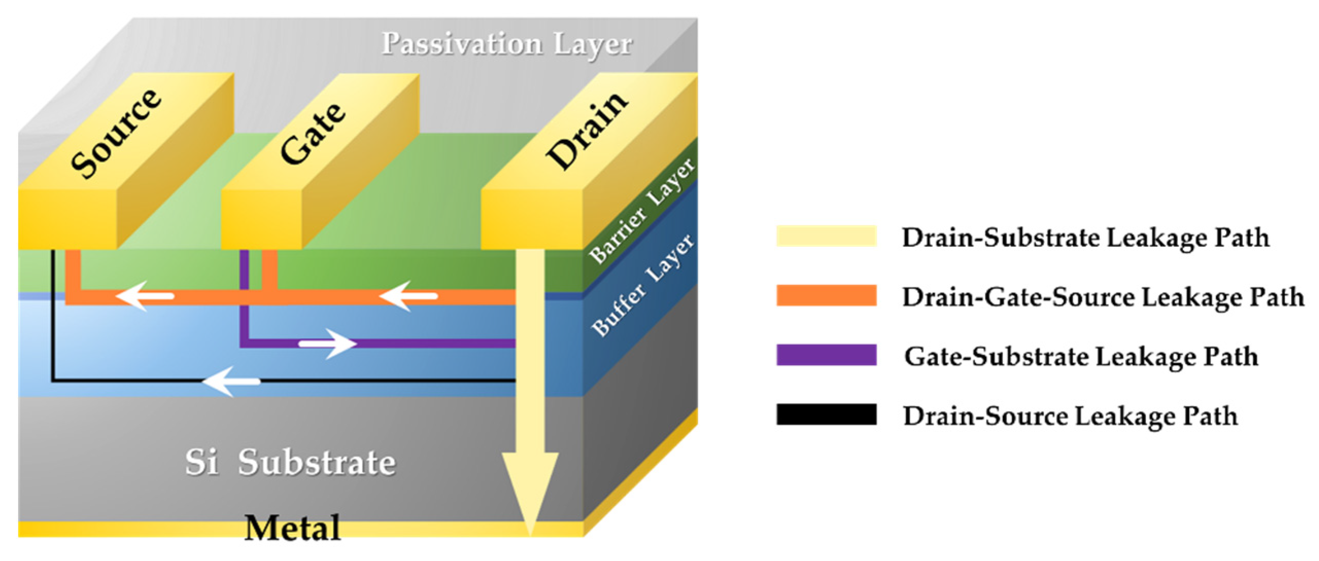
4.3. SEB Mechanism Analysis

We have demonstrated that the laser-induced SEB formation and damage mode of the GaN power device are consistent with the heavy ion results. In addition, the changes in the electrical properties after irradiation were monitored to analyze the SEB mechanism, including the main factors affecting it. Figure 10 shows the electrical properties of the device under different conditions, where New 0 represents a brand new device, Failed 1 represents a SEB device after irradiation, and Failed 2 represents the SEB device with the source-substrate connection line between cut off.
The electrical properties of the device changes greatly before and after irradiation. As shown in Figure 10 New 0, when the VGS is less than 1.5 V or even reversely turned on, the unirradiated new device has essentially no ID and the device is in the off state. The device is in a stable on state at a VGS above 1.5 V. However, as shown in Figure 10 Failed 1, the gate of the irradiated failed device loses its control function. The ID remains almost unchanged and slightly less than the normal new device on state current at the same VDS, regardless of the VGS [see Figure 10a]. Moreover, the IG magnitude is related to VGS and is independent of the positive and negative voltages about the gate [see Figure 10b]. The gate of the unirradiated new device should truncate the conductive channel 2DEG in the off state, so there is a short-circuit path between the destroyed drain and source in the irradiated failed device, and the leakage path is not controlled by the gate. The new device has almost no current when the gate and the source are grounded or reverse voltage is applied between them. However, as shown in Figure 10b, Failed 1 current appears between the gate and the source in the burnout device. IG is out of control: when VGS is reverse biased, IG is the reverse current; when VGS is forward biased, IG is the forward current. The flow direction of IG is consistent with the direction of the applied voltage, which means that there is also a leakage path between the gate and the source at this time. The gate-source is also shorted.
In order to determine the main factors of SEB, the wires connecting the source and the substrate of the failed device are cut to allow the direct test of the drain-substrate current. Figure 10a Failed 1 suggests the ID is 18.93 mA after SEB occurrence. However, the current between the drain and the substrate [see Figure 10a Failed 2] is measured within 15.30 mA after cutting the source-substrate wires, accounting for the domination. There is a large leakage current path penetrating from drain to substrate. Compared with the SEM observations, the electrical property data can confirm that the vertical path located between the drain and the substrate is the most dominant cause of damage under high voltage and irradiation. Figure 10b Failed 2 indicates the reverse current appears between the gate and the substrate when both of them are grounded, which is against common sense. So, we can conclude that there is current flowing from the energized drain to the grounded gate. As the gate voltage increases, the reverse current gradually decreases until the gate-substrate current disappears when the gate-substrate voltage is 5 V. This phenomenon suggests that there is also a leakage path between the gate and the substrate.
Combined with SEM verification, the vertical breakdown of the drain is the most primitive and dominant. Figure 8 indicates great damage appearing in the drain region while the other areas are intact. Following the initial breakdown, the high leakage current increases the energy loss of the device. When the energy deposition is greater than a certain threshold, it will damage the GaN ordered atomic crystal lattice, which leads to melting of the surrounding material, rapid cooling, recrystallization, generation of amorphous material, and production of a high concentration of defects immediately. The presence of a high concentration of defects in the AlGaN barrier layer increases the electric field above the barrier, which facilitates the tunneling and impact ionization processes, increasing the lateral leakage current and decreasing the breakdown voltage [26,27]. Under sustained high VDS, these defects push the formation of a complete leakage path between the source and drain in the lateral region. The p-GaN at the gate fails due to a sharp increase in the electric field, and immediately loses all blocking capabilities, resulting in thermal runaway burning damage to a large area, eventually leading to complete burnout of the device and failure of electrical performance. The leakage paths of the SEB device are shown in Figure 11.

5. Conclusions

We have demonstrated the damage mode of SEB in a GaN power device and proposed the main mechanism of SEB with the formation of leakage paths induced by 620 nm laser. The results of laser scanning and SEM observation both confirm that the edge of the drain is the sensitive area of the device. We used SEM to verify the presence of a vertical breakdown path at the drain, and a short circuit existing in the source, gate and drain. This is consistent with the conclusion of the heavy ion experiments.
The electrical data after laser-induced SEB was used to confirm the drain vertical breakdown as the main initial damage factor. The damage caused by the high current of the drain subsequently promotes the formation of a lateral leakage current, creating a thermal runaway. A smaller leakage current path exists between the drain and the source and the gate loses its modulation role. The test updates the functionality of femtosecond pulsed lasers for use in integrated circuits (IC). It also provides an important reference for the application and reinforcement design of GaN HEMT power devices in high radiation environments.

Author Contributions

Conceptualization, Y.C., Y.M., S.S. and J.H.; methodology, Y.C., Y.M. and S.S.; validation, Y.C.; formal analysis, Y.C.; investigation, Y.C.; resources, Y.M. and J.H.; writing—original draft preparation, Y.C.; writing—review and editing, Y.C., Y.M. and S.S.; visualization, Y.C.; supervision, Y.M. and S.S.; project administration, Y.M. and J.H.; funding acquisition, Y.M. All authors have read and agreed to the published version of the manuscript.

Funding

This research was funded by a Grant from the Foundation for Study Encouragement to Youth Innovation Promotion Association Member of Chinese Academy of Sciences, Chinese Academy of Sciences, China (Grant No.2018179), Research and Development Plan Projects in Key Area of Guangdong Province (Grant No.2020B010170001) and Beijing Municipal Science and Technology Commission (Grant No.Z201100003520002).

Institutional Review Board Statement

Not applicable.

Informed Consent Statement

Not applicable.

Data Availability Statement

The data used to support the findings of this study are available from the corresponding author upon request.

Conflicts of Interest

The authors declare no conflict of interest.

References

  1. Kuboyama, S.; Matsuda, S.; Kanno, T.; Hirose, T. Single event burnout of power MOSFETs caused by nuclear reactions with heavy ions. IEEE Trans. Nucl. Sci. 1994, 41, 2210–2215. [Google Scholar] [CrossRef]
  2. Martinez, M.J.; King, M.P.; Baca, A.G.; Allerman, A.A.; Armstrong, A.A.; Klein, B.A.; Douglas, E.A.; Kaplar, R.J.; Swanson, S.E. Radiation response of AlGaN-channel HEMTs. IEEE Trans. Nucl. Sci. 2018, 66, 344–351. [Google Scholar] [CrossRef]
  3. McPherson, J.A.; Kowal, P.J.; Pandey, G.K.; Chow, T.P.; Ji, W.; Woodworth, A.A. Heavy ion transport modeling for single-event burnout in SiC-based power devices. IEEE Trans. Nucl. Sci. 2018, 66, 474–481. [Google Scholar] [CrossRef]
  4. Cardoza, D.M.; LaLumondiere, S.D.; Tockstein, M.A.; Witczak, S.C.; Sin, Y.; Foran, B.J.; Lotshaw, W.T.; Moss, S.C. Single event transients induced by picosecond pulsed X-ray absorption in III–V heterojunction transistors. IEEE Trans. Nucl. Sci. 2012, 59, 2729–2738. [Google Scholar] [CrossRef]
  5. Shu, L.; Qi, C.H.; Galloway, K.F.; Zhao, Y.F.; Cao, W.Y.; Li, X.J.; Wang, L.; Zhang, E.X.; Wang, X.S.; Shi, R.X.; et al. Observation of single event burnout (SEB) in an SOI NLDMOSFET using a pulsed laser. Microelectron. Reliab. 2021, 116, 113997. [Google Scholar] [CrossRef]
  6. Luu, A.; Miller, F.; Poirot, P.; Gaillard, R.; Buard, N.; Carriere, T.; Austin, P.; Bafleur, M.; Sarrabayrouse, G. SEB characterization of commercial power MOSFETs with backside laser and heavy ions of different ranges. IEEE Trans. Nucl. Sci. 2008, 55, 2166–2173. [Google Scholar] [CrossRef]
  7. Darracq, F.; Mbaye, N.; Larue, C.; Pouget, V.; Azzopardi, S.; Lorfevre, E.; Bezerra, F.; Lewis, D. Imaging the single event burnout sensitive volume of vertical power MOSFETs using the laser two-photon absorption technique. In Proceedings of the 12th European Conference on Radiation and Its Effects on Components and Systems, Sevilla, Spain, 19–23 September 2011. [Google Scholar]
  8. Shangguan, S.; Ma, Y.; Han, J.; Cui, Y.; Wang, Y.; Chen, R.; Liang, Y.; Zhu, X.; Li, Y. Single event effects of SiC diode demonstrated by pulsed-laser two photon absorption. Microelectron. Reliab. 2021, 125, 114364. [Google Scholar] [CrossRef]
  9. Johnson, R.A.; Witulski, A.F.; Ball, D.R.; Galloway, K.F.; Sternberg, A.L.; Zhang, E.; Ryder, L.D.; Reed, R.A.; Schrimpf, R.D.; Kozub, J.A.; et al. Enhanced charge collection in SiC power MOSFETs demonstrated by pulse-laser two-photon absorption SEE experiments. IEEE Trans. Nucl. Sci. 2019, 66, 1694–1701. [Google Scholar] [CrossRef]
  10. Millan, J.; Godignon, P.; Perpiñà, X.; Pérez-Tomás, A.; Rebollo, J. A survey of wide bandgap power semiconductor devices. IEEE Trans. Power Electron. 2013, 29, 2155–2163. [Google Scholar] [CrossRef]
  11. Singh, S.; Shrivastav, A.; Bhattacharya, S. Gan fet based cubesat electrical power system. In Proceedings of the 2015 IEEE Applied Power Electronics Conference and Exposition, Charlotte, NC, USA, 15–19 March 2015. [Google Scholar]
  12. Abbate, C.; Busatto, G.; Iannuzzo, F.; Mattiazzo, S.; Sanseverino, A.; Silvestrin, L.; Tedesco, D.; Velardi, F. Experimental study of Single Event Effects induced by heavy ion irradiation in enhancement mode GaN power HEMT. Microelectron. Reliab. 2015, 55, 1496–1500. [Google Scholar] [CrossRef]
  13. Kuboyama, S.; Maru, A.; Shindou, H.; Ikeda, N.; Hirao, T.; Abe, H.; Tamura, T. Single-event damages caused by heavy ions observed in AlGaN/GaN HEMTs. IEEE Trans. Nucl. Sci. 2011, 58, 2734–2738. [Google Scholar] [CrossRef]
  14. Mizuta, E.; Kuboyama, S.; Nakada, Y.; Takeyama, A.; Ohshima, T.; Iwata, Y.; Suzuki, K. Single-event damage observed in GaN-on-Si HEMTs for power control applications. IEEE Trans. Nucl. Sci. 2018, 65, 1956–1963. [Google Scholar] [CrossRef]
  15. Zerarka, M.; Crepel, O. Radiation robustness of normally-off GaN/HEMT power transistors (COTS). Microelectron. Reliab. 2018, 88, 984–991. [Google Scholar] [CrossRef]
  16. Khachatrian, A.; Roche, N.J.H.; Buchner, S.; Koehler, A.D.; Anderson, T.J.; Ferlet-Cavrois, V.; Muschitiello, M.; McMorrow, D.; Weaver, B.; Hobart, K.D. A comparison of Single-Event Transients in Pristine and Irradiated Al0.3Ga0.7N/GaN HEMTs using Two-Photo Absorption and Heavy Ions. IEEE Trans. Nucl. Sci. 2015, 62, 2743–2751. [Google Scholar] [CrossRef]
  17. Roche, N.J.; Khachatrian, A.; King, M.; Buchner, S.P.; Halles, J.; Kaplar, R.; Armstrong, A.; Kizilyalli, I.C.; Cunningham, P.D.; Melinger, J.S.; et al. Two-photon absorption pulsed-laser single-event effect technique for GaN materials and the impact of deep level traps on the carrier generation process. In Proceedings of the 16th European Conference on Radiation and Its Effects on Components and Systems, Bremen, Germany, 19–23 September 2016. [Google Scholar]
  18. Ngom, C.; Pouget, V.; Zerarka, M.; Coccetti, F.; Touboul, A.; Matmat, M.; Crepel, O.; Bascoul, G. Backside Laser Testing of Single-Event Effects in GaN-on-Si Power HEMTs. IEEE Trans. Nucl. Sci. 2021, 68, 1642–1650. [Google Scholar] [CrossRef]
  19. Ngom, C.; Pouget, V.; Zerarka, M.; Coccetti, F.; Crepel, O.; Touboul, A.; Matmat, M. Modelling of charge injection by multi-photon absorption in GaN-on-Si HEMTs for SEE testing. Microelectron. Reliab. 2021, 126, 114339. [Google Scholar] [CrossRef]
  20. Tanaka, K.; Morita, T.; Umeda, H.; Kaneko, S.; Kuroda, M.; Ikoshi, A.; Yamagiwa, H.; Okita, H.; Hikita, M.; Yanagihara, M.; et al. Suppression of current collapse by hole injection from drain in a normally-off GaN-based hybrid-drain-embedded gate injection transistor. Appl. Phys. Lett. 2015, 107, 163502. [Google Scholar] [CrossRef]
  21. Floriduz, A.; Devine, J.D. High-energy proton irradiation effects on GaN hybrid-drain-embedded gate injection transistors. Microelectron. Reliab. 2020, 110, 113656. [Google Scholar] [CrossRef]
  22. Polyanskiy, M. Refractive Index Database. Available online: https://refractiveindex.info/ (accessed on 5 March 2022).
  23. Muth, J.F.; Brown, J.D.; Johnson, M.A.L.; Yu, Z.; Kolbas, R.M.; Cook, J.W.; Schetzina, J.F. Absorption coefficient and refractive index of GaN, AlN and AlGaN alloys. Mater. Res. Soc. Internet J. Nitride Semicond. Res. 1999, 4, 502–507. [Google Scholar] [CrossRef] [Green Version]
  24. Zhang, R.; Kozak, J.P.; Xiao, M.; Liu, J.; Zhang, Y. Surge-energy and overvoltage ruggedness of P-gate GaN HEMTs. IEEE Trans. Power Electron. 2020, 35, 13409–13419. [Google Scholar] [CrossRef]
  25. Kizilyalli, I.C.; Edwards, A.P.; Nie, H.; Disney, D.; Bour, D. High voltage vertical GaN pn diodes with avalanche capability. IEEE Trans. Electron. Devices 2013, 60, 3067–3070. [Google Scholar] [CrossRef]
  26. Saito, W.; Kuraguchi, M.; Takada, Y.; Tsuda, K.; Omura, I.; Ogura, T. Influence of surface defect charge at AlGaN-GaN-HEMT upon Schottky gate leakage current and breakdown voltage. IEEE Trans. Electron. Devices 2005, 52, 159–164. [Google Scholar] [CrossRef]
  27. Meneghesso, G.; Meneghini, M.; Bisi, D.; Rossetto, I.; Wu, T.L.; Van Hove, M.; Marcon, D.; Stoffels, S.; Decoutere, S.; Zanoni, E. Trapping and reliability issues in GaN-based MIS HEMTs with partially recessed gate. Microelectron. Reliab. 2016, 58, 151–157. [Google Scholar] [CrossRef]
Figure 1. The schematic diagrams of the test device. (a) The device surface view. (b) Cross-sectional views.
Photonics 09 00270 g001
Figure 2. The complete test circuits.
Photonics 09 00270 g002
Figure 4. Current variation under different laser energies when VDS = 500 V.
Photonics 09 00270 g004
Figure 5. Schematic diagrams of the laser scanning method. (a) Cross-scan with repeating structure direction. (b) Forward-scan with a unit structure direction.
Photonics 09 00270 g005
Figure 6. Electrical properties of the laser scanning method when VDS = 450 V. (a) Cross-scan with repeating structure direction. (b) Forward-scan with a unit structure direction.
Photonics 09 00270 g006
Figure 7. Laser ablation aperture and SEB aperture. (a) Surface view. (b) Cross-sectional view.
Photonics 09 00270 g007
Figure 8. Visible destructive events in the drain region. (a) The edge of the drain. (b) Vertical breakdown failure of the drain.
Photonics 09 00270 g008aPhotonics 09 00270 g008b
Figure 9. Visible destructive events between the source, gate and drain.
Photonics 09 00270 g009
Figure 10. The electrical properties before and after irradiation when VDS = 20 V. (a) ID-VGS variation. (b) IG-VGS variation.
Photonics 09 00270 g010
Figure 11. Schematic diagram of the leakage path after irradiation when VDS > 0 V, VGS > 0 V.
Photonics 09 00270 g011
Publisher’s Note: MDPI stays neutral with regard to jurisdictional claims in published maps and institutional affiliations.

