Optical Transmission Plasmonic Color Filter with Wider Color Gamut Based on X-Shaped Nanostructure

 , ,
, ,  ,
,  ,
,  and
and
Abstract
:1. Introduction
2. Structure and Computational Method
3. Results and Discussion
3.1. Initial Extraordinary Optical Filter Transmission Plasmonic Color
3.2. Influence of the Film Thickness on Extraordinary Optical Transmission Plasmonic Color Filter
3.3. Influence of Width and Length (Symmetric Structure) on Extraordinary Optical Transmission Plasmonic Color Filter
3.4. Influence of Asymmetric Structure on Extraordinary Optical Transmission Plasmonic Color Filter
4. Conclusions
Author Contributions
Funding
Institutional Review Board Statement
Informed Consent Statement
Data Availability Statement
Acknowledgments
Conflicts of Interest
References
- Gu, Y.L.; Zhang, J.K.; Yang, S.P.; Yeo, C.-W.; Qiu, J.N. Color generation via subwavelength plasmonic nanostructures. Nanoscale 2015, 7, 6409–6419. [Google Scholar] [CrossRef] [PubMed] [Green Version]
- Collison, R.; Pérez-Sánchez, J.B.; Du, M.; Trevino, J.; Yuen-Zhou, J.; O’Brien, S.; Menon, V.M. Purcell Effect of Plasmonic Surface Lattice Resonances and Its Influence on Energy Transfer. ACS Photonics 2021, 8, 2211–2219. [Google Scholar] [CrossRef]
- Castro-Chacón, J.H.; Torres-Torres, C.; Khomenko, A.V.; García-Zárate, M.A.; Trejo-Valdez, M.; Martínez-Gutiérrez, H.; Torres-Martínez, R. Encryption of nonlinear optical signals in ZnO:Al thin films by ultrashort laser pulses. J. Mod. Opt. 2017, 64, 601–608. [Google Scholar] [CrossRef]
- Raj Shrestha, V.; Lee, S.S.; Kim, E.S.; Choi, D.Y. Polarization-tuned dynamic color filters incorporating a dielectric-loaded aluminum nanowire array. Sci. Rep. 2015, 5, 12450. [Google Scholar] [CrossRef] [PubMed] [Green Version]
- Gramotnev, D.K.; Bozhevolnyi, S.I. Plasmonics beyond the diffraction limit. Nat. Photon 2010, 4, 83–91. [Google Scholar] [CrossRef]
- Lee, G.Y.; Yoon, G.; Lee, S.Y.; Yun, H.; Cho, J.; Lee, K.; Kim, H.; Rho, J.; Lee, B. Complete amplitude and phase control of light using broadband holographic metasurfaces. Nanoscale 2018, 10, 4237–4245. [Google Scholar] [CrossRef] [Green Version]
- Zeng, B.; Gao, Y.; Bartoli, F.J. Ultrathin nanostructured metals for highly transmissive plasmonic subtractive color filters. Sci. Rep. 2013, 3, 2840. [Google Scholar] [CrossRef] [PubMed] [Green Version]
- Deng, Y.; Cao, G.; Wu, Y.; Zhou, X.; Liao, W. Theoretical description of dynamic transmission characteristics in MDM waveguide aperture-side-coupled with ring cavity. Plasmonics 2015, 10, 1537–1543. [Google Scholar] [CrossRef]
- Deng, Y.; Cao, G.; Yang, H.; Zhou, X.; Wu, Y. Dynamic control of double plasmon-induced transparencies in aperture-coupled waveguide-cavity system. Plasmonics 2018, 13, 345–352. [Google Scholar] [CrossRef]
- Zheng, Z.; Zheng, Y.; Luo, Y.; Yi, Z.; Zhang, J.; Liu, Z.; Yang, W.; Yu, Y.; Wu, X.; Wu, P. A switchable terahertz device combining ultra-wideband absorption and ultra-wideband complete reflection. Phys. Chem. Chem. Physics 2022, 24, 2527–2533. [Google Scholar] [CrossRef] [PubMed]
- Wu, X.; Zheng, Y.; Luo, Y.; Zhang, J.; Yi, Z.; Wu, X.; Cheng, S.; Yang, W.; Yu, Y.; Wu, P. A four-band and polarization-independent BDS-based tunable absorber with high refractive index sensitivity. Phys. Chem. Chem. Physics 2021, 23, 26864–26873. [Google Scholar] [CrossRef] [PubMed]
- Ellenbogen, T.; Seo, K.; Crozier, K.B. Chromatic plasmonic polarizers for active visible color filtering and polarimetry. Nano Lett. 2012, 12, 1026–1031. [Google Scholar] [CrossRef]
- Duempelmann, L.; Luu-Dinh, A.; Gallinet, B.; Novotny, L. Four-fold color filter based on plasmonic phase retarder. ACS Photonics 2016, 3, 190–196. [Google Scholar] [CrossRef]
- He, X.; Beckett, P.; Unnithan, R.R. Transmission Enhancement in Coaxial Hole Array Based Plasmonic Color Filters. In Multispectral Image Sensors Using Metasurfaces. Progress in Optical Science and Photonics; Springer: Singapore, 2021; Volume 17. [Google Scholar] [CrossRef]
- Lin, J.; Luo, S.; Zuo, D.; Wang, X. Multilayer structure for highly transmissive angle-tolerant color filter. Opt. Commun. 2018, 427, 158–162. [Google Scholar] [CrossRef]
- Rajasekharan, R.; Dai, Q.; Wilkinson, T.D. Electro-optic characteristics of a transparent nanophotonic device based on carbon nanotubes and liquid crystals. Appl. Opt. 2010, 49, 2099–2104. [Google Scholar] [CrossRef] [PubMed]
- Song, C.; Feng, Y.; Bao, Z.; Liu, G.; Wang, J.J.P. Angle-insensitive color filters based on multilayer ultrathin-film structures. Plasmonics 2020, 15, 255–261. [Google Scholar] [CrossRef]
- Kinoshita, J.; Takamori, A.; Yamamoto, K.; Kuroda, K.; Suzuki, K. Measurement and analysis of color shift behavior at image pattern edges projected by raster-scan RGB mobile laser projectors. Opt. Rev. 2021, 1–12. [Google Scholar] [CrossRef]
- Suzuki, K.; Kubota, S. Understanding the exposure-time effect on speckle contrast measurements for laser displays. Opt. Rev. 2018, 25, 131–139. [Google Scholar] [CrossRef]
- Wang, Y.; Duan, G.; Zhang, L.; Ma, L.; Zhao, X.; Zhang, X.J.S.R. Terahertz dispersion characteristics of super-aligned multi-walled carbon nanotubes and enhanced transmission through subwavelength apertures. Sci. Rep. 2018, 8, 2087. [Google Scholar] [CrossRef]
- Su, J.; Wang, L.; Yang, J.; Kong, L.; Mo, X.; Lv, J.J.O.C. High selectivity plasmonic color filters based on tapered annular aperture arrays. Opt. Commun. 2020, 475, 126206. [Google Scholar] [CrossRef]
- Zhu, R.; Chen, L.; Zong, Z.; Tang, Z.; Qian, J.; Tang, S.; Du, Y. Tuning the shape of magneto-optical Kerr spectrum by changing the strip width in one-dimensional Ag-Co-Ag magnetoplasmonic nanogratings. Appl. Phys. Lett. 2019, 115, 072405. [Google Scholar] [CrossRef]
- Rakhshani, M.R.; Mansouri-Birjandi, M.A.J.S.; Chemical, A.B. High sensitivity plasmonic refractive index sensing and its application for human blood group identification. Sens. Actuators B Chem. 2017, 249, 168–176. [Google Scholar] [CrossRef]
- Rakhshani, M.R.; Mansouri-Birjandi, M.A.J.P. Utilizing the metallic nano-rods in hexagonal configuration to enhance sensitivity of the plasmonic racetrack resonator in sensing application. Plasmonics 2017, 12, 999–1006. [Google Scholar] [CrossRef]
- Khani, S.; Danaie, M.; Rezaei, P. Tunable single-mode bandpass filter based on metal–insulator–metal plasmonic coupled U-shaped cavities. IET Optoelectron. 2019, 13, 161–171. [Google Scholar] [CrossRef]
- Rakhshani, M.R.; Tavousi, A.; Mansouri-Birjandi, M.A. Design of a plasmonic sensor based on a square array of nanorods and two slot cavities with a high figure of merit for glucose concentration monitoring. Appl. Opt. 2018, 57, 7798–7804. [Google Scholar] [CrossRef]
- Shabani, A.; Nezhad, M.K.; Rahmani, N.; Roknabadi, M.R.; Behdani, M.; Sanyal, B.J.P. Optical properties of Audoped titanium nitride nanostructures: A Connection between density functional theory and finite-difference time-domain method. Plasmonics 2019, 14, 1871–1879. [Google Scholar] [CrossRef]
- Bora, M.; Fasenfest, B.J.; Behymer, E.M.; Chang, A.S.; Nguyen, H.T.; Britten, J.A.; Larson, C.C.; Chan, J.W.; Miles, R.R.; Bond, T.C. Plasmon resonant cavities in vertical nanowire arrays. Nano Lett. 2010, 10, 2832–2837. [Google Scholar] [CrossRef] [Green Version]
- Wang, W.; Zhao, D.; Chen, Y.; Gong, H.; Chen, X.; Dai, S.; Yang, Y.; Li, Q.; Qiu, M. Grating-assisted enhanced optical transmission through a seamless gold film. Opt. Express 2014, 22, 5416–5421. [Google Scholar] [CrossRef]
- Chowdhury, S.N.; Nyga, P.; Kudyshev, Z.A.; Garcia Bravo, E.; Lagutchev, A.S.; Kildishev, A.V.; Shalaev, V.M.; Boltasseva, A. Lithography-Free Plasmonic Color Printing with Femtosecond Laser on Semicontinuous Silver Films. ACS Photonics 2021, 8, 521–530. [Google Scholar] [CrossRef]
- Liu, X.; Fu, G.; Liu, M.; Liu, G.; Liu, Z. High-Quality Plasmon Sensing with Excellent Intensity Contrast by Dual Narrow-Band Light Perfect absorbers. Plasmonics 2017, 12, 65–68. [Google Scholar] [CrossRef]
- Shrestha, V.R.; Lee, S.S.; Kim, E.S.; Choi, D.Y. Aluminum plasmonics based highly transmissive polarization-independent subtractive color filters exploiting a nanopatch array. Nano Lett. 2014, 14, 6672–6678. [Google Scholar] [CrossRef] [PubMed]
- Carrillo, S.G.C.; Trimby, L.; Au, Y.Y.; Nagareddy, V.K.; Rodriguez-Hernandez, G.; Hosseini, P.; Ríos, C.; Bhaskaran, H.; Wright, C.D. A nonvolatile phase-change metamaterial color display. Adv. Opt. Mater. 2019, 7, 1801782. [Google Scholar] [CrossRef] [Green Version]
- Lee, K.T.; Han, S.Y.; Li, Z.; Baac, H.W.; Park, H.J. Flexible high-color-purity structural color filters based on a higher-order optical resonance suppression. Sci. Rep. 2019, 9, 14917. [Google Scholar] [CrossRef] [PubMed] [Green Version]
- Yang, J.H.; Babicheva, V.E.; Yu, M.W.; Lu, T.C.; Lin, T.R.; Chen, K.P. Structural colors enabled by lattice resonance on silicon nitride metasurfaces. ACS Nano 2020, 14, 5678–5685. [Google Scholar] [CrossRef] [PubMed]
- Gu, J.; Zhang, Y.; Miao, Y.; Lu, X.; Gao, X. Surface plasma resonance color filter with wider color gamut. Opt. Commun. 2021, 496, 127127. [Google Scholar] [CrossRef]
- Song, Q.; Miao, Y.; Yan, Q.; Xu, M.; Wang, G.; Gao, X.; Dong, X. High-transmission rotation-angle-dependent plasmonic color filter. Optik 2021, 242, 167099. [Google Scholar] [CrossRef]


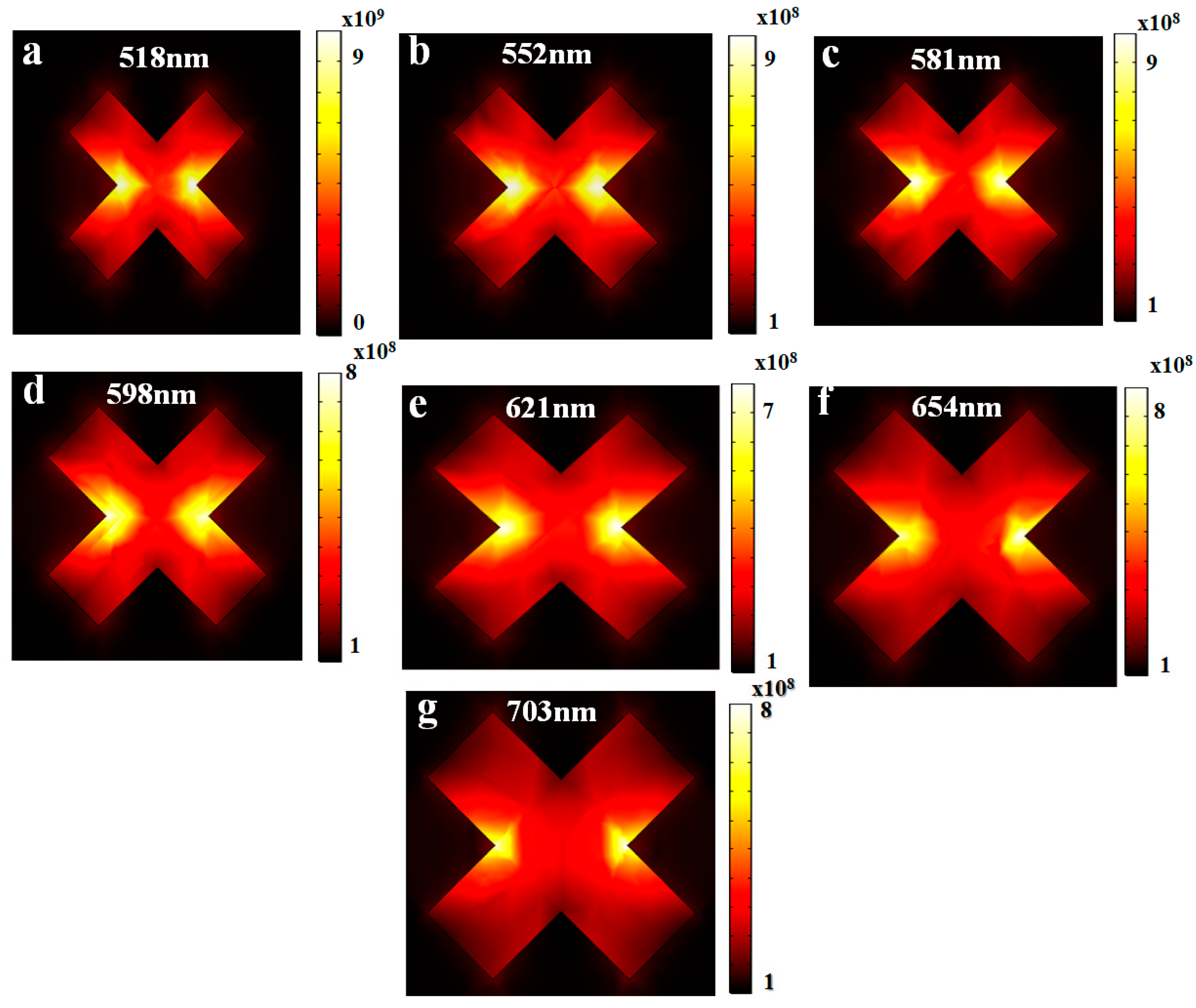
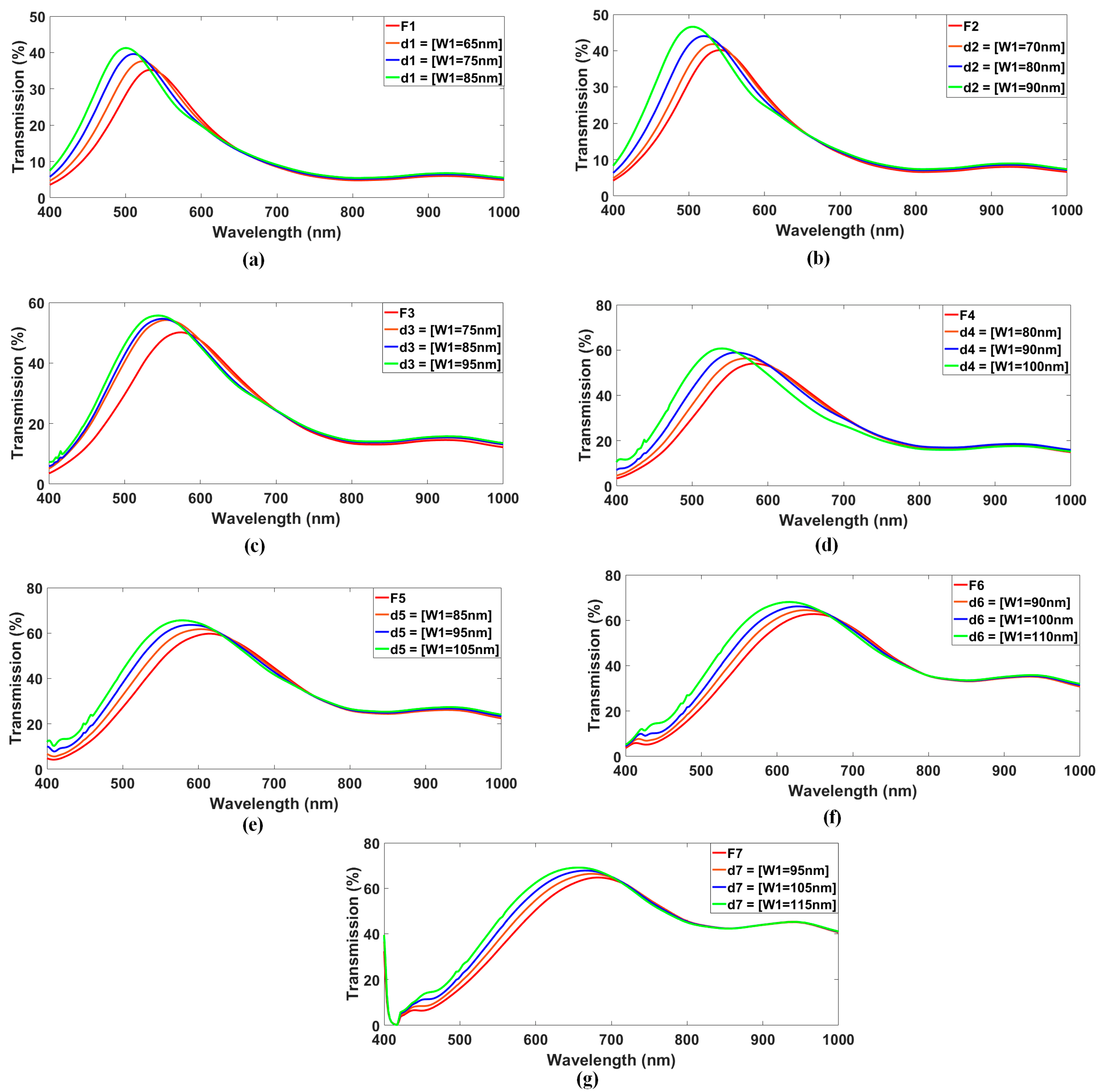
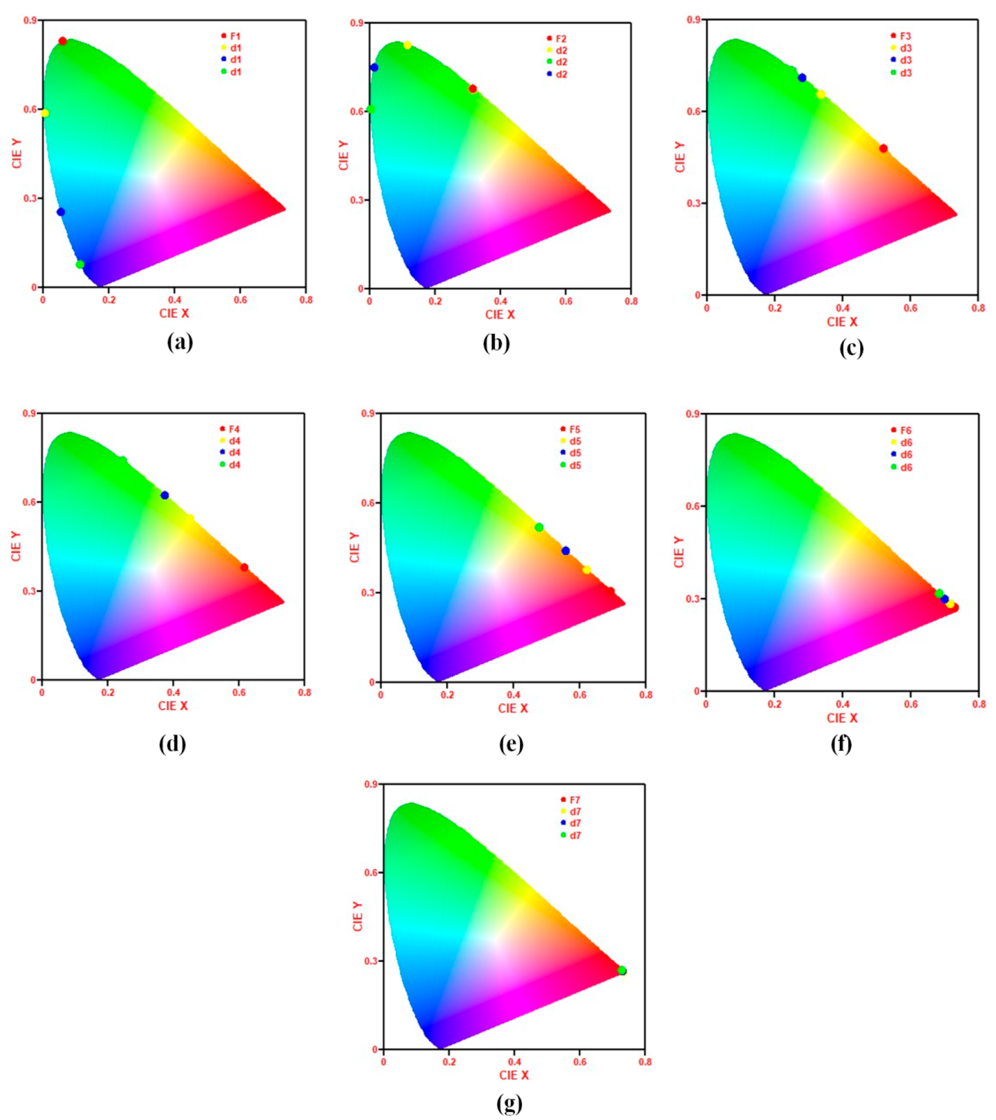
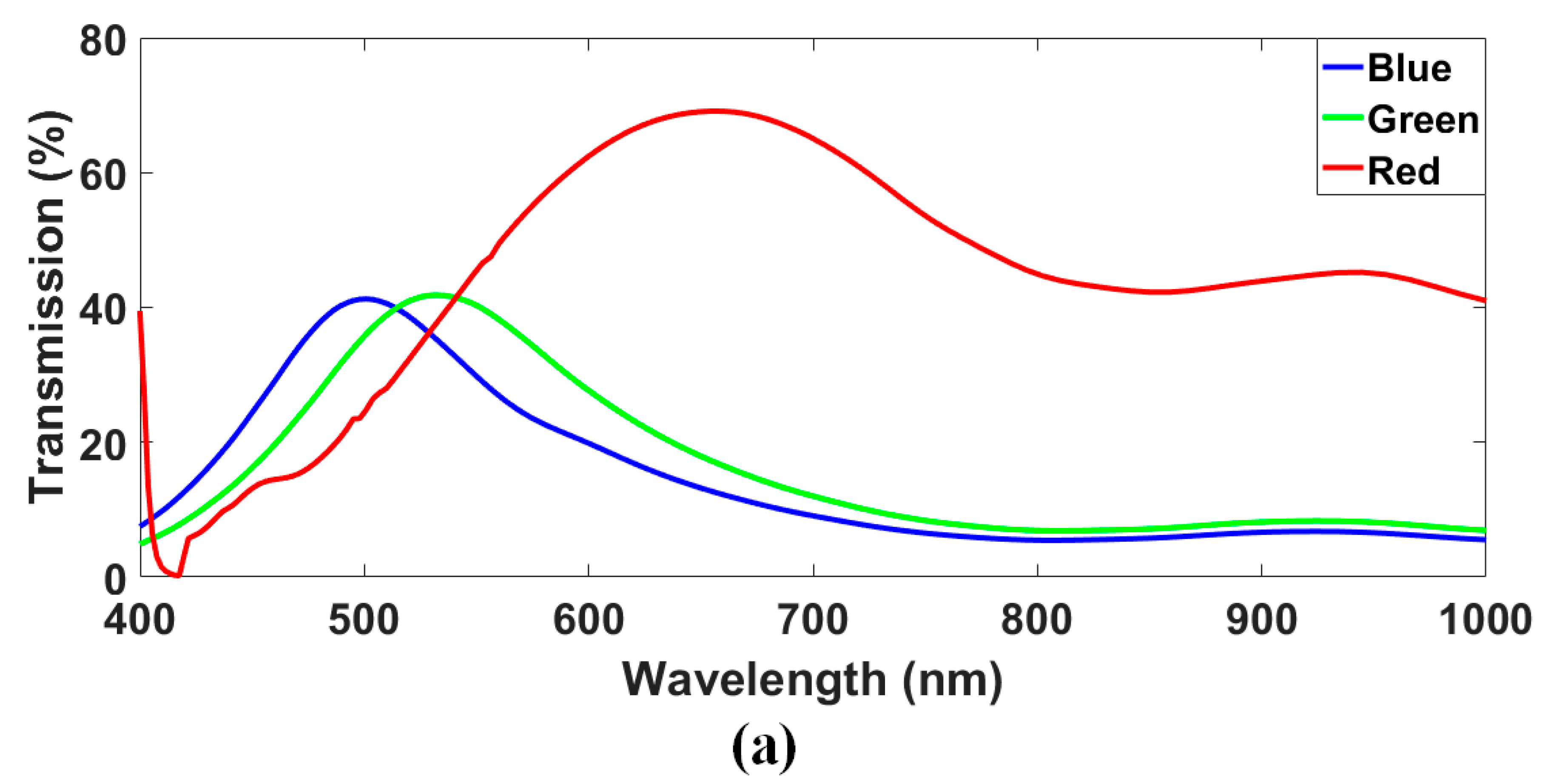
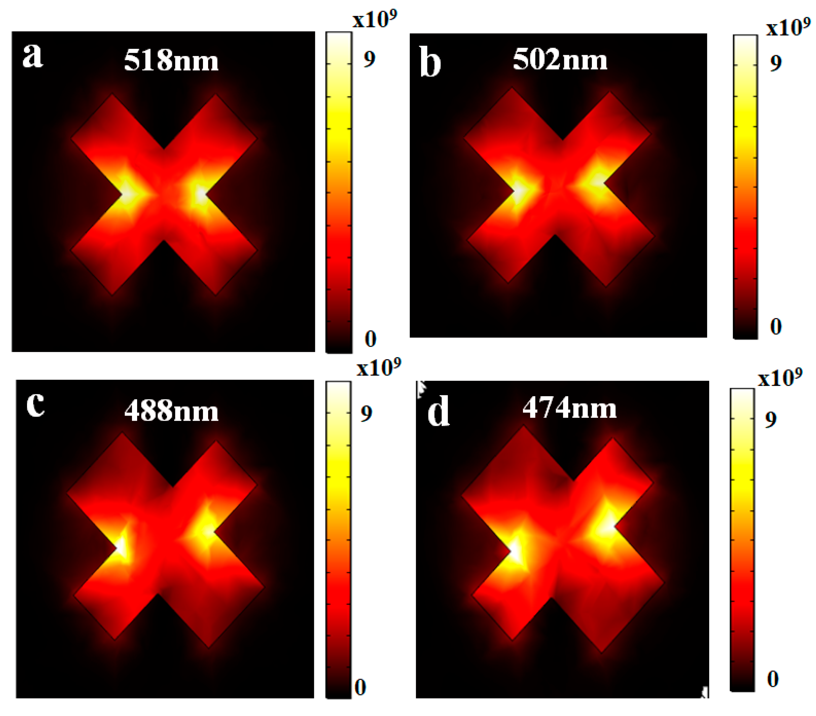
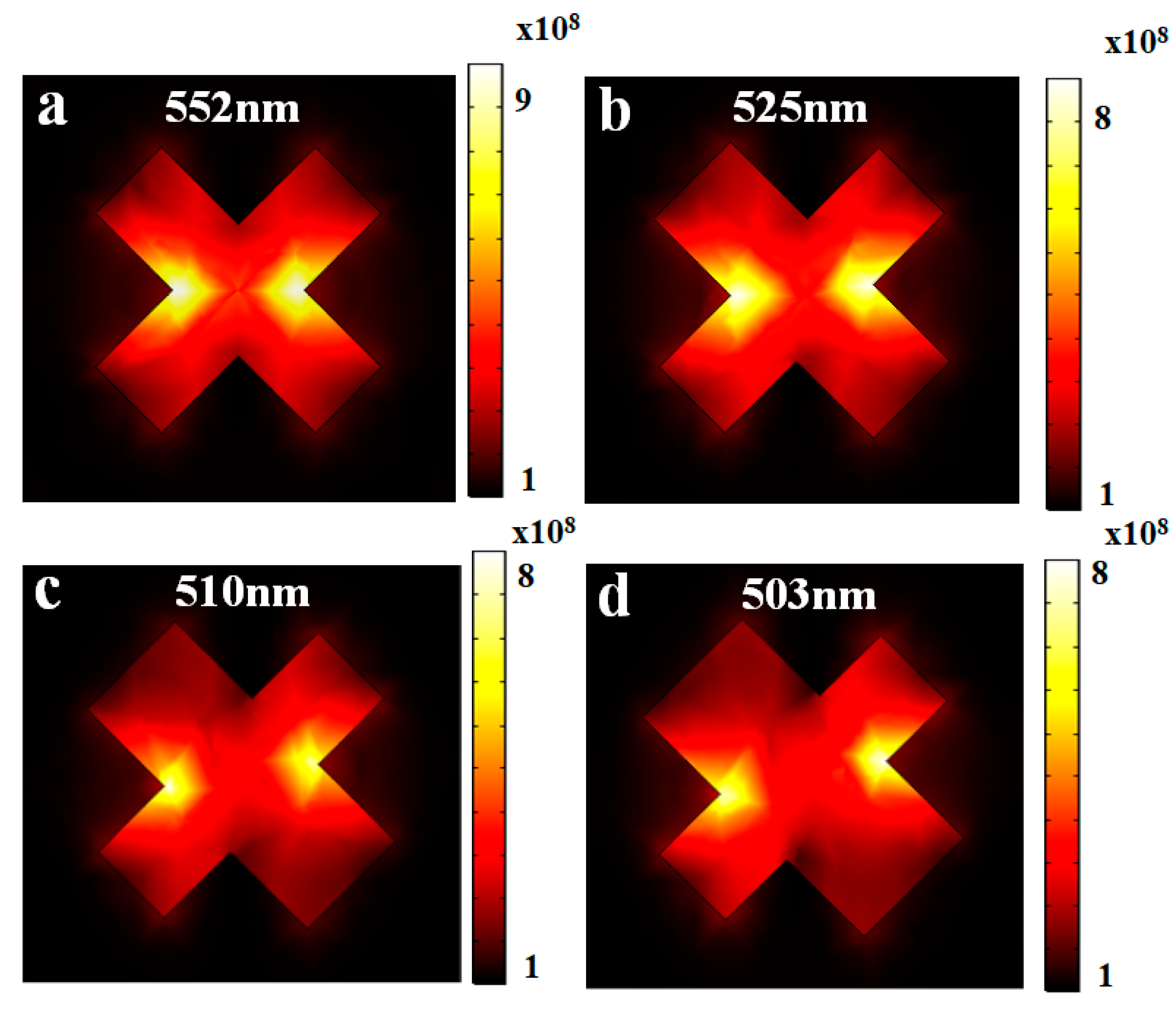
| Seven Extraordinary Optical Transmission Plasmonic Color Filter | Wavelength Shifts in Defects (d1–d7) | Transmission |
|---|---|---|
| F1 = 518 nm, T = 34% | d1 = 502 nm d1 = 488 nm d1 = 474 nm | 36% 38% 40% |
| F2 = 552 nm, T = 38% | d2 = 525 nm d2 = 519 nm d2 = 503 nm | 41% 44% 46% |
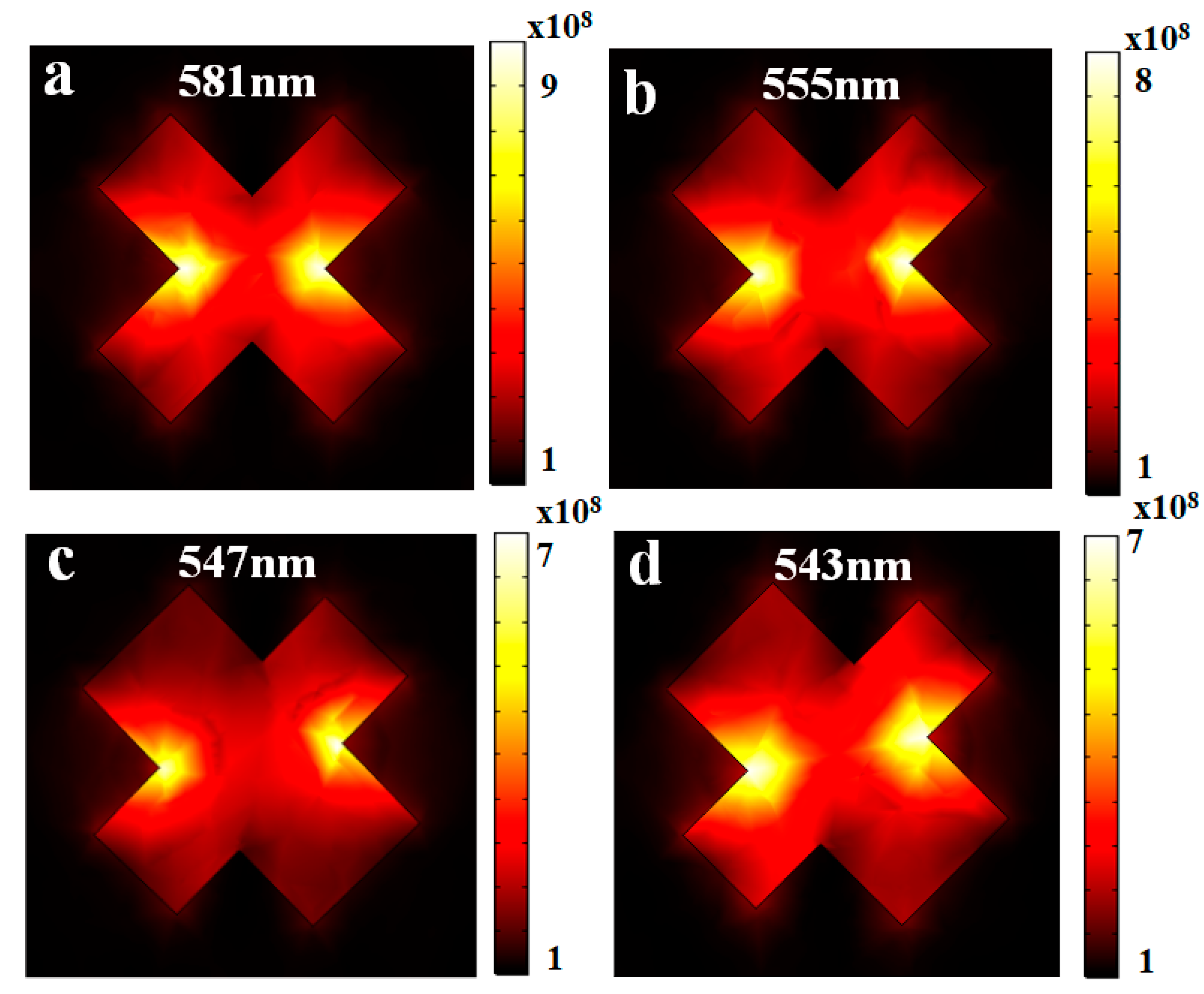
| F3 = 581 nm, T = 44% | d3 = 555 nm d3 = 547 nm d3 = 543 nm | 48% 50% 52% |
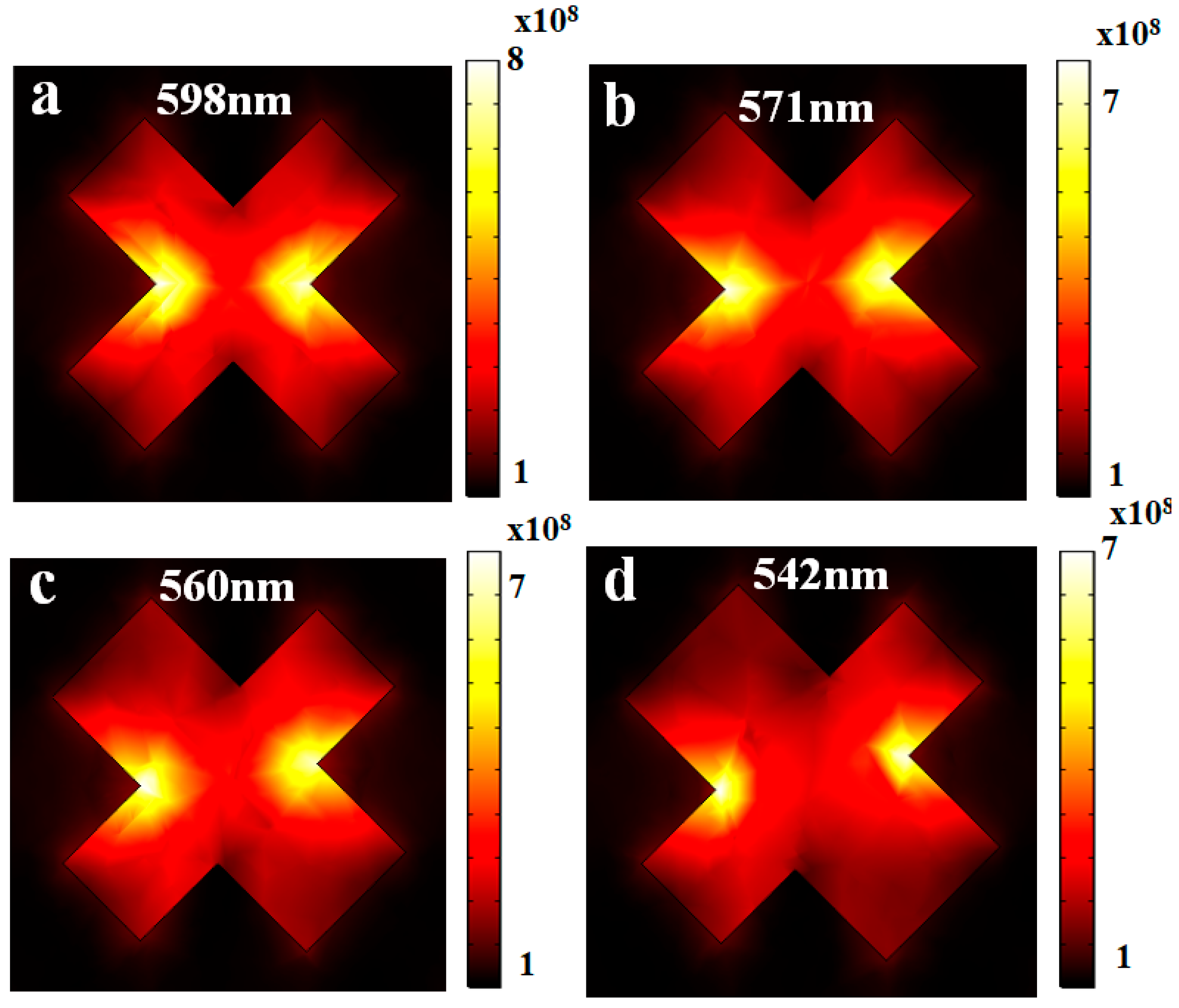
| F4 = 598 nm, T = 50% | d4 = 571 nm d4 = 560 nm d4 = 542 nm | 55% 58% 60% |
| F5 = 621 nm, T = 56% | d5 = 599 nm d5 = 587 nm d5 = 575 nm | 61% 63% 65% |
| F6 = 654 nm, T = 62% | d6 = 635 nm d6 = 625 nm d6 = 616 nm | 64% 66% 68% |
| F7 = 703 nm, T = 66% | d7 = 686 nm d7 = 670 nm d7 = 657 nm | 66% 67% 69% |
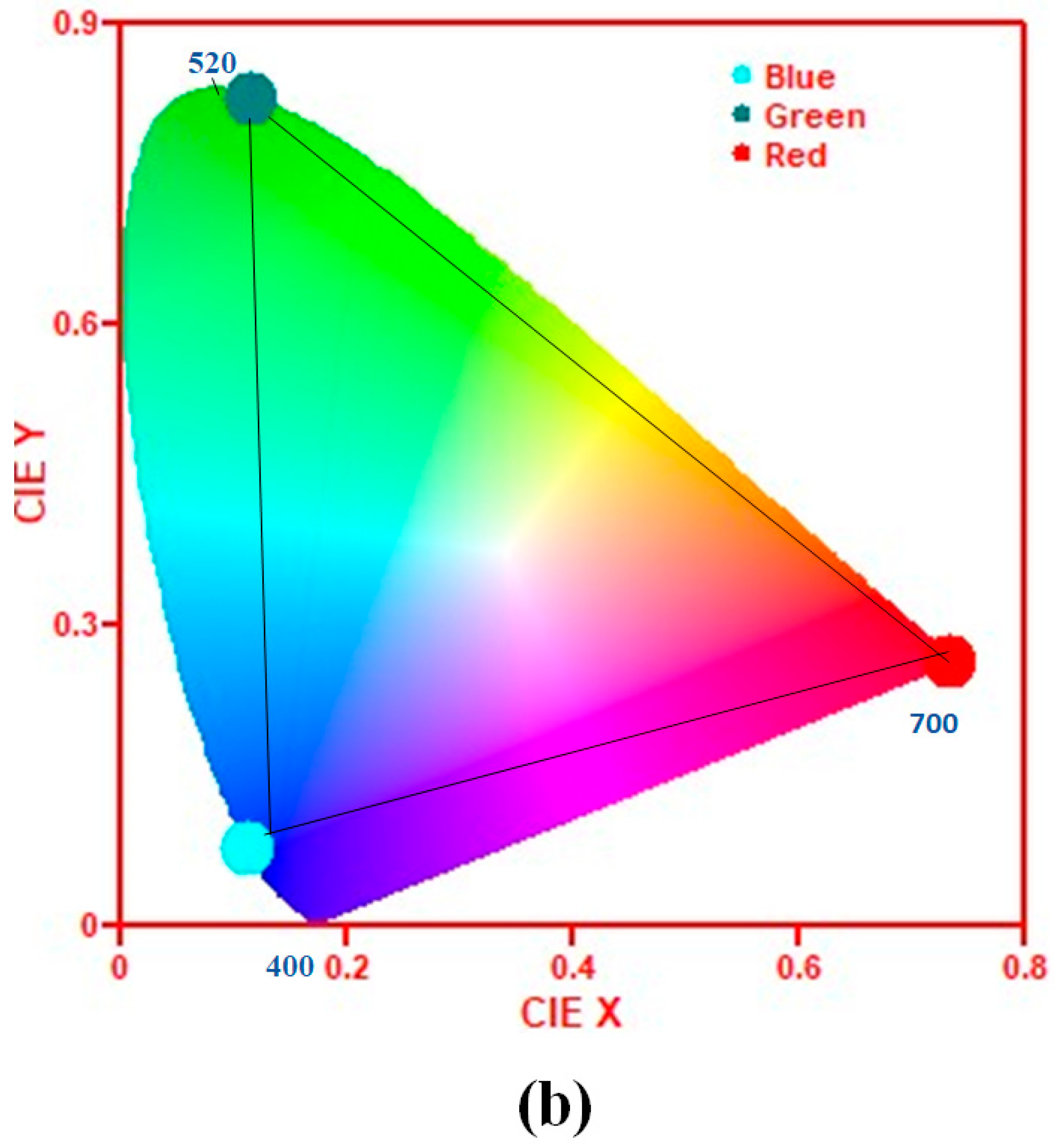
| References | Structure Type | Material | Color Gamut |
|---|---|---|---|
| [32] | Square array | Aluminum | sRGB |
| [33] | Circular array | Multilayer zinc sulphide and silver | sRGB |
| [34] | Square array | Silicon nitride | sRGB |
| [35] | Circular array | Aluminum and indium tin oxide | sRGB |
| [36] | Cross shaped with four rectangular edges | Silver and silicon dioxide | sRGB |
| [37] | Bowtie structure | Silver and silicon dioxide | sRGB |
| This study | X-shaped nanostructure | Aluminum and titanium dioxide | RGB |
Publisher’s Note: MDPI stays neutral with regard to jurisdictional claims in published maps and institutional affiliations. |
© 2022 by the authors. Licensee MDPI, Basel, Switzerland. This article is an open access article distributed under the terms and conditions of the Creative Commons Attribution (CC BY) license (https://creativecommons.org/licenses/by/4.0/).
Share and Cite
Shafiq, R.; Khan, A.D.; Al-Harbi, F.F.; Ali, F.; Armghan, A.; Asif, M.; Rehman, A.U.; Ali, E.M.; Arpanaei, F.; Alibakhshikenari, M.; et al. Optical Transmission Plasmonic Color Filter with Wider Color Gamut Based on X-Shaped Nanostructure. Photonics 2022, 9, 209. https://doi.org/10.3390/photonics9040209
Shafiq R, Khan AD, Al-Harbi FF, Ali F, Armghan A, Asif M, Rehman AU, Ali EM, Arpanaei F, Alibakhshikenari M, et al. Optical Transmission Plasmonic Color Filter with Wider Color Gamut Based on X-Shaped Nanostructure. Photonics. 2022; 9(4):209. https://doi.org/10.3390/photonics9040209
Chicago/Turabian StyleShafiq, Rehan, Adnan Daud Khan, Fatemah F. Al-Harbi, Farman Ali, Ammar Armghan, Muhammad Asif, Anees Ur Rehman, Esraa Mousa Ali, Farhad Arpanaei, Mohammad Alibakhshikenari, and et al. 2022. "Optical Transmission Plasmonic Color Filter with Wider Color Gamut Based on X-Shaped Nanostructure" Photonics 9, no. 4: 209. https://doi.org/10.3390/photonics9040209
APA StyleShafiq, R., Khan, A. D., Al-Harbi, F. F., Ali, F., Armghan, A., Asif, M., Rehman, A. U., Ali, E. M., Arpanaei, F., Alibakhshikenari, M., & Dalarsson, M. (2022). Optical Transmission Plasmonic Color Filter with Wider Color Gamut Based on X-Shaped Nanostructure. Photonics, 9(4), 209. https://doi.org/10.3390/photonics9040209