Abstract
Surface plasmon resonance sensors (SPR) using copper for sensitive parts are a competitive alternative to gold and silver. Copper oxide is a semiconductor and has a non-toxic nature. The unavoidable presence of copper oxide may be of interest as it is non-toxic, but it modifies the condition of resonance and the performance of the sensor. Therefore, the characterization of the optical properties of copper and copper oxide thin films is of interest. We propose a method to recover both the thicknesses and optical properties of copper and copper oxide from absorbance curves over the eV range, and we use these results to numerically investigate the surface plasmon resonance of copper/copper oxide thin films. Samples of initial copper thicknesses 10, 30 and 50 nm, after nine successive oxidations, are systematically studied to simulate the signal of a Surface Plasmon Resonance setup. The results obtained from the resolution of the inverse problem of absorbance are used to discuss the performance of a copper-oxide sensor and, therefore, to evaluate the optimal thicknesses.
1. Introduction
Surface plasmon resonance sensors are widely used for their high-sensitivity in real-time detection. Many improvements of the basic SPR [1], using a single gold layer as the active part of the sensor, have been proposed to improve the sensor performance [2]. For example, adding a specific absentee layer of KCL or Si3N4 or an absentee porous silica film can improve the performance of the SPR sensor by 5%, 11% and more than 300% [3,4]. The performance of the SPR sensor can be evaluated by the depth of the resonance dip, the full width at half maximum (FWHM) of the dip, the sensitivity to changes of the refractive index of the medium of detection and the figure of merit (FOM). The figure of merit is the ratio of the sensitivity to the FWHM. Indeed, a smaller FWHM gives a higher signal-to-noise ratio and higher measurement accuracy [3].
Copper presents interesting properties for optics, nanotechnology [5,6,7] and, therefore, for SPR sensors [8,9,10]. A recent paper demonstrated that the performance of a Cu-SPR sensor is quite similar to Au-SPR ones [9]. Moreover, bovine serum albumin (BSA) and other proteins do not bind irreversibly onto thin Cu-films. Copper phthalocyanine Langmuir–Blodgett films have been characterized using surface plasmon resonance (SPR) [11]. Exposure to toluene resulted in a partially reversible shift in the resonance depth and position of the SPR curves [12]. Moreover, the high cost of silver and gold materials—widely used in nanotechnologies—makes copper an adequate alternative to them.
Copper layers are naturally oxidized and their oxidation can be controlled by annealing. Copper oxides have non-toxic nature. The performance of SPR sensors depends not only on the metal layer used but also on dielectric layers above. Therefore, the study of Cu-oxide-SPR sensor performance requires finding out the thickness and optical properties of both materials, optical properties of copper and copper oxide thin films being different from those of bulk materials [13]. Consequently, to investigate Cu-oxide-SPR sensors, we first determine simultaneously the thicknesses and optical properties of 30 bilayers, from the fitting of absorbance curves. We detail the characteristics of the samples (Appendix A and Appendix B), the methods used for fitting (Appendix C), and the results (Appendix C.4) in the Appendix. Then, we use the recovered data to analyze numerically and discuss the Cu-oxide-SPR sensor performance. We propose the same electromagnetic approach to simulate the SPR signal and the metric of SPR performance (Section 2.2). The calculated SPR signals and performances are given in Section 3 and discussed in Section 4. Two cases are considered: the dry case (the upper medium is air), in which the SPR is used to analyze molecules in air, and the wet case (the medium of detection is water), in which the SPR characterize analytes in solutions. The optimal thicknesses are deduced from the performance parameters.
2. Materials and Methods
First, we summarize the method used to simultaneously determine the thicknesses and optical properties from experimental absorbance curves. This is an opportunity to detail the electromagnetic model of the generalized Fresnel coefficients also used for modeling the SPR sensor. We also give insights into the performance of SPR sensors.
2.1. Determination of Thicknesses and Optical Properties
The investigated samples are thin copper layers of target deposition thicknesses 10, 30 and 50 nm. They are successively annealed to control their oxidation under specific temperatures and for a given time. Thirty samples are characterized through the measurement of absorbance. Appendix A provides details on the sample preparation and experimental characterization [14]. The methods we propose for absorbance fitting and results are detailed in Appendix C.1, Appendix C.2, Appendix C.3 and Appendix C.4 and summarized in the following.
In Reference [15], we targeted the best fitting of UV-visible-NIR absorbance curves by a multilayer electromagnetic model using a function describing the optical properties over the range of investigated photon energies ( eV, i.e., nm). Our methodology relied on using a single metaheuristic optimization method and the Drude–Lorentz model for the optical properties of copper. Consequently, the inverse problem was solved, revealing the best parameters of the electromagnetic and materials models. In this paper, we improve the method proposed in [15] to recover the thicknesses and optical properties of thin layers of copper/copper oxide from absorbance measurements as follows.
- In the model of optical properties, we replace the Drude–Lorentz two-terms model of dispersion by a sum of partial fraction functions for fitting copper and copper oxide properties as a function of the photon energy ( and , respectively). is the order of the partial fractions model, also called the complex-conjugate pole-residue pair model [16]. is actually the number of poles in the function (see Equation (5)).
- We replace the two-steps method using first the bulk properties by a single multi-objective method, involving the error of fit and the relative difference between the optical properties we found and the bulk material properties. The purpose is to decrease the computational time.
- To achieve the fitting, we use three metaheuristic methods: Particle Swarm Method (PSO), Genetic Algorithm (GA), and Artificial Bee Colony method (ABC), with Gradient (GR) or Nelder–Mead simplex (NM) hybridization. Actually, metaheuristics are more or less efficient for achieving optimization, depending on the dimension of the problem (the number of input parameters of the model that have to be found) and on the topology of the objective function: the error of fit. Moreover, many realizations of the metaheuristics must be analyzed carefully to numerically characterize the stability of the solution and, hopefully, its uniqueness.
The calculation of the absorbance A is based on the electromagnetic model of the normal transmission of light across two plane material layers (with refractive index and thicknesses denoted and for copper, , for oxide). The copper layer is deposited on a dielectric glass substrate of refractive index (medium 1). The absorbance A is deduced from the transmitted intensity across the successive material layers according to:
where:
and
is the pure imaginary number, and is the magnitude of the illumination wave vector. The denominator is:
This electromagnetic model of generalized Fresnel coefficients includes the transmission of light across the Air-Quartz substrate . The optical properties of the glass substrate are measured before its coating with copper. The optical properties of copper and copper oxide are modeled as follows.
We use the partial fraction model, also called the complex-conjugate pole-residue pair model [16], to describe the dispersion of materials [17,18]. In a recent paper, the partial fraction model of dispersion yielded more accurate results than a sum of Drude–Lorentz functions to fit the bulk copper [18]. The relative permittivity is a complex number that is the square of the refractive index n:
where denotes the complex conjugate of Xy, is the model order (number of poles), is angular frequency of the incoming light (the photon energy is ). is the value of the limit of the permittivity when tends toward infinity and is actually the contribution of interband transitions. Therefore, it is spectrally located beyond the investigated energy range. are poles and are residues. The occurrence of poles in permittivity corresponds to light–matter damped resonances in the complex plane [19,20]. They can also be related to electronic transitions in materials. This partial fraction model is used for both copper and copper oxide. In this study, we use model order for copper oxide (semiconductor) and for copper (metal) to maintain sufficient accuracy on the optical properties.
Therefore, the number of unknowns of the problem is by splitting complex numbers into two real numbers: two thicknesses and parameters for each PF dispersion model ( for copper and for copper oxide). The model of absorbance (Equation (1)), including the models of optical properties (Equation (5)), is used within an evolutionary loop to find the best set of parameters for the model of absorbance. For the fitting of experimental UV-visible-NIR absorbance curves, a multi-objective function should be minimized to find the best input parameters of the fitting model.
The recovered parameters of the partial fraction model of dispersion (Equation (5)) are used to calculate the optical properties of copper and oxide at the wavelength of the laser incident light source ( nm) used by the SPR sensor.
2.2. The SPR Model
The SPR setup configuration (Figure 1) was modeled by the electromagnetic interaction of light with a plane multilayer [21,22]. The same approach has been used to study the influence of the functionalization layer [21] and adhesion layer for nanostructured Au-EPR [23,24]. The light source is considered as a monochromatic plane wave of wavelength nm (photon energy eV). For simplicity, we choose the same refractive index for the SPR prism as that used for the glass supporting the copper/copper oxide sample.
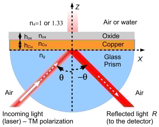
Figure 1.
Schematic of the prism-based SPR sensor with the Kretschmann configuration. The plane material layers are deposited on the hemispherical lens.
The SPR detected signal R is a function of the incident angle of the plane wave from normal to the multilayer surface:
where and are the transmitted intensities of the light incoming and outcoming from the SPR setup (see Equation (2)). The reflected amplitude is :
being the normal to the surface of multilayer component of the wave vector. In medium m, this component is , with , c being the speed of light in vacuum. The refractive index of the detection medium of the SPR sensor is . The denominator of the transmitted amplitude is:
We obtain (Equation (4)) by considering normal incidence of the light () and . However, Equation (4) is used for the fitting of experimental UV-visible-NIR absorbance, as it requires less computational time.
The basics of SPR are given in Reference [25]. In that reference, we gave the conditions of SPR excitation on an interface between two mediums and the corresponding formula, also used in [9]. Considering a plane interface between two media (one of them is a metal), the SPR angle can be easily evaluated, and being the relative permittivities of materials on both sides of the interface, and being that of the hemispherical glass substrate, and ℜ the real part:
We consider the angle interrogation mode of the SPR sensor [2,9,12]. At a given wavelength, in the Angular Interrogation Mode (AIM), with a changing refractive index of water (upper medium, analyte), the resonance angle shifts [4].
2.3. Performance of the SPR Sensor
The performance parameters of the SPR sensor are the sensitivity , the full width at half maximum () and the Figure of Merit () [4]. The resonance angle found at the minimum of reflectance (), and the depth of the resonance dip () are also of interest to characterize SPR sensors. The performance of SPR can help to determine the optimal thicknesses of the bilayer.
2.3.1. Sensitivity
The sensitivity of the SPR sensor is the angular shift that is found at the minimum of reflectance by varying the refractive index of the medium of detection. The angular sensitivity is, therefore:
where is the relative index of refraction unit: . The greater the sensitivity is, the better performance of SPR.
2.3.2. Full Width at Half Maximum
The full width at half maximum is:
The thinner the resonance dip is, the higher is the signal to noise ratio of the SPR sensor [3].
2.3.3. Figure of Merit
Therefore, the figure of merit of the SPR sensor is deduced from both the sensitivity and the full width at half maximum of the reflectance (FWHM) [4]:
The thinner the wells in the reflectance (small value of FWHM), the more enhanced the FOM. The greater the sensitivity deduced from the shift of the minimum in reflectance by a change of optical index of the upper medium, the greater the FOM. However, the FOM does not take into account the value of the minimum in reflectance . This minimum should be as close as possible to zero to obtain high dynamic of detection.
2.4. Optimal Thicknesses
Interference conditions in the metal layer have been considered in Reference [26] to find the optimal thickness of a classical SPR sensor. This condition relies on the calculation of the copper thickness that verifies constructive interference at the copper–oxide interface, after two reflections on the interfaces [27]:
with m an integer number and and the Fresnel coefficients of reflection on each interface. The real part of is actually an approximation of the optimal thickness, by neglecting the finite thickness of oxide. However, this criterion can be extended by calculating the argument of the sum of the illumination field and of the reflected one (Equation (7)) that should be as close as possible to 0. In this case, we obtain a minimum of reflectance (destructive interference between the illumination and the reflected wave). This minimum corresponds to a pole (complex number) of the generalized Fresnel coefficient (Equation (7)) [19,28].
2.5. Investigated Samples
The manufacturing and characterization of the investigated samples are detailed in Appendix A and Appendix B. The fitting methods are described in Appendix C, and the full results are given in Appendix C.4 (thicknesses of the copper and oxide layers, optical properties nm, eV) for each of the thirty investigated samples. We summarize the main results shown in Table A3, Table A4 and Table A5:
- Copper and copper oxide thicknesses are globally in agreement with those obtained from experimental measurements (see Appendix B).
- The real part of the relative permittivity of copper is smaller than the bulk one for almost all samples. The imaginary part of the relative permittivity of copper is about twice the bulk one. The mean value of over the samples with nm is (standard deviation ) compared to [29].
- The real part and the imaginary parts of the relative permittivity of oxide are close to that of the bulk, except for full oxidized samples for which both parts decrease. This behavior is probably due to air inclusion in oxide (the grain size of oxide can reach 80 nm, see Appendix B). The mean value of over the samples with nm is (standard deviation ) compared to and [29]. If we suppose a chemical mix of both oxides, we deduce that oxide may be made of 76% Cu2O and 24% CuO. This result was confirmed by XPS measurements [14,30]. The decrease in the real part of the oxide permittivity may also be due to air inclusion in oxide.
- For samples with roughness varying from 2 to 14 nm [14], the electromagnetic model of generalized Fresnel coefficients could be accurate enough. The quality of absorbance fitting shown in Figure A1, Figure A2, Figure A3, Figure A4, Figure A5, Figure A6, Figure A7, Figure A8, Figure A9, Figure A10 and Figure A11 confirms the validity of the model, which can therefore be used to model the SPR.
3. Results
In this section, we use the thicknesses and optical properties that are simultaneously recovered from the fitting of absorbance curves (Table A3, Table A4 and Table A5) to study the SPR sensor setup, of which the sensitive part is a copper and copper oxide bilayer. From these results, we calculate the signal of the SPR sensor working in angular interrogation mode for air and water as the upper medium: in the dry and wet cases, respectively. We also evaluate the performance of such set up. We use .
3.1. Dry Case
Figure 1 illustrates the SPR setup. The wavelength of laser illumination is nm. The photon energy of the excitation light ( eV) is close to that of the transition from d states (valence band) to th es-p conduction band [18] (2.1 eV, see the vertical black line in Figure A1, Figure A6 and Figure A11). Therefore, we expect a good quality of the plasmon resonance for adequate thickness of copper: a sharp dip and a small minimum.
Figure 2, Figure 3 and Figure 4 show the simulation of the SPR setup signal from the model of reflectance in Equation (6), considering air as the upper medium. The reflectance curves are plotted as functions of the incident angle of illumination (at nm) for each investigated sample.
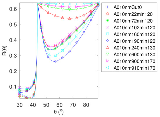
Figure 2.
Simulated SPR setup signal for the samples of initial target thickness 10 nm. The calculation uses the parameters deduced from the fitting of UV-visible-NIR absorbance curves. The optical properties of copper and copper oxide are calculated at wavelength nm. Upper medium is air.
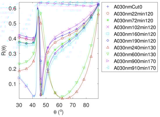
Figure 3.
Simulated SPR setup signal for the samples of initial target thickness 30 nm. The calculation uses the parameters deduced from the fitting of UV-visible-NIR absorbance curves, at wavelength nm. Upper medium is air.
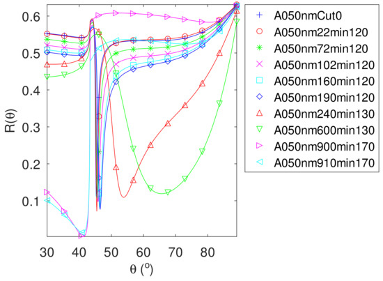
Figure 4.
Simulated SPR setup signal for the samples of initial target thickness nm. The calculation uses the parameters deduced from the fitting of UV-visible-NIR absorbance curves, at wavelength nm. Upper medium is air.
In Figure 2, for negligible thicknesses of copper (less than 2 nm), the reflectance is characteristic of a dielectric material. In the other cases, the wells in reflectance on the right correspond to the absorption of photon energy by the copper layer (resonance). Nevertheless, the quality of the surface plasmon resonance is low: the wells are wide and the depths of dip are greater than 0.26.
The surface plasmon dip for copper thicknesses close to 30 nm are thinner than in the previous case (Figure 3 vs. Figure 2). The smallest values of R (depth of dip) are close to each other for nm near 30 nm. The SPR angles are close to . This SPR angle is close to that of a copper–air interface. The influence of the thin layer of oxide on the SPR angle is negligible for oxide thicknesses below 3.5 nm. However, the shape of the curve seems to be clearly modified, even for small thicknesses of the oxide. Thus, we can anticipate that the thickness of oxide will have an influence on the FWMH. For thicker oxide layers, the dip is widened and the SPR resonance angle approaches , which is not so far from that of the copper–oxide interface ().
The SPR dips are thinner for the six samples for which nm and are smaller than that for the previous samples (Figure 4 compared to Figure 2 and Figure 3). By decreasing , the SPR dips are enlarged and shifted, as in the previous case. The performance parameters introduced above can be evaluated for the investigated samples.
The best performances of the SPR using the investigated bilayers as sensitive parts are shown in Table 1 [3,4]. We indicate both the retrieved thicknesses of copper and oxide (, ) from absorbance curves, and the corresponding optical properties (, ) nm (extracted from Table A5). We give the resonance angle , the depth of dip , the full width at half maximum of the SPR dip (FWHM, Equation (11)), the sensitivity (Equation (10)), and the figure of merit (FOM, Equation (12)). The uncertainty on FOM is indicated in between brackets. This is the standard deviation of FOR for the recovered parameters of the multi-objective function (see Appendix C). We also give the FOM calculated with the bulk optical properties for Cu and Cu2O [29] and without the oxide layer for comparison.

Table 1.
Calculated performance of the SPR setup given the retrieved thicknesses and optical properties in the dry case: resonance angle, the depth of SPR dip, full width at half maximum, sensitivity and figure of merit (only FOM RIU are indicated) and its uncertainty, FOM for optical properties of bulk materials, and for bare copper (without oxide).
The resonance angle is close to that of the interface between copper and the medium of detection (Equation (9), ). The minimum of reflectance is smaller than and the sensitivity is about the same for all samples. The FWHM is smaller for copper thicknesses close to 50 nm; therefore, the value of FOM is greater. The uncertainty on FOM is small for almost all cases. The thickness of oxide being negligible, the FOM for copper without oxide is about the same. The values of are greater than 62.7. On the contrary, the FOM calculated from bulk optical properties of copper and copper oxide are different. This is due to the value of the real part of the copper relative permittivity, which is smaller than that of bulk copper (). This confirms the interest in simultaneously measuring the optical properties of copper and oxide for thin films.
In the general case, for a given thickness of copper and increasing thickness of oxide, the angle of resonance is shifted to the right, the FWHM increases as well as the depth of the SPR dip, and the FOM decreases.
The results for the investigated samples show that plasmon resonance can be launched for specific thicknesses. Therefore, the performance of the copper/copper oxide SPR setup deserves to be specifically studied, assuming that the medium of detection is water (wet case).
3.2. Wet Case
Table 2 restates the best thicknesses of copper and oxide, the retrieved relative permittivity ( and ) extracted from Table A4 and Table A5 and the calculated performance of SPR for samples with FOM > 20.
Table 2.
Calculated performance of the SPR setup given the retrieved thicknesses and optical properties in the wet case: resonance angle, the depth of SPR dip, full width at half maximum, sensitivity and figure of merit (only FOM RIU are indicated) and its uncertainty, FOM for optical properties of bulk materials, and for bare copper (without oxide).
The prism-SPR performance is evaluated as in the dry case. For water as upper medium, the SPR angle is greater than for air. The SPR angle falls between the SPR of the copper–oxide interface (72.4) and that of the glass–copper interface (86.7). On the contrary of the dry case, the samples with copper thicknesses around 28 and 30 nm give a reflectance smaller than 0.11 and FOM greater than 20. In this case, the values of both the sensitivity and the figure of merit are about the same whatever the oxide thickness is. The maximum of FOM is reached for thicker copper layers (near 50 nm), as in the dry case. The figure of merit is also calculated from the best values but by neglecting the oxide layer. In this case, we suppose that the bare copper layer is directly in contact with the above medium. Let us emphasize that the presence of oxide decreases the FOM (see FOM and FOM ox. free). This result is in agreement with that obtained for gold-SPR coated with porous silica film [4]. The performance of SPR working in dry and wet cases depends strongly on the thickness of both layers. The maximum sensitivity is obtained for the optimal thicknesses of 28 and 3 nm for copper and oxide, respectively, and for 49.8 and 0.6 nm.
4. Discussion
4.1. Cu-Oxide-SPR Performance
The performance of Cu-oxide-SPR in dry and wet cases are of the same order of magnitude as that mentioned in Reference [4] for silver/porous silica (wet case). The slight decrease in FOM by using a dielectric coating of metal can also be observed for our samples, for which the thickness of oxide is lower than 3.5 nm. The best values of FOM are obtained for oxide thicknesses lower than 3 nm. We observe that the FOM is highly sensitive to changes in the refractive index of copper. The FOM value is slightly greater than that obtained with Au, Au/Si3N4, Au/KCl materials [3]. The values of sensitivity and FWHM are greater in the wet case than in the dry case, leading to a smaller figure of merit.
In addition to its non-toxic nature, the oxide layer can be used to tune the position of the SPR resonance [9]. Indeed, the oxide layer could be used to adjust the resonance near the copper transition 2.1 eV that is characteristic of the inter-band transition from d states (valence band) to the ‘s-p’ conduction band [18] (Figure A1, Figure A6 and Figure A11 where the vertical line shows the photon energy of illumination used in the SPR setup eV). Let us note that cuprous copper oxide (Cu2O) and cupric copper oxide (CuO) are p-type semiconductors with a bandgap of approximately 2.2–2.9 and 1.2–2.1 eV, respectively.
The optimal copper thickness (around 50 nm) is coherent with that found in Reference [9] ( nm), even if the substrate (prism) and the wavelength were not the same. However, these results show that more than one copper thickness may be used to design an efficient SPR sensor. This is the consequence of the high dependence of the optical properties on both the thickness and the sample elaboration mode (temperature and annealing time).
The SPR angle is around 46 in the dry case and 80 in the wet case. This last value is close to those obtained with a Al2O3 coating [10], and with BK7 substrate [9], both in the wet case. These SPR angles can also be compared to the SPR angles of single interfaces (Equation (9)). In the dry case, the shift of SPR angle is about 1–2 for oxide thicknesses below 2 nm. In the wet case, the shift is greater and falls between that of the glass/copper and copper/water interfaces. Therefore, the coupling of both SPR differs for two different mediums of detection.
Therefore, the performance parameters may reveal different properties of the SPR-sensor. In the next section, we discuss the optimal thickness obtained from the best performance parameters.
4.2. Optimal Thicknesses
The thicknesses of copper for the investigated samples are not sufficient to determine the optimal thickness. Nevertheless, the small dispersion of retrieved optical properties of copper and oxide leads us to use their mean value to determine the optimal thicknesses of copper and oxide layers. Actually, the mean value is (standard deviation ) and (standard deviation ), see Section 2. They differ from the bulk values [29]. Therefore, we can use the mean values of the optical properties and a scan of copper thicknesses from 10 to 70 nm, and oxide thickness in (1;60) nm, in steps of 0.5 nm, to evaluate the optimal thicknesses from the best performance parameters and interference conditions, as explained in Section 2.4, in the dry and wet case. Table 3 and Table 4 give the mean value and the standard deviation of the top 1% results for each performance parameter.
Table 3.
Mean optimal thicknesses for the top 1% performance parameters of the SPR set up in the dry case according to the minimum of reflectance, sensitivity, full width at half maximum, figure of merit and argument of the total field on the glass-copper interface. In brackets, standard deviation of the top 1%.
Table 4.
Optimal thicknesses for the top 1% performance parameters of the SPR set up in the wet case according to the minimum of reflectance, sensitivity, full width at half maximum, figure of merit and argument of the total field on the glass–copper interface. In brackets, standard deviation of the top 1%.
The argument of should be close to 0 for these optimal values. This means that the conditions of destructive interference between incident and reflected waves are almost fulfilled and the minimum of reflectance is reached. The optimal thickness can be found for the maximum of FOM (Equation (12)) or sensitivity (Equation (10)), or for the minimum of FWHM and reflectance .
In the dry case, the best thicknesses of copper are close together for and , on the one hand, and for , and on the other hand. If the conditions of constructive interference in the copper layer are fulfilled (Equation (13)), the optimal thicknesses of copper found are 29 nm for , 48 nm for . Therefore, we can deduce that all the copper thicknesses in Table 3 correspond to optimal ones, but for different optimal parameters. Moreover, these values are in agreement with that obtained from investigated samples in Section 3. The optimal thickness of copper for is between those for and . Therefore, the optimal thicknesses can be deduced from a selection of the solution with the minimum of among the top 1% solutions for : nm, nm, , , .
In the wet case, the best thicknesses of copper are close together for and , on the one hand, and for and on the other hand. If the conditions of constructive interference in the copper layer are fulfilled (Equation (13)), the optimal thicknesses of copper found are 29 nm for , 42 nm for . Again, we can deduce that all the copper thicknesses in Table 3 correspond to optimal ones, but for different optimal parameters. Furthermore, these results are also in agreement with that obtained from investigated samples in Section 3. The optimal thickness of copper for is close to that for the performance parameter. As in the dry case, the optimal thicknesses can be deduced from selection of the solution with the minimum of among the top 1% solutions for : nm, nm, , , .
5. Conclusions
The performance of Cu-oxide-SPR has been studied, including the influence of copper oxide. To reach this goal, we have used the fitting of experimental UV-visible-NIR absorbance curves to simultaneously obtain the thicknesses and optical properties of copper/copper oxide samples. For this, more than one metaheuristic is of interest. We found that the optical properties of copper and copper oxide vary as a function of the thicknesses and differ from the bulk ones. The performance of Cu-oxide-SPR confirms that copper/copper oxide could be a valuable alternative to gold for SPR sensors. The performance parameters reveal different optimal thicknesses in the dry and wet cases. For a systematic study of the optimal thickness, the combination of the maximum of FOM and the minimum of reflectance could be an interesting alternative to find the optimal thickness. The relevance of the result depends on the accurate determination of thicknesses and optical properties of the bilayer. At nm, with , , the optimal thicknesses of copper and oxide layers are about 44 and 1 nm in the dry case, and 41 and 1 nm in the wet case. They are determined to maximize the FOM and to minimize the dip magnitude. To optimize the SPR setup, we suggest the following process.
- Production series of samples with controlled annealing under low temperature;
- Characterization of samples (measurement of thickness and optical properties) from absorbance curves, for example;
- Characterization of samples in angular interaction mode;
- Fit of the SPR signal to verify the optical properties;
- Selection of the best sample and verification at regular time intervals that the thicknesses and optical properties remain the same.
Actually, the method of fit proposed in this paper could be applied to an SPR signal. In the future, we also intend to apply (and adapt if necessary) our method to characterize SPR with a multilayer sensitive part.
Author Contributions
Conceptualization: D.B. and T.G.; methodology, D.B. and T.G.; software: D.B.; validation, T.G.; formal analysis: D.B. and T.G.; investigation, D.B. and T.G.; experimental resources: D.C., E.A. and N.F., data curation: D.C., E.A. and N.F.; writing—original draft preparation: D.B.; writing—review and editing: D.B., T.G., S.K., E.A. and N.F.; supervision: D.B.; project administration: D.B.; funding acquisition: D.B., R.M., E.A. All authors have read and agreed to the published version of the manuscript.
Funding
This research was funded by the European Regional Development Fund grant number CUMIN CA0021200.
Institutional Review Board Statement
The study was conducted according to the guidelines of the European Charter for Researchers. https://euraxess.ec.europa.eu/jobs/charter/european-charter.
Informed Consent Statement
No Human Subjects of Research.
Data Availability Statement
Data available on request.
Conflicts of Interest
The authors declare no conflict of interest. The funders had no role in the design of the study; in the collection, analyses, or interpretation of data; in the writing of the manuscript, or in the decision to publish the results.
Abbreviations
The following abbreviations are used in this manuscript:
| AIM | Angular Interrogation Mode |
| ABC | Artificial Bee Colony |
| EM | Evolutionary Method |
| FOM | Figure of Merit |
| FWHM | full width at half maximum |
| GR | method of gradient descent |
| NM | Nelder–Mead Simplex Method |
| PSO | Particle Swarm Optimization |
| SPR | Surface Plasmon Resonance |
Appendix A. The Samples Preparation
Deniz Cakir prepared and characterized the copper/copper oxide [14] at Laboratoire Charles Coulomb, UMR CNRS 5221, Université de Montpellier, under the supervision of Eric Anglaret and Nicole Fréty [15]. The copper nanolayers were deposited by thermal evaporation on fused silica substrates (optical grade from Neyco). Before deposition, the substrates were cleaned in an acetone bath with ultrasounds for 5 min, and then plasma-treated in a 70% O2/30% N2 atmosphere for 6 min. The copper wire of purity of 99,999%, bought from Alfa Aesar, was placed 18 cm below the target substrate. The sublimation of the Cu wire was achieved under 120 A, at 10-5 mbar, using a tungsten crucible as the counter-electrode. The target thicknesses (nominal thickness before oxidation) of the copper layers are = 10, 30, and 50 nm. Copper thin films were annealed under air at atmospheric pressure. Low annealing temperatures were chosen to preferentially obtain Cu2O [30,31,32,33,34,35,36]. Samples were annealed progressively for increasing times and temperatures following the thermal treatment, as detailed in Table A1. For each annealing condition and layer thickness, absorbance was measured with a UV-visible-NIR spectrometer (Cary 5000, Agilent, Les Ulys, France) over the spectral range 350–1380 nm, using a beam diameter of 1 mm. for each annealing condition. Therefore, 30 absorption spectra are available for fitting by the model described in this paper.
Table A1.
Sample preparation. Three samples of copper initial target thicknesses 10, 30 and 50 nm were successively annealed.
Table A1.
Sample preparation. Three samples of copper initial target thicknesses 10, 30 and 50 nm were successively annealed.
| Annealing Time (Min) | Temperature ( C) | Reference Name of Data |
|---|---|---|
| 0 | 20 | A0XYnmCut0 |
| 22 | 120 | A0XYnm22min120 |
| 72 | 120 | A0XYnm72min120 |
| 102 | 120 | A0XYnm102min120 |
| 160 | 120 | A0XYnm160min120 |
| 10 | 120 | A0XYnm190min120 |
| 240 | 130 | A0XYnm240min130 |
| 600 | 130 | A0XYnm600min130 |
| 900 | 170 | A0XYnm900lin170 |
| 910 | 170 | A0XYnm910min170 |
Appendix B. Measurement of Thicknesses
Cross-sections of the raw and fully oxidized samples were characterized using Scanning Electron Microscopy (SEM, Helios NanoLab 660 FEI and High resolution Hitachi S4800) and Atomic Force Microscopy (AFM, Dimension 3100 NanoScope IIIa, Bruker, Wissembourg, France). The AFM equipment was used in tapping mode using silicon nitride cantilevers with sharpened pyramidal tips. Multiple-Angle Incident (MAI) ellipsometry (Multiskop, Optrel GbR, Kleinmachnow, Germany), with green laser light = 532 nm and Spectroscopic Ellipsometry (SE, Nanofilm EP4, Accurion GmbH, Göttingen, Germany) were also used in addition to spectroscopic ellipsometry monochromatized light at 560, 660, 760, 860 and 960 nm. The results we obtain in this study are reported in Table A2 (UV-vis-NIR, NIR CARY 5000, Agilent, Les Ulys, France) extracted from Table A3, Table A4 and Table A5.
The transformation of a mole of metallic copper to oxide is leading to a volume increase that is evaluated to for Cu2O and for CuO:
where is the number of copper atoms in a molecule of oxide, , are the molar mass, and , are the densities. In Table A2, this metric is evaluated considering uniaxial growth with a fixed section:
Cuprous oxide is expected to be highly dominant at low-temperatures of annealing [30].
Table A2.
Measured thicknesses (nm) of raw and fully oxidized samples.
Table A2.
Measured thicknesses (nm) of raw and fully oxidized samples.
| Sample | SEM | AFM | MAI | SE | UV-Vis-NIR |
|---|---|---|---|---|---|
| A010nmCut0 | − | 11 ± 3 | 7.2 ± 0.1 | 11.0 ± 0.2 | 9.8 ± 0.2 |
| − | 0.2 ± 0.1 | 3.4 ± 0.2 | 1.8 ± 1.1 | ||
| A030nmCut0 | − | 31 ± 5 | 28.2 ± 0.1 | 38.7 ± 1.3 | 30.0 ± 0.1 |
| − | 2.9 ± 0.1 | 3.7 ± 0.2 | 0.0 ± 0.7 | ||
| A050nmCut0 | − | 51 ± 8 | − | − | 50.0 ± 0.1 |
| − | − | 5 ± 0.9 | 0.1 ± 0.2 | ||
| A010nm900min170 | 34 ± 7 | 26 ± 3 | 5.6 ± 0.1 | 0.9 ± 0.4 | 1.2 ± 0.5 |
| 19.6± 0.1 | 20.3 ± 3.1 | 19.7 ± 1.6 | |||
| A030nm900min170 | 104 ± 29 | 98 ± 23 | 4.9 ± 0.1 | 0.3 ± 1.4 | 0.6 ± 4.2 |
| 84.6 ± 0.1 | 63.1 ± 7.4 | 44.8 ± 6.6 | |||
| A050nm900min170 | 136 ± 15 | 142 ± 30 | − | 0 ± 7.9 | 0.0 ± 0.6 |
| − | 87.3 ± 3.7 | 89.6 ± 4.4 | |||
| − | − |
AFM and SEM measurements are the real thicknesses of samples, whereas MAI, SE spectroscopies and UV-vis-NIR give effective thicknesses. Copper films show a very fine microstructure, with a grain size of a few nm, and a very low roughness with a value of about 1 nm. The grain size of oxide and perhaps the slice process explain the values from AFM and SEM and the high magnitude of . This microstructure remains thin after full oxidation with a grain size varying from a few to 80 nm according to the oxide thickness and a roughness varying from 2 to 14 nm. Our results are in agreement with AFM and SEM for sample A0XYnmCut0.
MAI fails to measure thicknesses of thick layers. MAI and SE use the optical properties of bulk materials to calculate effective thicknesses. MAI gives thicknesses smaller than those of SE. Moreover, the MAI copper thicknesses appear to be greater than those given by SE for fully oxidized samples. Our results are in agreement with SE except for A030nm900min170. The values of for our results and by SE remain close to the theoretical value for all samples.
The agreement of our results and experimental measurement of thicknesses of copper and oxide for the sample before annealing (A0XYnmCut0) and after full oxidation (A0XYnm900min170) is satisfactory.
Appendix C. Method of Fitting and Results
The method of fitting is detailed in the next subsections: Particle Swarm Optimization (PSO), the Evolutionary Method (EM) and the Artificial Bee Colony (ABC), the domain of search and the multi-objective function.
Appendix C.1. Metaheuristics for UV-Visible-NIR Absorbance Fitting
The Particle Swarm Optimization (PSO), the Evolutionary Method (EM) and the Artificial Bee Colony (ABC) belong to metaheuristics methods of optimization. Metaheuristic optimization is based on the initial random sampling of the model parameters in the bounded domain of search. parameter sets are generated within a bounded domain of search.
Then the objective function is evaluated and the evolutionary loop starts. Within this loop, the parameters are modified according to a transformation law, which can be defined as an evolution operator. If the parameter sets leave the domain of search, they are either randomly regenerated in the domain of search or stuck on the closest boundaries, according to a random number. The evolutionary loop stops either if the maximum number of iterations is reached () or if the best value of the multi-objective function is lower than .
We shortly describe the evolution operators of each optimization method in the following.
- PSO: the parameters are moved along a vector of translation, which is the sum of three vectors [37,38,39,40]. More details are given in Reference [38]:
- —
- A uniform random contribution of the difference between the N parameter sets at the previous step of the evolutionary loop and the global best position of this swarm (weight ).
- —
- A uniform random contribution of the difference between the N parameter sets at the previous step of the evolutionary loop and their best positions obtained in all the previous steps (weight ).
- —
- A linearly decreasing contribution of the previous translation vector, with weight ranging from 0.99 at the beginning of the evolutionary loop to 0.43 at the maximum number of iterations.
If the value of the multi-objective function is better than that obtained at the previous step of the evolutionary loop, then the best parameter set is updated for the next step. Classical PSO without hybridization was used to analyze aluminum oxidation from Turbadar experimental data [41] in the Kretschmann configuration. The strong dependence of Aluminum optical properties as a function of its nanometric thickness was demonstrated. - GA: the input parameters are varied by using crossover, mutation and selection operators [38,40,42].
- —
- The crossover operator calculates the mean value of each parameter of two randomly selected sets. The crossover operates on parameter set.
- —
- The mutation operator modifies each parameter by adding a normally distributed random vector with zero expectation and self-adaption variance [43]. The mutation operates on a parameter set.
- —
- The N parameter sets that result from the crossover, and mutation operators are evaluated.
- —
- The selection operator keeps the N best solutions among these parameter sets and the best set, obtained at the previous step of the evolutionary loop according to an elitist strategy [43].
GA was fully characterized in Reference [44] for inverse problem resolution. Details can be found in References [45,46]. The recovering of the unknown input parameters of a model from the fitting of experimental data is actually the resolution of an inverse problem [47]. - ABC: the parameter sets are divided into two families of size . Specific operators are applied to these two families. The parameter set is updated by adding a translation vector [48]. More details on ABC can be found in [49].
- —
- First family: the translation vector is a uniform random contribution of the difference between the parameter set and another randomly picked one from the same family. The multi-objective function is evaluated and the family is updated with a parameter set for improved values of the multi-objective function. A probability of attraction of these parameter sets is calculated to promote the best to guide the second family sets [48].
- —
- Second family: the translation vector is the uniform random contribution of the difference between the parameter set and a random pickup of the most attractive parameter sets of the first family.
ABC presents few exogenous parameters, with settings discussed in many references, e.g., [50]. Here, we used the standard parametrization [48].
Metaheuristics subtly balance between the exploration of the whole domain of search and the exploitation of the best solutions. This balance must prevent rapid entrapment in local optima. The random regeneration of parameter sets inside the search domain, the mutation in GA, the third term of translation in PSO, and the first family in ABC, contributes to exploration. The two first terms of translation in PSO, the crossover in GA, and the second family in ABC, ensure the exploitation. In this study, we hybridize these metaheuristics with two unconstrained local minimum descent methods: the gradient and Nelder–Mead Simplex methods using the best solution as a starting point. This hybridization helps to determine if the best solution obtained from metaheuristics is close to a minimum. Moreover, it may improve the convergence speed. To test the reproducibility of the algorithms, especially as a function of the initial random generation of parameter sets, we run realizations of each algorithm. Typically, the maximum number evaluations of the multi-objective function is , which means about 7 min of computational time, only for the evaluation of the multi-objective function. The computational time of the whole algorithm of optimization is around one hour (Xeon E-2176M CPU @2.7 GHz, GNU octave x64) for each fit of experimental UV-visible-NIR absorbance data.
The best parameter sets of the model (thicknesses and parameters of the optical properties of copper and copper oxide) are the input parameters for the SPR model.
Appendix C.2. The Domain of Search
For the first samples (before annealing), the nominal thicknesses of copper deposition (or target) are , 30 and 50 nm. The starting domains of search for thicknesses are nm for copper and nm for oxide.
For the oxidized samples, the boundaries of the domain of search for thicknesses are set to search both increasing values of the copper oxide layer thickness and decreasing values of that of copper, when the samples are successively annealed. The domain of search of the partial fraction parameters is limited to 1% around those of the bulk materials [18,29]. The fitting basically requires the minimization of the error of fit. In our case, the goal is to minimize a multi-objective function to accelerate the convergence of the fitting method.
Appendix C.3. The Multi-Objective Function
Fitting of the experimental UV-visible-NIR absorbance curves with the above-mentioned model of absorbance consists of minimizing a multi-objective function. More specifically, we define a weighted sum, which scalarizes three objective functions by adding them pre-multiplied by a given weight [51]. The weights have been chosen after preliminary tests of convergence of the method for all investigated samples. The idea is to find solutions for optical properties that are close to the bulk values. The first term of the multi-objective function is the ratio of the absolute error of the calculated absorbance to the reference experimental UV-visible-NIR absorbance. The next two terms with weight are the relative difference of the calculated relative permittivities to the bulk ones. We set the coefficients after preliminary trials to balance between the quality of fit and the closeness to bulk values and, therefore, to increase the speed of convergence of the algorithms used for fitting. The multi-objective function F is written as:
The normalization of the objective function by involves the number of photon energies considered in the UV-visible-NIR absorbance curves for fitting and the dimension D of the problem. D is the number of input parameters of the model of absorbance. This term is the degree of freedom and helps to compare results by varying (the number of values of the experimental UV-visible-NIR absorbance used for fitting). Indeed, the computational time depends strongly on this exogenous parameter, more than one million of evaluation of the objective function being necessary to characterize each of the metaheuristic methods. Let us briefly outline the principles of the metaheuristics we use for finding the inputs of the model that minimize the multi-objective function.
Appendix C.4. Detailed Results of Fitting
Table A3, Table A4 and Table A5 give the recovered thicknesses of copper and copper oxide from fitting of the experimental UV-visible-NIR absorbance curves. We calculate the relative permittivity at photon energy used for SPR ( eV, for wavelength nm), from the Partial Fraction model (which is a function of the photon energy) with the recovered parameters for both copper and oxide. Actually, the quality of fitting depends on the topological properties of the multi-objective function F and on the tuning of each metaheuristic. Figure A1, Figure A6 and Figure A11 show the absorbance spectra: in color, the absorbance calculated from the best parameters that are obtained from the fitting of the experimental ones (black). The vertical black line displays the photon energy that will be used for the SPR calculations. These Figures illustrate the goodness of fit, which is given in Table A3, Table A4 and Table A5 (the value of the multi-objective function F).
In Table A3, Table A4 and Table A5, we indicate the most efficient metaheuristic: ABC is the Artificial Bee Colony, PSO is the particle Swarm Optimization, and EM is the evolutionary method. If the best solution of these methods is improved with Gradient (GR) or Nelder–Mead Simplex methods (NM), the mention of this hybridization is indicated after the sign “+”. We suppose that acceptable values of the multi-objective function are within the interval . Indeed, we select the 25% best values of the multi-objective function across the 1000 realizations of each algorithm, and we calculate the standard deviation of the corresponding family of model parameters. This helps to evaluate the sensitivity of the fitness function to the variations of each input parameter of the model. These values (between brackets) indicate the acceptable tolerance on these parameters (Table A3, Table A4 and Table A5).
Figure A2, Figure A3, Figure A7, Figure A8, Figure A12 and Figure A13 show the calculated permittivities from the best parameters of the partial fraction model for copper. The curves are the real and imaginary parts of the permittivity as a function of the photon energy. The corresponding plots for copper oxide are given in Figure A4, Figure A5, Figure A9, Figure A10, Figure A14 and Figure A15. We also plot the bulk permittivity (solid black curve for copper and Cu2O, dashed black curve for CuO). Consequently, from the results, we expect to deduce if CuO could be present.
Appendix C.4.1. Sample of Initial Copper Thickness nm
The EM+NM method seems to be more efficient than ABC+NM. The PSO fails to give acceptable values of fit in most cases. Actually, the tuning of PSO with favors exploration of the domain of search, at the expense of exploration, but it does not verify the stochastic condition of convergence of the algorithm [52,53]. The thickness of the raw sample A010nmCut0 was measured with AFM (11 ± 3) nm [14]. We found (11.6 ± 1.1) nm. The thickness of copper decreases suddenly after the annealing for 600 min. The results obtained after 900 and 910 min are coherent: there is no more copper and the copper oxide is no more modified. The thickness of the fully oxidized sample A010nm900min170 was measured with AFM (26 ± 3) nm [14]. We found nm, which is at least 2.8 nm smaller.
The real part of the permittivity of copper is negative at nm ( eV) and smaller than that of bulk. On the contrary, its imaginary part is about seven times greater than that of bulk. Figure A3 shows a global behavior of thin copper layers: for small photon energies, the imaginary part of the permittivity is smaller than that of bulk, contrary to the greater photon energies (toward 3.54 eV).
The real part of the permittivity of copper oxide is smaller than that of bulk Cu2O for small oxide thicknesses and tends toward the bulk one (at nm ( eV)). Figure A5 also shows a global behavior of thin copper oxide layers: the imaginary part of the permittivity is greater than that of bulk on the whole domain of photon energies. The real part is greater than that of bulk Cu2O at high photon energies and smaller at low energies. The permittivity lays between those of CuO and Cu2O. Therefore, we deduce that Cu2O dominates at low annealing temperatures but that CuO is also present.
The smallest quality of fit (the greatest value of F) is obtained for the sample oxidized for 160 min under 120°. This is revealed in Figure A1 as well in Table A3. The small value of the standard deviation of the best 25% solutions (6e-04) indicates that it does not result from the failure of metaheuristics.
Table A3.
The recovered thickness of copper and copper oxide, and the relative permittivity of copper and copper oxide at nm, by fitting experimental UV-visible-NIR absorbance curves. The value of the multi-objective function F (Equation (A3)) and the most efficient metaheuristics are also indicated. Values between brackets are standard deviations for acceptable solutions, i.e., obtained for F below a 25% threshold (for . The corresponding success of each metaheuristic is indicated in percents).
| Sample | F | Method | ||||
|---|---|---|---|---|---|---|
| (nm) | (nm) | at eV | at eV | |||
| A010nmCut0 | 9.8 | 1.8 | −12.5 + 3.6 | 8.2 + 1.2 | 7.9× 10 | EM + NM |
| (0.2) | (1.1) | (0.5 + 0.5) | (0.4 + 0.5) | (5 × 10) | ||
| 37%, 63%, 0%, 100%, 0 | ||||||
| A010nm22min120 | 9.7 | 2.8 | −11.9 + 3.3 | 8.2 + 1.3 | 5.1 × 10 | ABC + NM |
| (0.2) | (1.2) | (0.5 + 0.5) | (0.4 + 0.5) | (1 × 10) | ||
| 100%, 0%, 0%, 100%, 0 | ||||||
| A010nm72min120 | 9.6 | 2.8 | −12.5 + 3.6 | 7.8 + 1.1 | 7.1 × 10 | ABC + NM |
| (0.3) | (1.4) | (0.7 + 0.5) | (0.5 + 0.4) | (8 × 10) | ||
| 43%, 57%, 0%, 100%, 0 | ||||||
| A010nm102min120 | 9.5 | 3.2 | −14.1 + 3.2 | 7.7 + 1.0 | 8.0 × 10 | ABC + NM |
| (0.3) | (1.5) | (0.8+0.5) | (0.5 + 0.4) | (7 × 10) | ||
| 100%, 0%, 0%, 100%, 0 | ||||||
| A010nm160min120 | 8.7 | 4.9 | −15.4 + 4.8 | 8.0 + 1.0 | 1.1 × 10 | EM + NM |
| (0.5) | (1.0) | (1.1 + 1.0) | (1.1 + 0.5) | (6 × 10) | ||
| 36%, 45%, 19%, 100%, 0 | ||||||
| A010nm190min120 | 8.5 | 6.9 | −14.8 + 5.6 | 7.5 + 1.2 | 9.3 × 10 | EM + NM |
| (0.5) | (1.1) | (1.2 + 1.0) | (1.1 + 0.5) | (6 × 10) | ||
| 60%, 40%, 0%, 100%, 0 | ||||||
| A010nm240min130 | 2.6 | 16.7 | −11.1 + 3.4 | 9.6 + 0.6 | 6.2 × 10 | EM + NM |
| (0.7) | (1.1) | (0.4 + 0.6) | (0.3 + 0.2) | (5 × 10) | ||
| 24%, 29%, 47%, 92%, 8 | ||||||
| A010nm600min130 | 1.9 | 17.9 | −11.2 + 3.2 | 8.6 + 0.1 | 7.6 × 10 | ABC + NM |
| (0.5) | (0.9) | (0.5 + 0.5) | (0.4 + 0.0) | (5 × 10) | ||
| 50%, 22%, 28%, 100%, 0 | ||||||
| A010nm900min170 | 1.2 | 18.5 | −14.2 + 4.2 | 8.5 + 0.0 | 1.6 × 10 | PSO + NM |
| (0.5) | (1.5) | (1.1 + 1.5) | (0.7 + 0.1) | (5 × 10) | ||
| 25%, 44%, 31%, 100%, 0 | ||||||
| A010nm910min170 | 0.7 | 18.7 | −11.0+3.3 | 8.3 + 0.0 | 6.4 × 10 | ABC + NM |
| (0.5) | (1.0) | (0.6 + 0.6) | (0.4 + 0.0) | (8 × 10) | ||
| 56%, 16%, 28%, 100%, 0 | ||||||
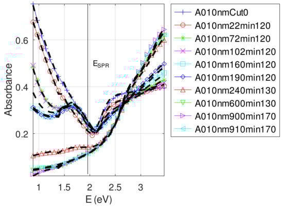
Figure A1.
Absorbance as a function of the photon energy: experimental (black dashed) and best calculated solution (color) for each oxidized sample (initial thickness nm).
Figure A1.
Absorbance as a function of the photon energy: experimental (black dashed) and best calculated solution (color) for each oxidized sample (initial thickness nm).
Figure A2.
Real part of the relative permittivity of copper as a function of the photon energy: bulk (black) and best calculated (color) for each oxidized sample (initial thickness nm).
Figure A2.
Real part of the relative permittivity of copper as a function of the photon energy: bulk (black) and best calculated (color) for each oxidized sample (initial thickness nm).
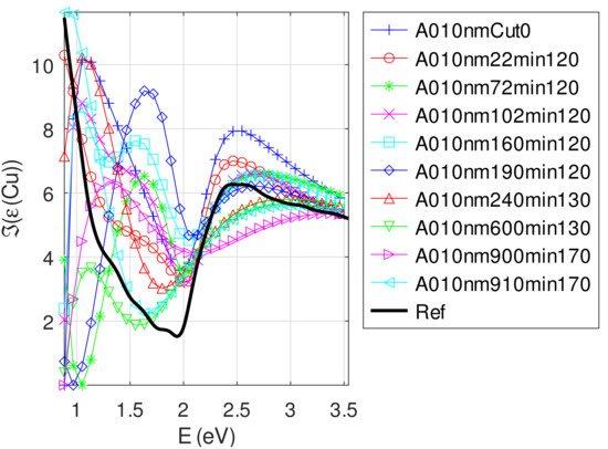
Figure A3.
Imaginary part of the relative permittivity of copper as a function of the photon energy: bulk (black) and best calculated (color) for each oxidized sample (initial thickness nm).
Figure A3.
Imaginary part of the relative permittivity of copper as a function of the photon energy: bulk (black) and best calculated (color) for each oxidized sample (initial thickness nm).

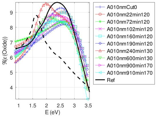
Figure A4.
Real part of the relative permittivity of oxide as a function of the photon energy: bulk Cu2O (black solid line), bulk CuO (black dashed line) and best calculated (color) for each oxidized sample (initial thickness nm).
Figure A4.
Real part of the relative permittivity of oxide as a function of the photon energy: bulk Cu2O (black solid line), bulk CuO (black dashed line) and best calculated (color) for each oxidized sample (initial thickness nm).
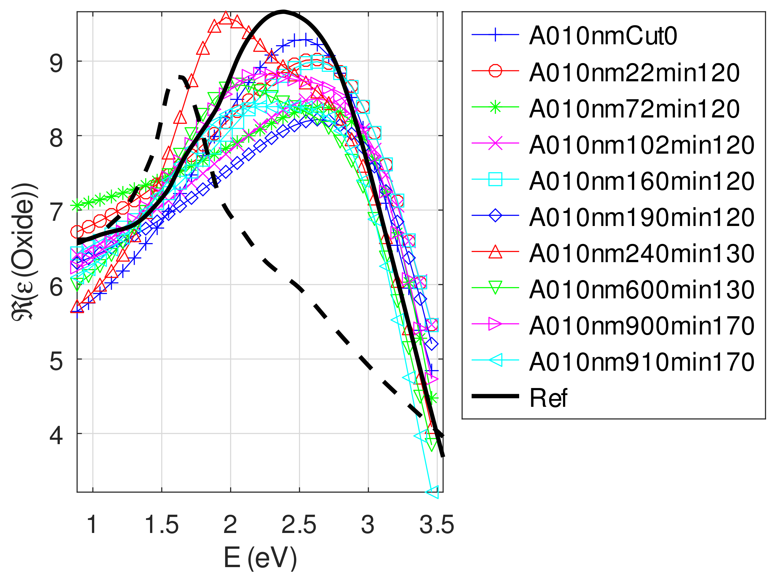
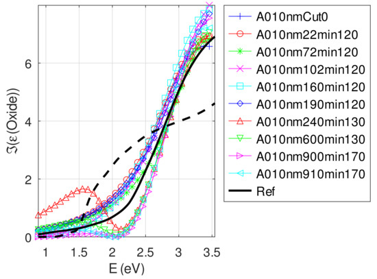
Figure A5.
Imaginary part of the relative permittivity of oxide as a function of the photon energy: bulk Cu2O (black solid line), bulk CuO (black dashed line) and best calculated (color) for each oxidized sample (initial thickness nm).
Figure A5.
Imaginary part of the relative permittivity of oxide as a function of the photon energy: bulk Cu2O (black solid line), bulk CuO (black dashed line) and best calculated (color) for each oxidized sample (initial thickness nm).

Appendix C.4.2. Sample of Initial Copper Thickness nm
Table A4 shows that the least efficient fittings are obtained for the sample with an annealing time greater than 240 min: it is about twice the best value considering all samples. Therefore, the visual inspection of Figure A6 reveals a good quality of fit. Again, the bad tuning of PSO could explain the superiority of ABC+NM and EM+NM. Let us note that neither of the Gradient (+GR) hybridized methods succeeded in reaching the best parameter set. The thickness of copper decreases gently up to the two last annealings. The results obtained after 900 and 910 min are in agreement: only copper oxide remains.
As for the previous sample (with an initial target thickness of 10 nm), the thickness of the raw sample A030nmCut0 was measured with AFM (31 ± 5) nm [14]. We found (30.0 ± 0.1) nm, which is in agreement. The thickness of the fully oxidized sample A030nm900min170 was also measured by AFM: 98 ± 23 nm. Our result is about half of this value. This is probably due to the grain material structure of oxide, which increases the true thickness compared to the effective thickness we calculate. The negative real part of the permittivity of copper is smaller than that of bulk at nm ( eV). Its imaginary part is about seven times greater than that of bulk. Figure A8 shows a global behavior similar to that of thinner copper layers: for small photon energies, the imaginary part of the permittivity is smaller than that of bulk, contrary to the greater photon energies (toward 3.54 eV). Let us note that in the case of total oxidation (900, 910 min), the results for the optical properties of copper are not significant.
Figure A9 shows the same behavior as in Figure A4. The real part of the permittivity of copper oxide is smaller than that of bulk Cu2O for small oxide thicknesses and tends toward the bulk one for thick layers (at nm ( eV)). For thin copper oxide layers, the imaginary part of the permittivity is greater than that of bulk on the whole domain of photon energies. In the case of total oxidation (900–910 min), the real part is much smaller than that of bulk, and the shape of the curve is modified. This behavior is probably due to the inclusion of air in the thick oxide layers. Again, the permittivity remains far from that of CuO.
Table A4.
The recovered thickness of copper and Cooper oxide, the relative permittivity of copper and copper oxide at nm, by fitting experimental UV-visible-NIR absorbance curves. The recovered relative permittivities can be compared to those of bulk copper and copper oxide, resp. −11.55 + 1.57 and 8.64 + 0.64 [29]. The value of the multi-objective function F (Equation (A3)) and the most efficient metaheuristics are also indicated. Values between brackets are standard deviation for acceptable solutions, i.e., obtained for F below the 25% threshold (for . The corresponding success of each metaheuristic is indicated in percentages).
| Sample | F | Method | ||||
|---|---|---|---|---|---|---|
| (nm) | (nm) | at eV | at eV | |||
| A030nmCut0 | 30.0 | 0.0 | −14.1 + 2.7 | 8.3 + 1.2 | 8.7 × 10 | ABC + NM |
| (0.1) | (0.7) | (0.5 + 0.6) | (0.2 + 0.3) | (4 × 10) | ||
| 62%, 38%, 0%, 100%, 0 | ||||||
| A030nm22min120 | 29.9 | 0.1 | −13.3 + 2.8 | 8.6 + 0.7 | 7.9 × 10 | ABC + NM |
| (0.1) | (0.5) | (0.5 + 0.5) | (0.3 + 0.3) | (8 × 10) | ||
| 42%, 50%, 8%, 100%, 0 | ||||||
| A030nm72min120 | 29.5 | 1.0 | −12.5 + 2.9 | 8.2 + 1.0 | 6.2 × 10 | EM + NM |
| (0.3) | (0.5) | (0.4 + 0.4) | (0.3 + 0.3) | (4 × 10) | ||
| 44%, 56%, 0%, 100%, 0 | ||||||
| A030nm102min120 | 29.4 | 1.0 | −13.0 + 2.0 | 8.1 + 1.1 | 5.2 × 10 | EM + NM |
| (0.4) | (0.7) | (0.5 + 0.3) | (0.3 + 0.2) | (5 × 10) | ||
| 14%, 86%, 0%, 100%, 0 | ||||||
| A030nm160min120 | 28.2 | 3.1 | −12.8 + 3.1 | 8.3 + 0.5 | 4.9 × 10 | ABC + NM |
| (0.6) | (1.0) | (0.5 + 0.5) | (0.3 + 0.3) | (5 × 10) | ||
| 17%, 83%, 0%, 100%, 0 | ||||||
| A030nm190min120 | 27.9 | 3.5 | −13.5 + 2.9 | 8.4 + 0.6 | 4.8 × 10 | ABC + NM |
| (0.7) | (1.2) | (0.5 + 0.5) | (0.3 + 0.3) | (5 × 10) | ||
| 50%, 50%, 0%, 100%, 0 | ||||||
| A030nm240min130 | 21.2 | 14.5 | −11.3 + 8.2 | 7.7 + 1.3 | 1.1 × 10 | EM + NM |
| (1.5) | (2.4) | (1.1 + 1.5) | (0.9 + 1.1) | (5 × 10) | ||
| 9%, 70%, 21%, 100%, 0 | ||||||
| A030nm600min130 | 20.1 | 16.6 | −15.9 + 6.8 | 7.7 + 0.6 | 1.2 × 10 | EM + NM |
| (1.2) | (2.2) | (0.9 + 0.8) | (0.9 + 0.6) | (5 × 10) | ||
| 18%, 57%, 25%, 100%, 0 | ||||||
| A030nm900min170 | 0.6 | 44.8 | −10.2 + 2.2 | 7.0 + 0.0 | 1.1 × 10 | EM + NM |
| (4.2) | (6.6) | (0.9 + 1.0) | (1.1 + 0.8) | (5 × 10) | ||
| 4%, 96%, 0%, 100%, 0 | ||||||
| A030nm910min170 | 0.4 | 45.8 | −11.5 + 3.1 | 7.1 + 0.0 | 1.1 × 10 | EM + NM |
| (4.2) | (6.6) | (0.9 + 1.0) | (1.1 + 0.8) | (5 × 10) | ||
| 0%, 40%, 60%, 100%, 0 | ||||||
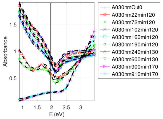
Figure A6.
Absorbance as a function of the photon energy: experimental (black dashed) and best calculated solution (color) for each oxidized sample (initial thickness nm).
Figure A6.
Absorbance as a function of the photon energy: experimental (black dashed) and best calculated solution (color) for each oxidized sample (initial thickness nm).

Table A5.
The recovered thickness of copper and copper oxide, and the relative permittivity of copper and copper oxide at nm, by fitting experimental UV-visible-NIR absorbance curves. The recovered relative permittivities can be compared to those of bulk copper and copper oxide, resp. −11.55 + 1.57 and 8.64 + 0.64 [29]. The value of the multi-objective function F (Equation (A3)) and the most efficient metaheuristics are also indicated. Values between brackets are standard deviation for acceptable solutions, i.e., obtained for F below 25% threshold (for . The corresponding success of each metaheuristic is indicated in percentages).
| Sample | F | Method | ||||
|---|---|---|---|---|---|---|
| (nm) | (nm) | at eV | at eV | |||
| A050nmCut0 | 50.0 | 0.1 | −15.4 + 2.0 | 7.9 + 1.0 | 1.0 × 10 | EM + NM |
| (0.1) | (0.2) | (0.5 + 0.4) | (0.4 + 0.3) | (5 × 10) | ||
| 38%, 62%, 0%, 100%, 0 | ||||||
| A050nm22min120 | 49.8 | 0.1 | −14.6 + 1.8 | 8.2 + 0.8 | 9.3 × 10 | EM + NM |
| (0.1) | (0.2) | (0.4 + 0.4) | (0.3 + 0.3) | (9 × 10) | ||
| 26%, 48%, 26%, 100%, 0 | ||||||
| A050nm72min120 | 49.8 | 0.6 | −14.2 + 2.2 | 8.3 + 0.9 | 7.0 × 10 | EM + NM |
| (0.3) | (0.3) | (0.4 + 0.4) | (0.3 + 0.3) | (4 × 10) | ||
| 33%, 51%, 15%, 100%, 0 | ||||||
| A050nm102min120 | 49.8 | 0.6 | −13.2 + 2.3 | 8.8 + 0.5 | 5.7 × 10 | EM + NM |
| (0.3) | (0.3) | (0.3 + 0.5) | (0.3 + 0.3) | (7 × 10) | ||
| 33%, 56%, 11%, 100%, 0 | ||||||
| A050nm160min120 | 49.2 | 1.6 | −12.5 + 2.3 | 8.4 + 0.8 | 5.6 × 10 | EM + NM |
| (0.5) | (0.6) | (0.4 + 0.4) | (0.3 + 0.2) | (4 × 10) | ||
| 38%, 59%, 3%, 100%, 0 | ||||||
| A050nm190min120 | 49.1 | 1.8 | −12.2 + 2.3 | 8.3 + 0.7 | 5.5 × 10 | EM + NM |
| (0.5) | (0.6) | (0.4 + 0.4) | (0.3 + 0.2) | (3 × 10) | ||
| 43%, 57%, 0%, 100%, 0 | ||||||
| A050nm240min130 | 42.1 | 14.1 | −13.7 + 2.6 | 7.4 + 1.3 | 7.1 × 10 | PSO + NM |
| (3.0) | (5.5) | (0.8 + 0.7) | (0.4 + 0.4) | (9 × 10) | ||
| 0%, 38%, 62%, 100%, 0 | ||||||
| A050nm600min130 | 39.0 | 19.0 | −14.4 + 3.5 | 8.1 + 1.4 | 8.4 × 10 | PSO + NM |
| (3.8) | (6.7) | (1.0 + 0.8) | (0.3 + 0.7) | (1 × 10) | ||
| 29%, 31%, 40%, 97%, 3 | ||||||
| A050nm900min170 | 0.4 | 81.9 | −9.1 + 2.3 | 6.1 + 0.1 | 1.4 × 10 | EM + NM |
| (0.6) | (4.6) | (0.9 + 1.1) | (0.5 + 0.1) | (1 × 10) | ||
| 7%, 83%, 11%, 100%, 0 | ||||||
| A050nm910min170 | 0.0 | 89.6 | −11.5 + 2.8 | 6.6 + 0.3 | 1.4 × 10 | ABC + NM |
| (0.6) | (4.4) | (0.8 + 1.1) | (0.5 + 0.1) | (8 × 10) | ||
| 97%, 0%, 3%, 100%, 0 | ||||||

Figure A7.
Real part of the relative permittivity of copper as a function of the photon energy: bulk (black) and best calculated (color) for each oxidized sample (initial thickness nm).
Figure A7.
Real part of the relative permittivity of copper as a function of the photon energy: bulk (black) and best calculated (color) for each oxidized sample (initial thickness nm).
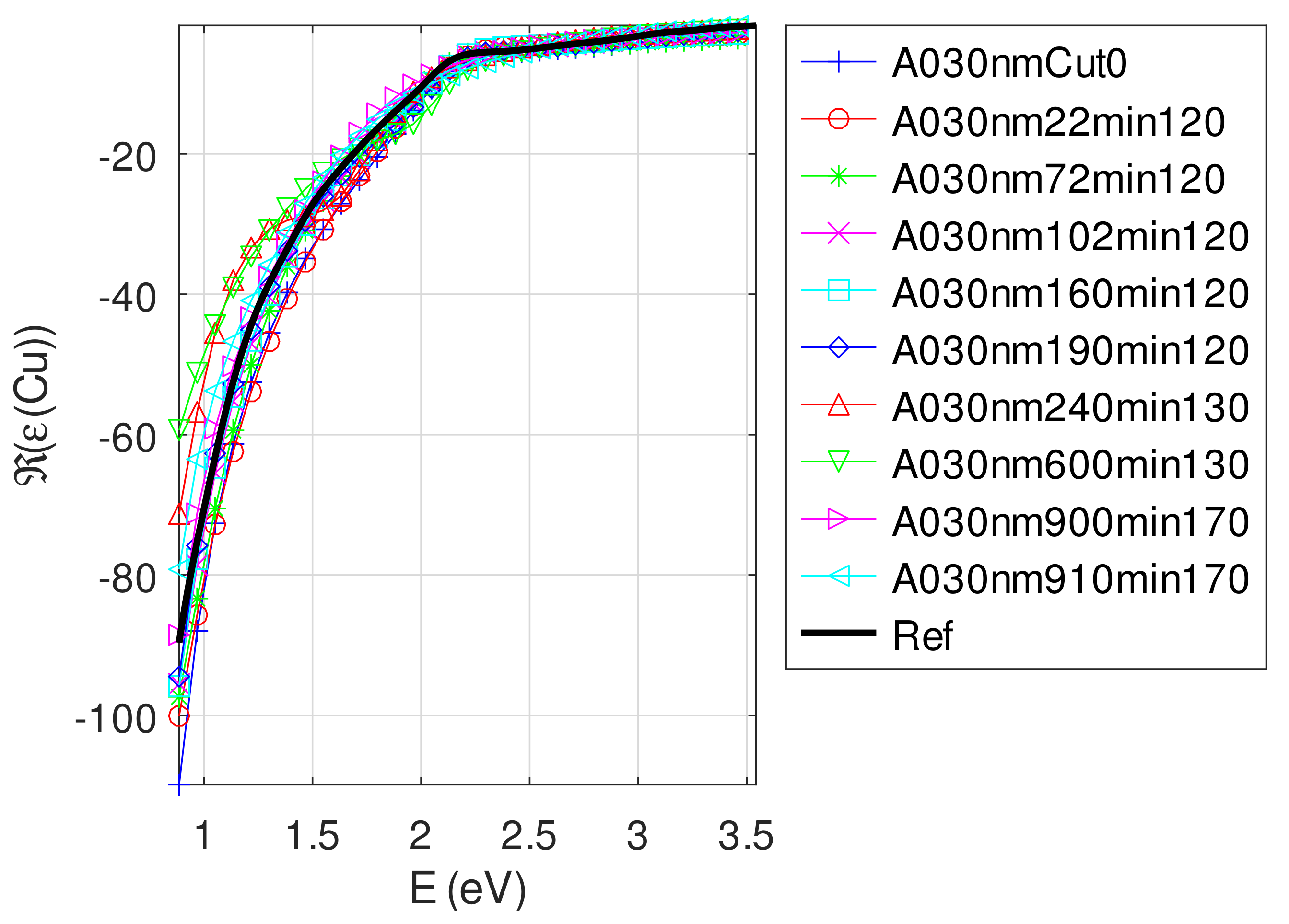
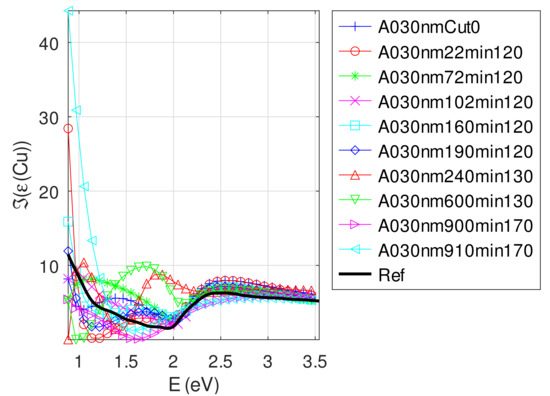
Figure A8.
Imaginary part of the relative permittivity of copper as a function of the photon energy: bulk (black) and best calculated (color) for each oxidized sample (initial thickness nm).
Figure A8.
Imaginary part of the relative permittivity of copper as a function of the photon energy: bulk (black) and best calculated (color) for each oxidized sample (initial thickness nm).
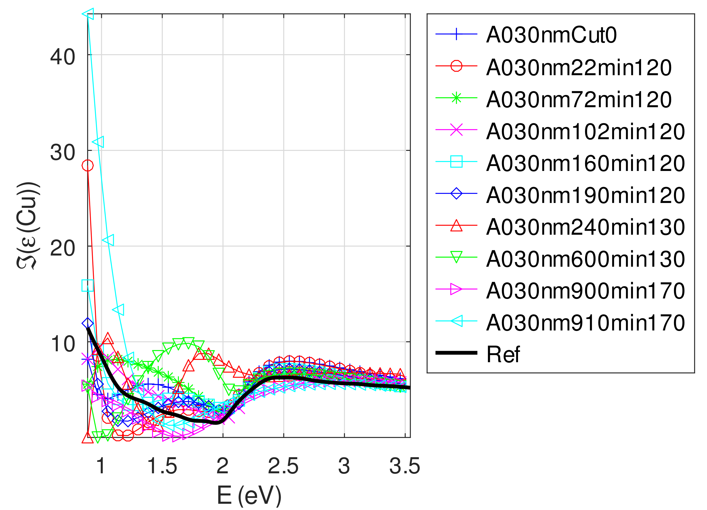
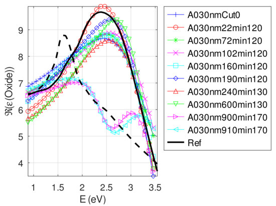
Figure A9.
Real part of the relative permittivity of oxide as a function of the photon energy: bulk Cu2O (black solid line), bulk CuO (black dashed line) and best calculated (color) for each oxidized sample (initial thickness nm).
Figure A9.
Real part of the relative permittivity of oxide as a function of the photon energy: bulk Cu2O (black solid line), bulk CuO (black dashed line) and best calculated (color) for each oxidized sample (initial thickness nm).
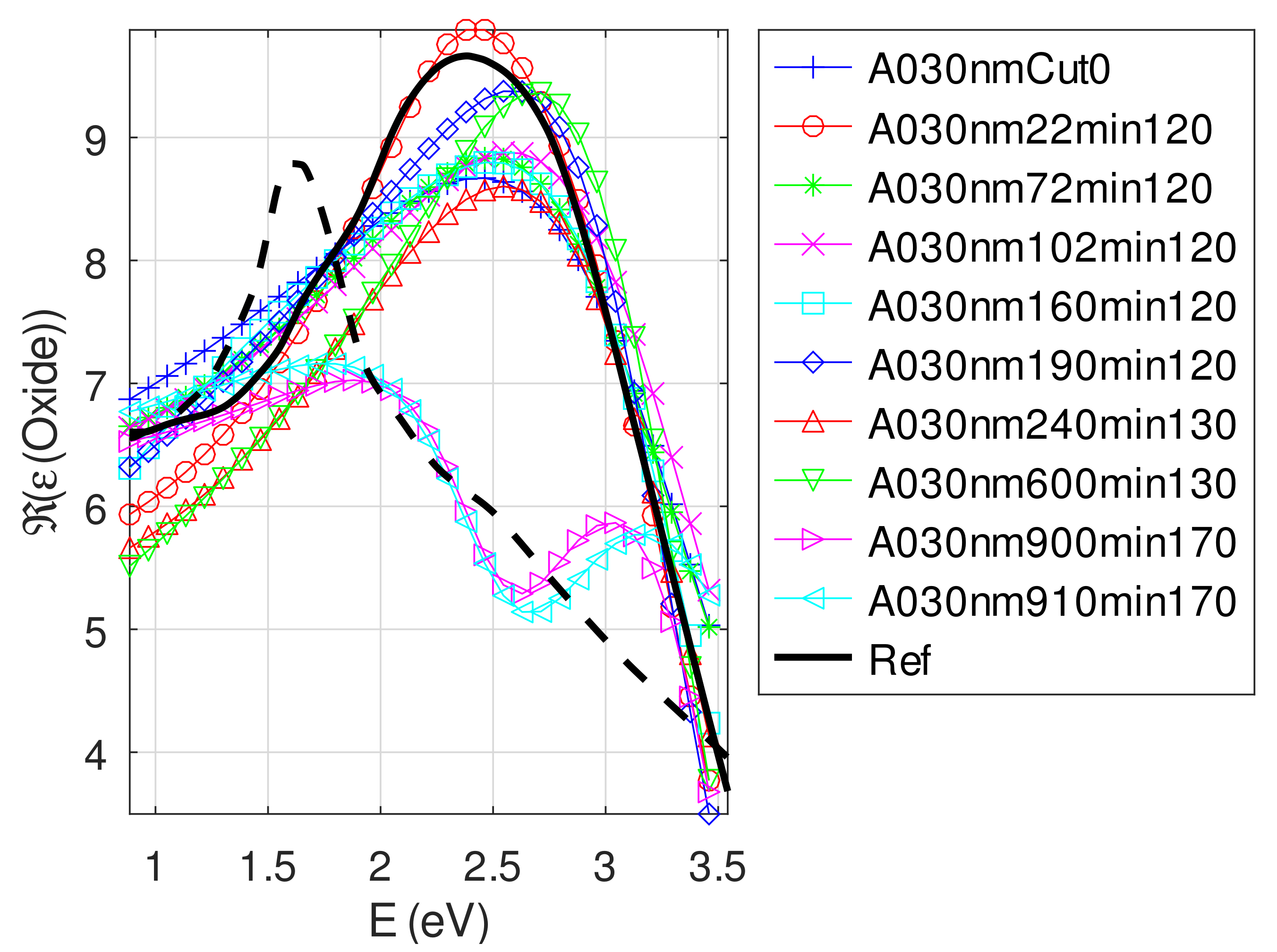
Figure A10.
Imaginary part of the relative permittivity of oxide as a function of the photon energy: bulk Cu2O (black solid line), bulk CuO (black dashed line) and best calculated (color) for each oxidized sample (initial thickness nm).
Figure A10.
Imaginary part of the relative permittivity of oxide as a function of the photon energy: bulk Cu2O (black solid line), bulk CuO (black dashed line) and best calculated (color) for each oxidized sample (initial thickness nm).
Appendix C.4.3. Sample of Initial Copper Thickness nm
Table A5 gives values of the multi-objective function F that are close to those obtained for the other samples. The stability of the methods also is of the same order of magnitude (smaller than 1 × 10). The ABC + NM is the most efficient method even if . The PSO is more efficient for oxidized samples. The thickness of the raw sample A050nmCut0 was measured with AFM (51 ± 8) nm [14]. We found (50.1 ± 0.2) nm, which is in agreement. The thickness of the fully oxidized sample A050nm900min170 also was measured by AFM: 142 ± 30 nm. We found 82.3 ± 4.4 nm. As for the A030nm sample, we found a smaller value. The real part of the permittivity is about 50% smaller than that of the bulk, even for quasi non-oxidized samples. The oxidation appears to be slow to get going. This finding is coherent with that for the two previous samples. The relative permittivity of oxide at eV appears to get closer to that of bulk, except for the two last samples. In these cases, the air inclusions in oxide may explain the strong decay seen in Figure A14. The increase in the imaginary part of the copper permittivity at small photon energies is clear in Figure A13, but for small thicknesses. In the same region of photon energies, the decrease in the real part is similar to that of the two previous samples.
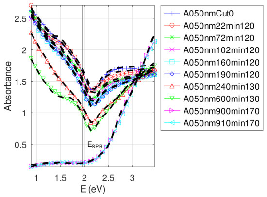
Figure A11.
Absorbance as a function of the photon energy: experimental (black dashed) and best calculated solution (color) for each oxidized sample (initial thickness nm).
Figure A11.
Absorbance as a function of the photon energy: experimental (black dashed) and best calculated solution (color) for each oxidized sample (initial thickness nm).
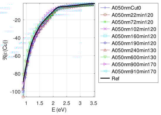
Figure A12.
Real part of the relative permittivity of copper as a function of the photon energy: bulk (black) and best calculated (color) for each oxidized sample (initial thickness nm).
Figure A12.
Real part of the relative permittivity of copper as a function of the photon energy: bulk (black) and best calculated (color) for each oxidized sample (initial thickness nm).
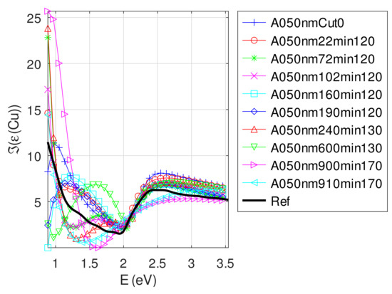
Figure A13.
Imaginary part of the relative permittivity of copper as a function of the photon energy: bulk (black) and best calculated (color) for each oxidized sample (initial thickness nm).
Figure A13.
Imaginary part of the relative permittivity of copper as a function of the photon energy: bulk (black) and best calculated (color) for each oxidized sample (initial thickness nm).
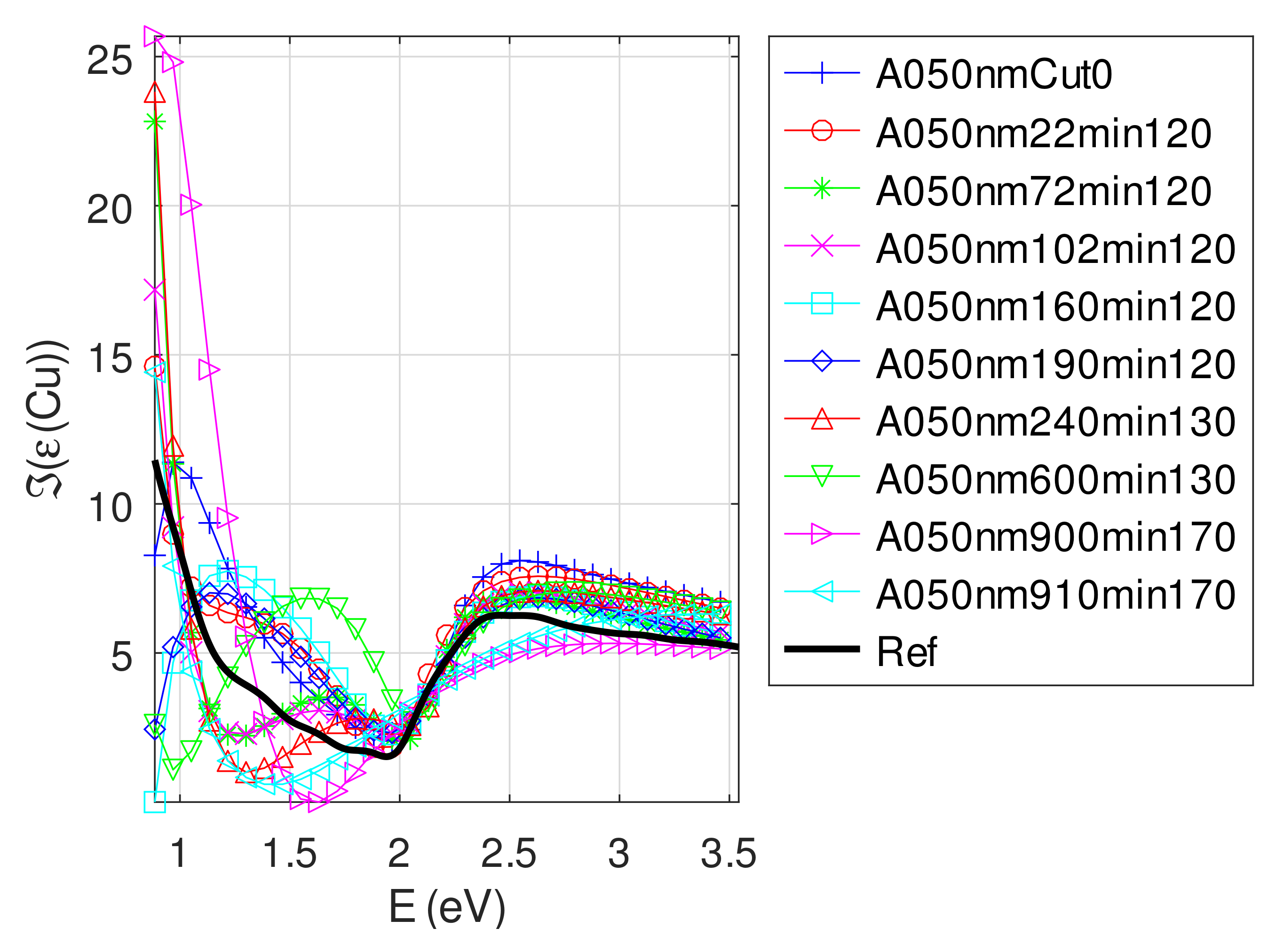

Figure A14.
Real part of the relative permittivity of oxide as a function of the photon energy: bulk Cu2O (black solid line), bulk CuO (black dashed line) and best calculated (color) for each oxidized sample (initial thickness nm).
Figure A14.
Real part of the relative permittivity of oxide as a function of the photon energy: bulk Cu2O (black solid line), bulk CuO (black dashed line) and best calculated (color) for each oxidized sample (initial thickness nm).
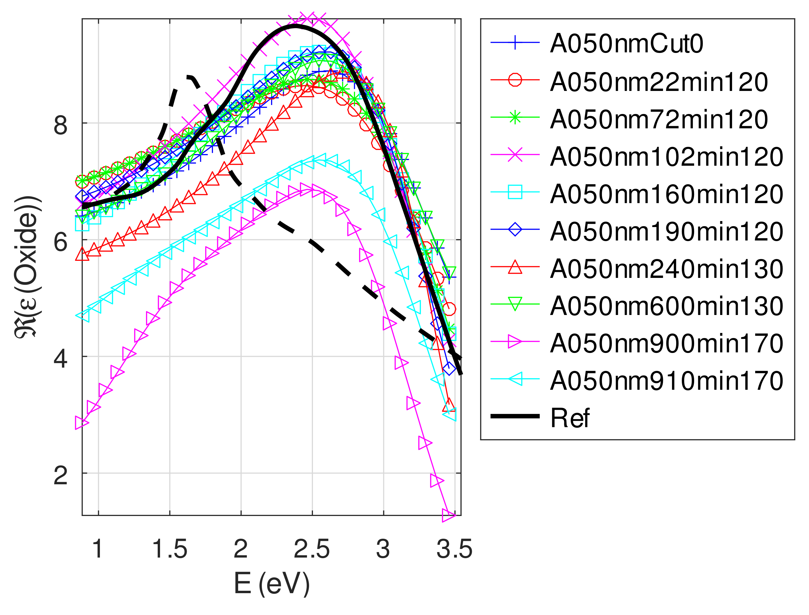
Figure A15.
Imaginary part of the relative permittivity of oxide as a function of the photon energy: bulk Cu2O (black solid line), bulk CuO (black dashed line) and best calculated (color) for each oxidized sample (initial thickness nm).
Figure A15.
Imaginary part of the relative permittivity of oxide as a function of the photon energy: bulk Cu2O (black solid line), bulk CuO (black dashed line) and best calculated (color) for each oxidized sample (initial thickness nm).

Appendix C.5. Discussion on the Resolution of the Inverse Problem: The Fitting of UV-Visible-NIR Absorbance Curves
We used three metaheuristics to recover both thicknesses and optical properties of copper and copper oxide. ABC is globally the most efficient for thin layers, EM takes the second place, and PSO may succeed for oxidized samples. The hybridization with NM is the most efficient in all cases. Let us note that the success of each metaheuristic depends on the tuning of its exogenous parameters. In our case, the fitting requires input parameters for the model; therefore, the fitting may be considered a hard problem. In this case, the “no free lunch theorem” can apply, the topology of the model being dependent on the balance between copper and copper oxide thicknesses [54]. Indeed, two metaheuristics are equivalent if their performances are comparable for all possible problems. Therefore, the resolution of a difficult inverse problem would require more than one metaheuristic to ensure the best result. The repeated realizations of the same algorithm and the use of a tolerance threshold for the values multi-objective function (here 25%) help assess the stability of the methods and the relevance of the outcome [55]. Using this careful approach leads to better results than those found in Reference [15]. The values obtained independently, for all samples, with the same tuning of optimization methods are physically sound.
The electromagnetic model of a plane multilayer combined with partial fraction models for copper (order 4) and oxide (order 2) allow fast calculation and seems to be sufficient to describe the oxidation of thin layers of copper. Actually, the roughness of the layers is small enough [14], and the possible air inclusion in thick oxide layers is reflected in the partial fraction model (Figure A9 and Figure A14).
The model reproduces the dips in UV-visible-NIR absorbance curves. The main one in absorbance curves is close to 2.1 eV and characteristic of the inter-band transition from d states (valence band) to ‘s-p’ conduction bands [18] (Figure A1, Figure A6 and Figure A11). The low boundary of photon energy is greater than the bandgap characteristic of the copper structure [56]. Figure A3, Figure A8 and Figure A13 show a global offset of the relative permittivity of copper relative to the bulk one, especially at low energies: the imaginary part is much smaller. On the contrary, copper is a more absorbing material at higher photon energies. The second dip near 1.25–1.4 eV in Figure A1 and Figure A6 appears for thicknesses of copper and oxide of the same order of magnitude. In this case, the dip reveals the indirect gap of CuO. It disappears for complete oxidation, for which Cu2O dominates. The observed bandgap near 2 and 2.2 eV are not those for CuO observed at a higher temperature of annealing (623 K) [57] but are closer to that of Cu2O (near 2.1 eV) [56]). The slope change in absorbance of pure oxide samples appears near 2.2–2.4 eV and does not indicate a weakened CuO bandgap [57] but the Cu2O bandgap near 2.5 eV [13,58]. This last reference separates CuO and Cu2O bandgaps (respectively, 1.4–1.5 and 2.5 eV). Our results are intermediate between those in Reference [56] (2.1 eV) and [13,58] (2.5 eV) and are coherent with those in Reference [36]. This result is confirmed in Reference [59]: copper oxide phases are mainly Cu2O at oxidation temperature below 400 °C for complete oxidation. CuO remains in the first oxidation steps. This inter-band transition peak (Cu2O) appears and increases with both temperature and oxidation time. However, this latter is attenuated for increasing copper thicknesses. Indeed, for smaller thicknesses (<10 nm), the electric field is stronger. Therefore, the movement of Cu+ ions through the oxide toward the reaction zone is impeded. For nm, the effect of the electric field decreases, and the diffusion of the cations become limited. The optical property of copper oxide moves closer to the CuO bulk at low photon energies. For high photon energies, the imaginary part of the relative permittivity of oxide is greater than that of bulk Cu2O. This may be due to the outbreak of nanoparticles (NPs) of Cu2O, which red-shifts the dips.
References
- Kretschmann, E.; Raether, H. Radiative Decay of Nonradiative Surface Plasmons Excited by Light. Z. Naturforsch. A 1968, 23A, 2135–2136. [Google Scholar] [CrossRef]
- Ahn, H.; Song, H.; Choi, J.R.; Kim, K. A Localized Surface Plasmon Resonance Sensor Using Double-Metal-Complex Nanostructures and a Review of Recent Approaches. Sensors 2018, 18, 98. [Google Scholar] [CrossRef] [PubMed] [Green Version]
- Chen, Z.; Zhao, X.; Lin, C.; Chen, S.; Yin, L.; Ding, Y. Figure of merit enhancement of surface plasmon resonance sensors using absentee layer. Appl. Opt. 2016, 55, 6832–6835. [Google Scholar] [CrossRef] [PubMed]
- Meng, Q.Q.; Zhao, X.; Lin, C.Y.; Chen, S.J.; Ding, Y.C.; Chen, Z.Y. Figure of Merit Enhancement of a Surface Plasmon Resonance Sensor Using a Low-Refractive-Index Porous Silica Film. Sensors 2017, 17, 1846. [Google Scholar] [CrossRef]
- Lee, S.; Kim, J.Y.; Lee, T.W.; Kim, W.K.; Kim, B.S.; Park, J.H.; Bae, J.S.; Cho, Y.C.; Kim, J.; Oh, M.W.; et al. Fabrication of high-quality single-crystal Cu thin films using radio-frequency sputtering. Sci. Rep. 2014, 4, 6230. [Google Scholar] [CrossRef] [Green Version]
- Tripathi, A.; Dixit, T.; Agrawal, J.; Singh, V. Bandgap engineering in CuO nanostructures: Dual-band, broadband, and UV-C photodetectors. Appl. Phys. Lett. 2020, 116, 111102. [Google Scholar] [CrossRef]
- Editorial Feature of AEO Nano. Copper (Cu) Nanoparticles-Properties, Applications. Available online: https://www.azonano.com/article.aspx?ArticleID=3271 (accessed on 9 May 2021).
- Kesarwani, R.; Khare, A. Surface plasmon resonance and nonlinear optical behavior of pulsed laser-deposited semitransparent nanostructured copper thin films. Appl. Phys. B 2018, 124, 116. [Google Scholar] [CrossRef]
- Rodrigues, E.P.; Oliveira, L.C.; Silva, M.L.F.; Moreira, C.S.; Lima, A.M.N. Surface Plasmon Resonance Sensing Characteristics of Thin Copper and Gold Films in Aqueous and Gaseous Interfaces. IEEE Sens. J. 2020, 20, 7701–7710. [Google Scholar] [CrossRef]
- Stebunov, Y.V.; Yakubovsky, D.I.; Fedyanin, D.Y.; Arsenin, A.V.; Volkov, V.S. Superior Sensitivity of Copper-Based Plasmonic Biosensors. Langmuir 2018, 34, 4681–4687. [Google Scholar] [CrossRef] [Green Version]
- Granito, C.; Wilde, J.; Petty, M.; Houghton, S.; Iredale, P. Toluene vapour sensing using copper and nickel phthalocyanine Langmuir-Blodgett films. Thin Solid Films 1996, 284–285, 98–101. [Google Scholar] [CrossRef]
- Homola, J.; Yee, S.S.; Gauglitz, G. Surface Plasmon Resonance Sensors Review. Sens. Actuators B 1999, 54, 3–15. [Google Scholar] [CrossRef]
- Murali, D.S.; Kumar, S.; Choudhary, R.J.; Wadikar, A.D.; Jain, M.K.; Subrahmanyam, A. Synthesis of Cu2O from CuO thin films: Optical and electrical properties. Int. Adv. Eng. Res. Sci. (IJAERS) 2015, 5, 047143. [Google Scholar] [CrossRef]
- Cakir, D. Enhanced Raman Signatures on Copper Based-Materials. Ph.D. Thesis, Univesité de Montpellier, Montpellier, France, 2017. [Google Scholar]
- Barchiesi, D.; Cakir, D.; Grosges, T.; Fréty, N.; Anglaret, E. Recovering effective thicknesses and optical properties of copper and copper oxide layers from absorbance measurements. Opt. Mater. 2019, 91, 138–146. [Google Scholar] [CrossRef]
- Han, L.; Zhou, D.; Li, K.; Xun, l.; Huang, W.P. A Rational-Fraction Dispersion Model for Efficient Simulation of Dispersive Material in FDTD Method. J. Light. Technol. 2012, 30, 2216–2225. [Google Scholar] [CrossRef]
- Michalski, K.A. On the Low-Order Partial-Fraction Fitting of Dielectric Functions at Optical Wavelengths. IEEE Trans. Antennas Propag. 2013, 61, 6128–6135. [Google Scholar] [CrossRef]
- Gharbi, T.; Barchiesi, D.; Kessentini, S.; Maalej, R. Fitting optical properties of metals by Drude-Lorentz and partial-fraction models in the [0.5;/,6] eV range. Opt. Mater. Express 2020, 10, 1129–1162. [Google Scholar] [CrossRef]
- Barchiesi, D.; Otto, A. Excitations of surface plasmon polaritons by attenuated total reflection, revisited. Riv. Nuovo C. 2013, 36, 173–209. [Google Scholar]
- Barchiesi, D.; Kremer, E.; Mai, V.P.; Grosges, T. A Poincaré’s Approach for Plasmonics The Plasmon Localization. J. Microsc. 2008, 229, 525–532. [Google Scholar] [CrossRef]
- Barchiesi, D.; Lidgi-Guigui, N.; Lamy de la Chapelle, M. Functionalization Layer Influence on the Sensitivity of Surface Plasmon Resonance (SPR) Biosensor. Opt. Commun. 2012, 285, 1619–1623. [Google Scholar] [CrossRef]
- Salvi, J.; Barchiesi, D. Measurement of thicknesses and optical properties of thin films from Surface Plasmon Resonance (SPR). Appl. Phys. A 2014, 115, 245–255. [Google Scholar] [CrossRef]
- Kessentini, S.; Barchiesi, D. Nanostructured Biosensors Influence of Adhesion Layer, Roughness and Size on the LSPR A Parametric Study. In State of the Art in Biosensors-General Aspects; Rinken, T., Ed.; INTECH Open Access: London, UK, 2013; Chapter 12; pp. 311–330. ISBN 978-953-51-1004-0. [Google Scholar]
- Colas, F.; Barchiesi, D.; Kessentini, S.; Toury, T.; Lamy de la Chapelle, M. Comparison of adhesion layers of gold on silicate glasses for SERS detection. J. Opt. 2015, 17, 114010. [Google Scholar] [CrossRef] [Green Version]
- Barchiesi, D. A classroom theory of the surface plasmon polariton. Eur. J. Phys. 2012, 33, 1345–1357. [Google Scholar] [CrossRef]
- Lecaruyer, P.; Canva, M.; Rolland, J. Metallic Film Optimization in a Surface Plasmon Resonance Biosensor by the Extended Rouard Method. Appl. Opt. 2007, 46, 2361–2369. [Google Scholar] [CrossRef] [PubMed]
- Barchiesi, D. Improved method based on S matrix for the optimization of SPR biosensors. Opt. Commun. 2013, 286, 23–29. [Google Scholar] [CrossRef]
- Barchiesi, D. Numerical retrieval of thin aluminium layer properties from SPR experimental data. Opt. Express 2012, 20, 9064–9078. [Google Scholar] [CrossRef]
- Software Spectra, I. Optical Data from Sopra SA. Available online: http://www.sspectra.com/sopra.html (accessed on 9 May 2021).
- Ramirez, M.; Henneken, L.; Virtanen, S. Oxidation kinetics of thin copper films and wetting behaviour of copper and Organic Solderability Preservatives (OSP) with lead-free solder. Appl. Surf. Sci. 2011, 257, 6481–6488. [Google Scholar] [CrossRef]
- Shanidand, M.; Abdul Khadar, M.; Sathe, V.G. Fröhlich interaction and associated resonance enhancement in nanostructured copper oxide films. J. Raman Spectrosc. 2011, 42, 1769–1773. [Google Scholar] [CrossRef]
- Figueiredo, V.; Elangovan, E.; Goncalves, G.; Barquinha, P.; Pereira, L.; Franco, N.; Alves, E.; Martins, R.; Fortunato, E. Effect of post-annealing on the properties of copper oxide thin films obtained from the oxidation of evaporated metallic copper. Appl. Surf. Sci. 2008, 254, 3949–3954. [Google Scholar] [CrossRef]
- Gao, W.; Hong, H.; He, J.; Thomas, A.; Chan, L.; Li, S. Oxidation behaviour of Cu thin films on Si wafer at 175–400 °C. Mater. Lett. 2001, 51, 78–84. [Google Scholar] [CrossRef]
- Iijima, J.; Lim, J.W.; Hong, H.S.; Suzuki, S.; Mimura, K.; Isshiki, M. Native oxidation of ultra high purity Cu bulk and thin films. Appl. Surf. Sci. 2006, 253, 2825–2829. [Google Scholar] [CrossRef]
- Cabrera, N.; Mott, N.F. Theory of the oxidation of metals. Rep. Prog. Phys. 1949, 12, 163. [Google Scholar] [CrossRef]
- Mugwang’a, F.; Karimi, P.; Njoroge, W.; Omayio, O.; Waita, S. Optical characterization of Copper Oxide thin films prepared by reactive dc magnetron sputtering for solar cell applications. Int. J. Thin Film Sci. Technol. 2012, 2, 15–24. [Google Scholar]
- Shi, Y.; Eberhart, R.C. A modified particle swarm optimizer. In Proceedings of the IEEE Congress on Evolutionary Computation (CEC’98), Anchorage, Alaska, 4–9 May 1998; pp. 69–73. [Google Scholar]
- Rahmat-Samii, Y. Genetic algorithm (GA) and particle swarm optimization (PSO) in engineering electromagnetics. In Proceedings of the 17th International Conference on Applied Electromagnetics and Communications, Dubrovnik, Republika Hrvatska, 1–3 October 2003; pp. 1–5. [Google Scholar] [CrossRef]
- Robinson, J.; Rahmat-Samii, Y. Particle swarm optimization in electromagnetics. IEEE Trans. Antennas Propag. 2004, 52, 397–407. [Google Scholar] [CrossRef]
- Barchiesi, D. Numerical optimization of plasmonic biosensors. In New Perspectives in Biosensors Technology and Applications; Serra, P.A., Ed.; INTECH Open Access: London, UK, 2011; Chapter 5; pp. 105–126. ISBN 978-953-307-448-1. [Google Scholar]
- Turbadar, T. Complete Absorption of Light by Thin Metal Films. Proc. Phys. Soc. 1959, 73, 40–44. [Google Scholar] [CrossRef]
- Holland, J.H. Adaptation in Natural and Artificial Systems: An Introductory Analysis with Applications to Biology, Control, and Artificial Intelligence; Michigan University: Ann Arbor, MI, USA, 1975. [Google Scholar]
- Bäck, T.; Hammel, U.; Schwefel, H.P. Evolutionary Computation Comments on the History and Current State. IEEE Trans. Evol. Comput. 1997, 1, 3–17. [Google Scholar] [CrossRef] [Green Version]
- Macías, D.; Vial, A.; Barchiesi, D. Evolution Strategies Approach for the Solution of an Inverse Problem in Near-Field Optics. In Lecture Notes in Computer Science (6e European Workshop on Evolutionary Computation in Image Analysis and Signal Processing); Raidl, G., Cagnoni, S., Branke, J., Corne, D.W., Drechsler, R., Jin, Y., Johnson, C., Machado, P., Marchiori, E., Rothlauf, F., et al., Eds.; Springer: Berlin/Heidelberg, Germany, 2004; Volume 3005/2004, pp. 329–338. [Google Scholar]
- Johnson, J.; Rahmat-Samii, V. Genetic algorithms in engineering electromagnetics. IEEE Antennas Propag. Mag. 1997, 39, 7–21. [Google Scholar] [CrossRef] [Green Version]
- Rahmat-Samii, Y.; Michielssen, E. Electromagnetic Optimization by Genetic Algorithms, 1st ed.; John Wiley & Sons, Inc.: Hoboken, NJ, USA, 1999. [Google Scholar]
- Macías, D.; Vial, A.; Barchiesi, D. Application of Evolution Strategies for the Solution of an Inverse Problem in Near-Field Optics. J. Opt. Soc. Am. A 2004, 21, 1465–1471. [Google Scholar] [CrossRef]
- Karaboga, D. An Idea Based on Honey Bee Swarm for Numerical Optimization; Technical Report tr06; Erciyes University, Engineering Faculty, Computer Engineering Department: Kayseri, Turkey, 2005. [Google Scholar]
- Zaman, M.; Gaffar, M.; Alam, M.M.; Mamun, S.; Matin, M. Synthesis of Antenna Arrays Using Artificial Bee Colony Optimization Algorithm. Int. J. Microw. Opt. Technol. 2011, 6, 234–241. [Google Scholar]
- Kessentini, S.; Naãs, I. Absolute versus stochastic stability of the artificial bee colony in synchronous and sequential modes. Natural Comput. 2021, 20, 443–470. [Google Scholar] [CrossRef]
- Chiandussi, G.; Codegone, M.; Ferrero, S.; Varesio, F. Comparison of multi-objective optimization methodologies for engineering applications. Comput. Math. Appl. 2012, 63, 912–942. [Google Scholar] [CrossRef] [Green Version]
- Jiang, M.; Luo, Y.P.; Yang, S.Y. Stochastic convergence analysis and parameter selection of the standard particle swarm optimization algorithm. Inf. Process. Lett. 2007, 102, 8–16. [Google Scholar] [CrossRef]
- Trelea, I.C. The particle swarm optimization algorithm convergence analysis and parameter selection. Inf. Process. Lett. 2003, 85, 317–325. [Google Scholar] [CrossRef]
- Wolpert, D.H.; Macready, W. No Free Lunch Theorems for Optimization. IEEE Trans. Evol. Comput. 1997, 1, 67–82. [Google Scholar] [CrossRef] [Green Version]
- Barchiesi, D.; Grosges, T. Propagation of uncertainties and applications in numerical modeling: Tutorial. J. Opt. Soc. Am. A 2017, 34, 1602–1619. [Google Scholar] [CrossRef] [PubMed] [Green Version]
- Korzhavyi, P.A.; Johansson, B. Literature Review on the Properties of Cuprous Oxide Cu2O and the Process of Copper Oxidation; Technical Report SKB TR-11-08, Svensk Kärnbränslehantering AB; Swedish Nuclear Fueland Waste Management Co.: Stockholm, Sweden, 2011. [Google Scholar]
- Alhassan, W.A.A.; Wadi, I.A. Determination of Optical Energy Gap fo rCopper oxide at Different Temperatures. Int. Adv. Eng. Res. Sci. (IJAERS) 2018, 5, 255–258. [Google Scholar] [CrossRef]
- Wang, Y.; Lany, S.; Ghanbaja, J.; Fagot-Revurat, Y.; Chen, Y.P.; Soldera, F.; Horwat, D.; Mücklich, F.; Pierson, J.F. Electronic structures of Cu2O, Cu4O3, and CuO: A joint experimental and theoretical study. Phys. Rev. B 2016, 94, 245418. [Google Scholar] [CrossRef] [Green Version]
- Hu, Y.Z.; Sharangpani, R.; Tay, S.P. Kinetic investigation of copper film oxidation by spectroscopic ellipsometry and reflectometry. J. Vac. Sci. Technol. A 2000, 18, 2527–2532. [Google Scholar] [CrossRef]
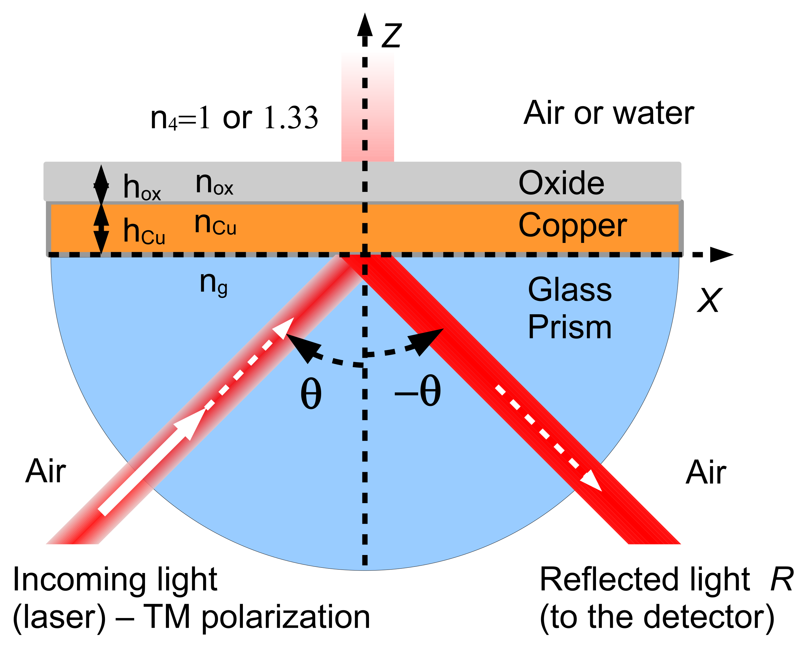
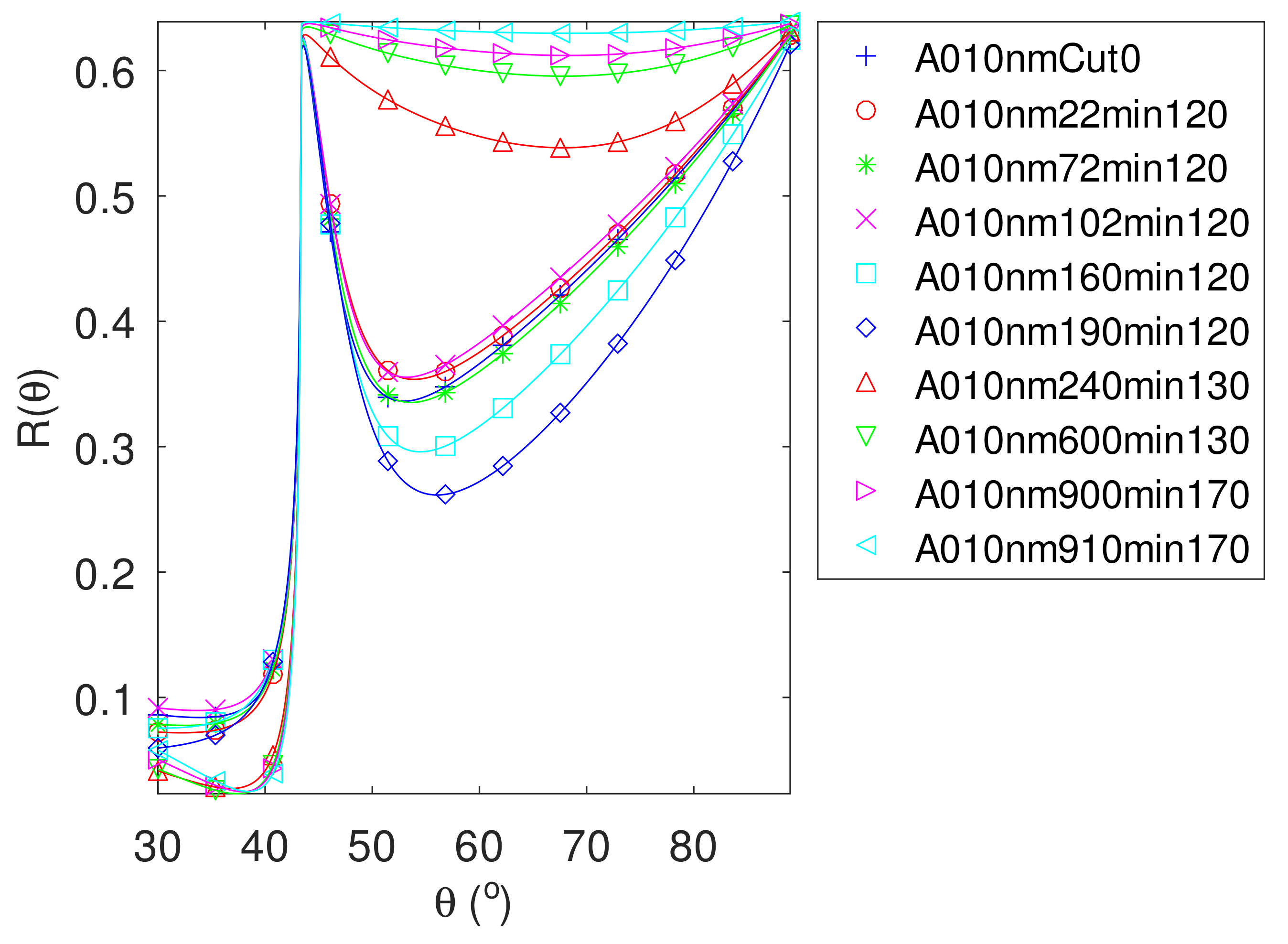
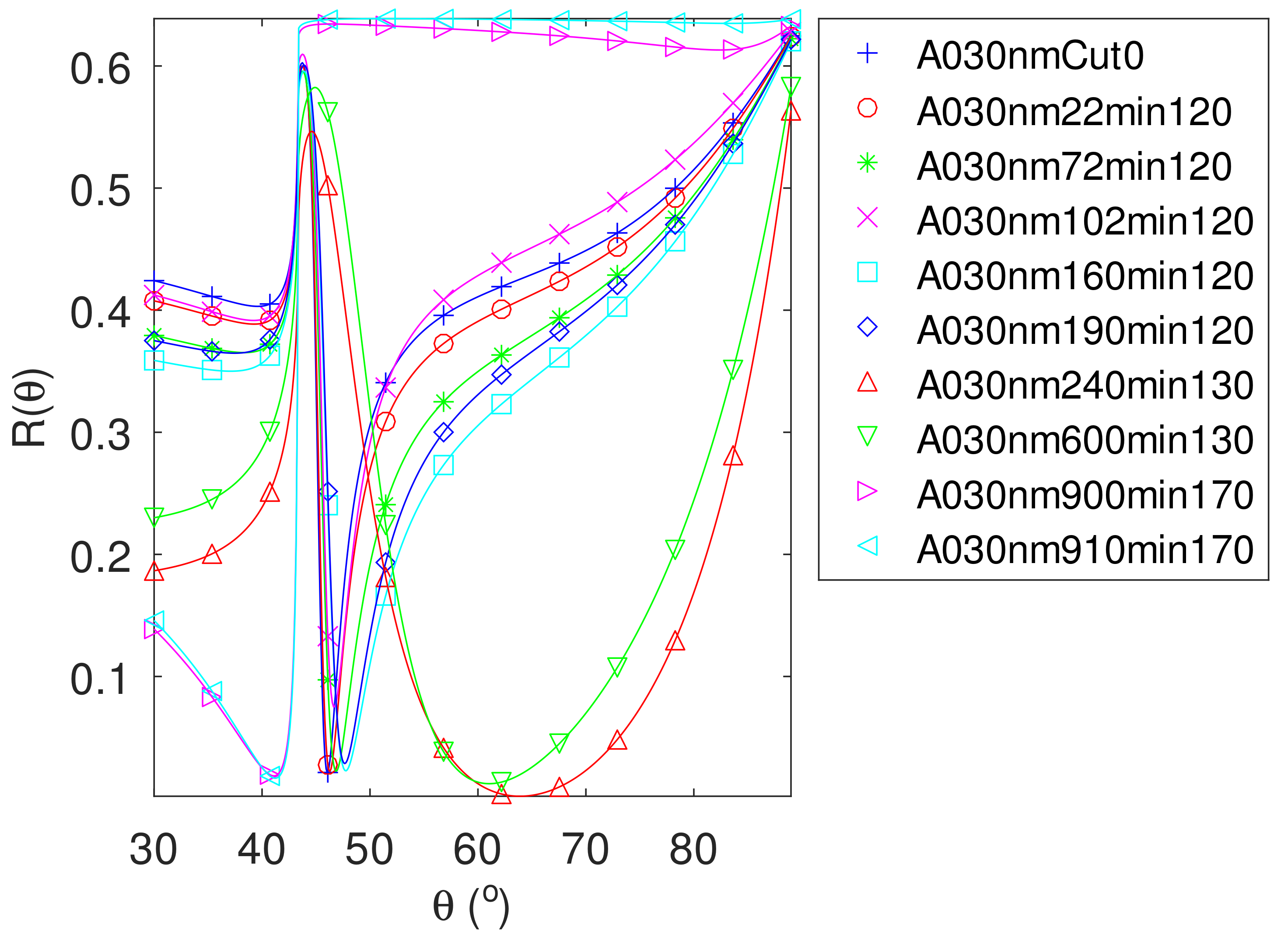
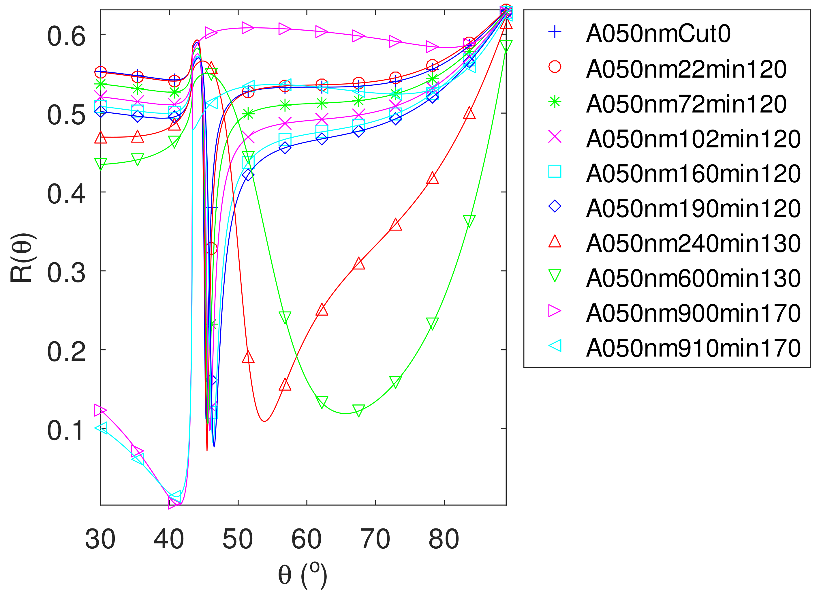
Publisher’s Note: MDPI stays neutral with regard to jurisdictional claims in published maps and institutional affiliations. |
© 2022 by the authors. Licensee MDPI, Basel, Switzerland. This article is an open access article distributed under the terms and conditions of the Creative Commons Attribution (CC BY) license (https://creativecommons.org/licenses/by/4.0/).