1. Introduction
High-speed analog-to-digital converters (ADCs) with large analog bandwidths are urgently required in modern radar and electronic reconnaissance systems, since the carrier frequency and the instantaneous bandwidth of the battlefield signal have been tremendously increased to enhance the combat effectiveness [
1]. Due to the electronic bottleneck in the CMOS technology, the sampling rate and the analog bandwidth of a silicon-based ADC are generally below 10 GSa/s and 10 GHz, respectively, which cannot meet the direct digitization requirement of a broadband microwave or millimeter wave (mmW) signal [
2]. At present, the most common method to digitize a high-frequency signal is employing single- or multiple-stage mixing to down-convert the signal to the intermediate-frequency range and then using an ADC to achieve digitization [
3,
4]. For a broadband signal, a time-interleaved ADC array or even a parallel down-conversion-based channelization architecture must be used, which greatly increases the system complexity and the power consumption. Although the sampling rate and the analog bandwidth of an ADC when using InP or SiGe processes can exceed 100 GSa/s and 70 GHz, respectively, the parallel architecture based on multi-chip interleaving must be utilized, which inevitably introduces large spurious signals due to the inter-channel mismatch.
In recent years, ADCs based on photonic sampling are recognized as a promising candidate to achieve direct digitization of a broadband microwave or mmW signal [
5,
6,
7]. Firstly, the 3-dB modulation bandwidth of an electro-optic modulator used for sampling is larger than 100 GHz based on the thin-film lithium niobate (LNOI) platform, which has the potential to enhance the analog bandwidth of the photonic sampling ADC beyond tens of GHz [
8,
9,
10]. Secondly, the ultra-short optical pulse train generated by using a mode-locked laser or a cavity-less optical pulse source has a pulse width in the picosecond level, a repetition rate in the range of multiple GHz to 40 GHz and a time jitter below tens of femtoseconds, which is beneficial for achieving broadband and high-accuracy sampling with a sampling rate beyond tens of GSa/s [
11,
12,
13,
14]. Thirdly, time and wavelength multiplexing/demultiplexing can be flexibly implemented in the optical domain, which is favorable for realizing speed matching between the fast optical front end and the relatively slow electronic back end [
15,
16,
17]. Although the photonic sampling ADC can achieve direct digitization of a microwave or mmW signal, parallel electronic ADCs must be used for a broadband signal due to the constraint of the Nyquist sampling theorem, which inevitably increases the difficulty of multiple-channel data fusion. Large spurious signals may be generated due to the inter-channel gain and time delay mismatch, which puts a limit to the dynamic range of the ADC system.
Non-uniform sampling is an effective method to break the constraint of the Nyquist sampling theorem, which makes it possible to use a single low-speed ADC to digitize a broadband signal [
18,
19,
20,
21]. Under this condition, spurious signals induced by the inter-channel mismatch can be avoided. Single-channel non-uniform photonic sampling (NPS) can be used to digitize a broadband signal in the frequency range up to tens of GHz, benefiting by the large modulation bandwidth of the electro-optic modulator, the picosecond-level pulse width, and the low time jitter of the optical sampling pulse train. In the NPS, according to the non-uniform sampling strategy, low-speed non-uniform sampling optical pulses with a certain statistical distribution are specifically selected from a high-speed uniform optical pulse train. Based on the preset non-uniform sampling instants and the corresponding reconstruction algorithm, the signal information can be reconstructed from the non-uniform samples, where the retrieved signal information is identical to that obtained by using the original high-speed uniform optical pulse train to achieve sampling. Compared with other sub-Nyquist sampling techniques, such as the one based on time stretch and compressive sensing [
22,
23], the non-uniform sampling technique can be used to digitize continuous-time and full-bandwidth signals but is only suitable for periodic signals.
Several non-uniform sampling strategies and a universal reconstruction algorithm have been proposed in the previous works [
18,
19,
20,
21]. In [
18], the non-uniform sampling optical pulses were formed by randomly selecting one pulse from the middle four pulses of every ten uniform optical pulses. Nevertheless, this sampling strategy is unable to acquire the signal information identical to that obtained through its equivalent high-speed uniform sampling, since some of the optical pulses are blocked throughout the sampling. Hence, it cannot be used to digitize a broadband signal, e.g., a linear frequency modulation (LFM) signal. In [
19], the non-uniform sampling strategy based on additive random sampling was demonstrated to have the ability to digitize any signal with a frequency lower than the Nyquist frequency of its equivalent high-speed uniform sampling. Based on the additive random sampling, two-tone signals were accurately identified over an operation bandwidth up to 80 Nyquist zones [
20]. However, as the signal bandwidth approaches the Nyquist frequency of its equivalent high-speed uniform sampling, the additive random sampling requires a sufficiently long sampling time to guarantee that the probability density function of the sampling instants tends to uniform, which greatly increase the data volume and the sampling time. Therefore, for a broadband signal, the number of the samples based on the additive random sampling strategy is far more than that based on its equivalent high-speed uniform sampling to obtain an identical signal information, which hinders the real-time reconstruction of a broadband signal. In [
21], the digital alias-free signal processing (DASP) algorithm was proposed to reconstruct the signal information from the non-uniform samples, where a matrix with a size equal to the square of the sampling number is required to achieve the signal reconstruction. Limited by the size of the reconstruction matrix and the computation time of its inverse matrix, the DASP algorithm can only be used to process the non-uniform samples with a sampling number below tens of thousands, which puts a limit to the spectral resolution.
In this paper, a novel NPS strategy and its special signal reconstruction algorithm are proposed and verified through numerical simulation. The most prominent advantage of this scheme lies in that a uniform probability density function of the sampling instants can be obtained based on a small sampling number, which greatly reduce the data volume and the sampling time to acquire the signal information identical to that obtained by its equivalent high-speed uniform sampling. In addition, the signal reconstruction speed of the proposed algorithm is millions of times faster than that in [
21]. Based on the proposed scheme, NPS with an average sampling rate of 1 GSa/s is used to digitize a single-tone signal with a frequency of 9.9 GHz and an LFM signal in the frequency range of 1 GHz to 9 GHz. The results fit in with those obtained by using the equivalent high-speed uniform sampling under a sampling rate of 20 GSa/s.
2. Operation Principle
Figure 1 shows the schematic diagram of the single-channel NPS-based ADC system. The system is composed of four main parts, as depicted in the green box. Firstly, a pulse pattern generator (PPG) is used to drive an electro-optic Mach-Zehnder modulator (MZM), which acts as an ultrafast optical switch to select a low-average-speed non-uniform optical pulse train from a high-speed uniform optical pulse train generated by using an ultra-short optical pulse source. The PPG and the MZM are synchronized with each other by using a clock circuit. Then, the non-uniform optical pulse train is divided into two branches via an optical coupler (OC) with a power splitting ratio of 95:5, where the non-uniform optical pulse train in the upper branch with 95% optical power and that in the lower branch with 5% optical power are used to achieve photonic sampling and to generate the sampling clock, respectively. In the part of photonic sampling, the non-uniform optical pulse train is modulated by the input signal via a broadband MZM biased at its quadrature point. Subsequently, two low-speed photodetectors (PDs) are used to achieve photoelectric conversion of the sampled non-uniform optical pulse train and to retrieve the non-uniform electrical sampling clock, respectively. A track-and-hold (T/H) circuit synchronized with the non-uniform electrical sampling clock is used to maintain the voltage level in each sampling duration, which facilitates digitization via an electronic ADC working at the average sampling speed of the non-uniform optical pulse train. Finally, the data stream from the electronic ADC is sent to a field-programmable gate array (FPGA) to achieve signal reconstruction.
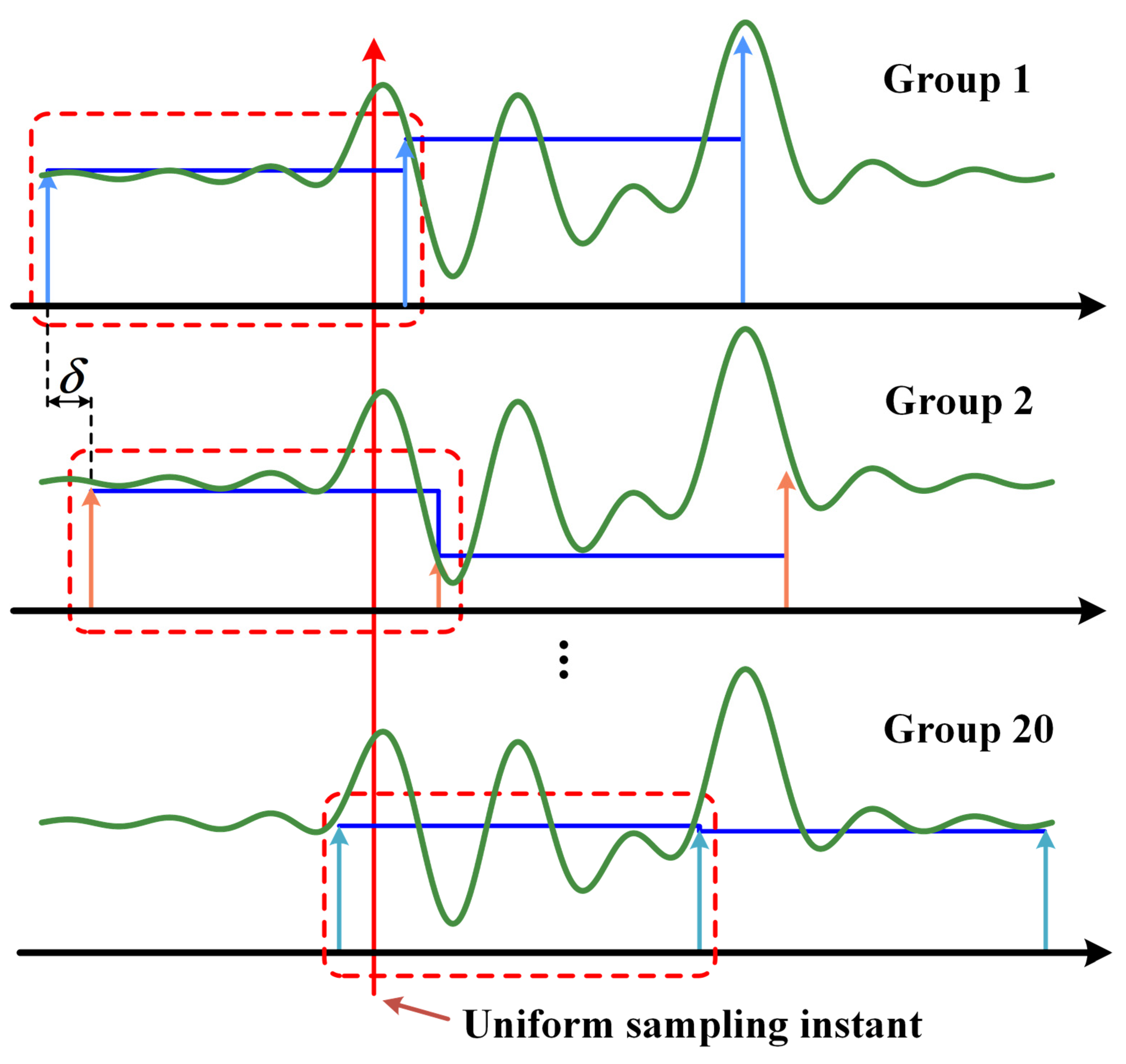
Figure 2 presents the schematic diagram of the proposed NPS strategy. Firstly, the equivalent high-speed uniform optical pulse train with a repetition frequency of
fδ (i.e., an interval of
δ) is divided into
M groups of low-speed uniform optical pulse train with a repetition frequency of
fμ (i.e., an interval of
μ =
Mδ) as depicted in
Figure 2a. In
Figure 2a, the different groups of low-speed uniform optical pulse train are denoted by different colors. Then, the
M groups of low-speed uniform optical pulse train are connected in sequence to form a low-speed non-uniform optical pulse train with an average repetition frequency of
fμ as depicted in
Figure 2b. The interval between the last sampling pulse in the previous group and the first sampling pulse in the next group is
μ +
δ. Therefore, the low-speed non-uniform sampling is equivalent to the high-speed uniform sampling when the time window of the high-speed uniform sampling is equal to an integral multiple of the input signal period. The most prominent advantage of the proposed NPS strategy lies in that the sampling interval between any adjacent non-uniform sampling pulses is enlarged by
M times compared with its equivalent high-speed uniform sampling. Hence, the bandwidth requirement of the back-end devices, such as the PD, the T/H circuit and the electronic ADC, is relaxed by
M/2 times. Compared with the existing NPS schemes, the proposed NPS strategy can greatly reduce the amount of data to maintain the equivalent relationship between the low-speed non-uniform sampling and the high-speed uniform sampling, which is beneficial for improving the signal processing speed. It should be pointed out that the proposed non-uniform sampling strategy can be considered as an extension of the strategy used in the sampling oscilloscope. If
μ is equal to the period of the signal under test, the proposed non-uniform sampling strategy is equivalent to the strategy used in the sampling oscilloscope.
Figure 3 exhibits the flowchart of the signal reconstruction algorithm specially designed for the proposed NPS strategy. Firstly, the low-speed non-uniform samples in
Figure 3a are divided into
M groups of low-speed uniform samples in
Figure 3b according to the NPS strategy. Then, the
M groups of low-speed uniform samples are interleaved to reconstruct the equivalent high-speed uniform samples, as shown in
Figure 3c. The interleaving is essentially an inverse process of the sampling strategy in
Figure 2, where the
M groups of low-speed uniform samples are moved to its original position, as depicted in
Figure 2a. Based on the reconstructed equivalent high-speed uniform samples, the spectral information can be directly obtained by implementing fast Fourier transform (FFT) calculation as shown in
Figure 3d, which is millions of times faster than the DASP algorithm proposed in [
21]. In addition, the memory depth of the FPGA required in the proposed scheme is equal to the number of the non-uniform samples, which is much smaller than that in the DASP algorithm [
21]. In the proposed NPS scheme, the instantaneous bandwidth, the spectral resolution, and the signal-to-noise ratio (SNR) are identical to those obtained by using its equivalent high-speed uniform sampling, which is attributed to the identical sampling information.
3. Results and Discussion
Numerical simulation is implemented to verify the feasibility of the proposed NPS-based ADC. The high-speed uniform optical pulse train is generated by using a cavity-less ultra-short optical pulse source [
11,
12,
13,
24,
25].
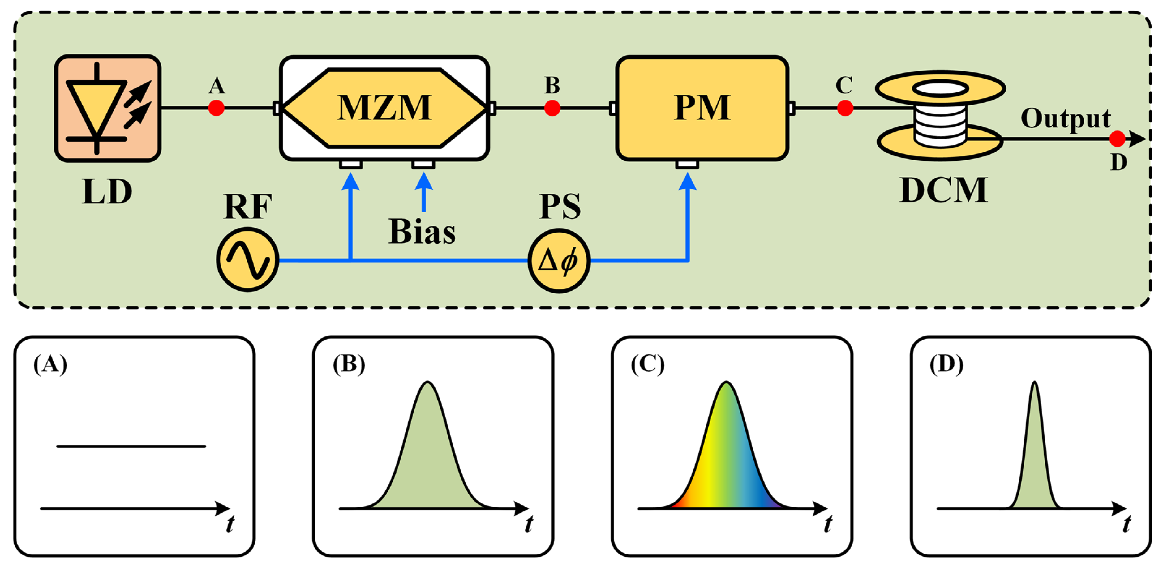
Figure 4 shows the architecture of the optical source. Continuous-wave (CW) light from a laser diode (LD) is first injected into an electro-optic MZM biased at its quadrature point and driven by a single-tone microwave signal with a peak-to-peak voltage equal to its half-wave voltage. Hence, an optical pulse train with a repetition frequency equal to the microwave signal is generated. Then, the optical pulse train is injected into an electro-optic phase modulator (PM) also driven by the single-tone microwave signal. Thereinto, the phase of the microwave signal is finely adjusted by using a phase shifter (PS) to guarantee that the peak or the valley of the microwave signal aligns with each optical pulse in the PM. In addition, the microwave signal applied to the PM is with a high power. On this condition, a large linear chirp is introduced into each optical pulse. Finally, the linear chirp of the optical pulse is compensated by using a dispersion compensation module (DCM). As a result, an ultra-short optical pulse train with a picosecond-level pulse width is generated, where the repetition frequency is equal to the single-tone microwave signal applied to the modulator.
In the simulation, the single-tone microwave signal used in the optical source is with a frequency of 20 GHz and a time jitter of 50 fs. The modulation indices of the MZM and the PM are set to 0.5π and 2π, respectively. Correspondingly, a DCM with a group velocity dispersion (GVD) value of 9.69 ps/nm is employed to compensate for the modulation-induced chirp.
Figure 5 shows the waveform of the generated high-speed uniform optical pulse train. The repetition frequency and the pulse width are 20 GHz and 2.65 ps, respectively.
The high-speed uniform optical pulse train with a repetition frequency of fδ = 20 GHz (i.e., δ = 50 ps) is divided into twenty groups of low-speed uniform optical pulse trains (i.e., M = 20), each of which is with a repetition frequency of fμ = 1 GHz (i.e., μ = 1 ns). Then, the twenty groups of low-speed uniform optical pulse trains are connected in sequence to form a low-speed non-uniform optical pulse train with an average repetition frequency of fμ = 1 GHz. The interval between the last sampling pulse in the previous group and the first sampling pulse in the next group is μ + δ = 1.05 ns. The sampling number of the NPS-based ADC is set to n = 2000, which corresponds to a spectral resolution of Δf = fδ/n = 10 MHz. Based on the proposed NPS strategy, an electro-optic MZM biased at its minimum point is driven by a PPG to specifically select the low-speed non-uniform sampling optical pulses from the high-speed uniform optical pulse train, while the other optical pulses are blocked.
In the part of photonic sampling, the low-speed non-uniform sampling optical pulse train is modulated by a single-tone signal with a frequency of 9.9 GHz via a broadband electro-optic MZM biased at its quadrature point, where the modulation index is set to be
π/8.
Figure 6a shows the waveform of the sampled optical pulse train. Then, a PD with a 3-dB bandwidth of 1 GHz is used to achieve photoelectric conversion of the sampled optical pulse train, where the unit impulse response time of the PD is shorter than the minimum sampling interval of 1 ns.
Figure 6b presents the waveform from the PD. It can be seen that, although the pulse width is broadened after photodetection, its profile is identical to that in
Figure 6a, indicating that the fidelity of the input signal is maintained. Subsequently, a T/H circuit with a 3-dB bandwidth of 1 GHz and synchronized with the low-speed non-uniform sampling optical pulse train is used to maintain the voltage level of each sample until the next sample arrives.
Figure 6c exhibits the waveform from the T/H circuit. Finally, an electronic ADC with a uniform sampling rate of 1 GSa/s, an operation bandwidth of 1 GHz and an effective number of bits (ENOB) of 7 bits is used to digitize the waveform from the T/H circuit. The electronic ADC is synchronized with the cavity-less ultra-short optical pulse source via a clock circuit, and its sampling clock is carefully tuned to guarantee that the uniform sampling instants of the electronic ADC fall in each duration of the nonuniform sampling period as depicted in
Figure 7. The appropriate position of the sampling instant is with a time interval of
δ, which can be adjusted by using a high-precision variable optical delay line with a delay precision of about tens of femtoseconds.
The data stream from the electronic ADC is sent to a desktop computer (Intel Core i7-9700 CPU @ 3 GHz) to achieve signal reconstruction based on the proposed algorithm.
Figure 8a shows the reconstructed spectrum of the input signal. It can be seen that the recovered signal is a single-tone microwave signal at 9.9 GHz, which is identical to the input signal. The relatively large spur at 9.7 GHz is attributed to the 3rd-order modulation nonlinearity of the MZM, i.e., 9.9 × 3 − 20 = 9.7 GHz. For comparison, the equivalent high-speed uniform photonic sampling with a sampling rate of 20 GSa/s is used to digitize the same input single-tone microwave signal. In order to facilitate comparison, the sampled optical pulse train is digitized by using a single electronic ADC with a sampling rate of 20 GSa/s, an operation bandwidth of 10 GHz and an ENOB of 7 bits.
Figure 8b presents the spectrum obtained by implementing FFT calculation. It can be seen from
Figure 8 that the reconstructed spectrum based on the proposed NPS is identical to that based on its equivalent high-speed uniform photonic sampling. The only difference lies in that the reconstructed signal power by using the NPS is 10 dB lower than that obtained by using its equivalent high-speed uniform photonic sampling. This is attributed to the ten times reduction in the operation bandwidth in the low-speed NPS. However, the noise floor is also reduced by 10 dB in the NPS. The ENOBs in
Figure 8a,b are calculated to be 6.43 bits and 6.35 bits, respectively, indicating the SNR is maintained in the NPS-based ADC.
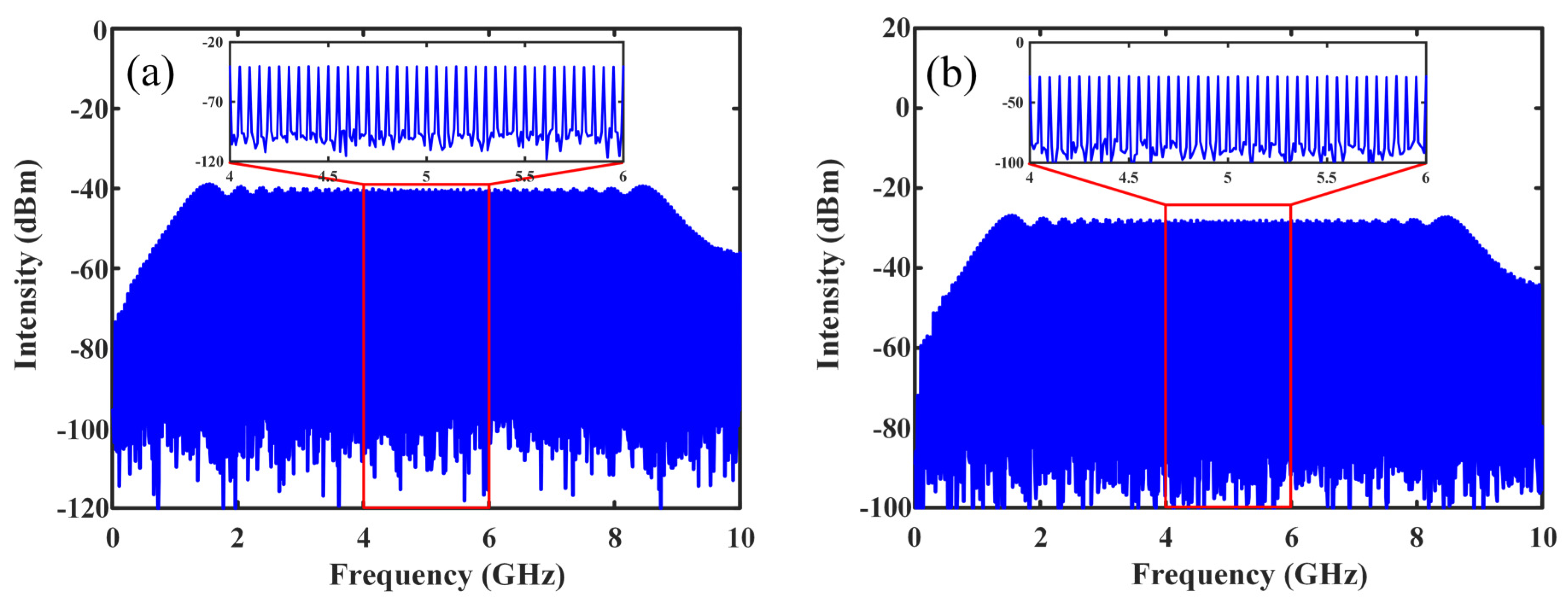
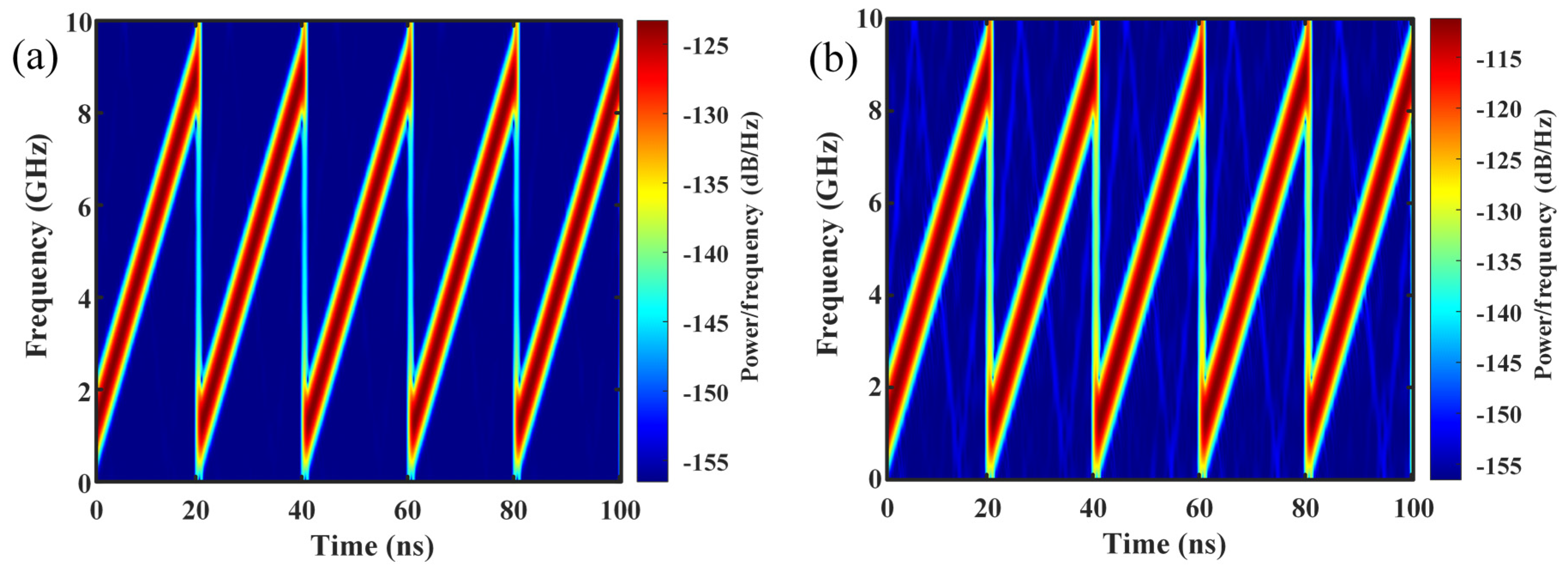
The low-speed NPS-based ADC can also be used to digitize a broadband signal. A periodic LFM signal in the frequency range of 1 GHz to 9 GHz and with a period of 20 ns is used as the input signal. The reconstructed spectrum and the time-frequency diagram obtained by using the NPS-based ADC are shown in
Figure 9a and
Figure 10a, respectively. For comparison, the LFM signal is also digitized by using the equivalent high-speed uniform photonic sampling with a sampling rate of 20 GSa/s. The spectrum obtained by implementing FFT calculation and the time-frequency diagram are exhibited in
Figure 9b and
Figure 10b, respectively. The results indicate that the two sampling schemes have an identical performance for digitizing a broadband signal. Although the sub-Nyquist sampling factor
M is equal to 20 in the simulation, it can be further enhanced if the duration of the periodic signal is large enough. The maximum sub-Nyquist sampling factor is equal to the ratio of the signal duration to the time window of the equivalent high-speed uniform sampling. In order to vary the sub-Nyquist sampling factor, the sampling period of each group of the low-speed uniform sampling (i.e.,
μ) need to be changed via the PPG, and the sampling rate of the T/H circuit and electronic ADC should be set to match with the low-speed uniform sampling rate (i.e., 1/
μ).
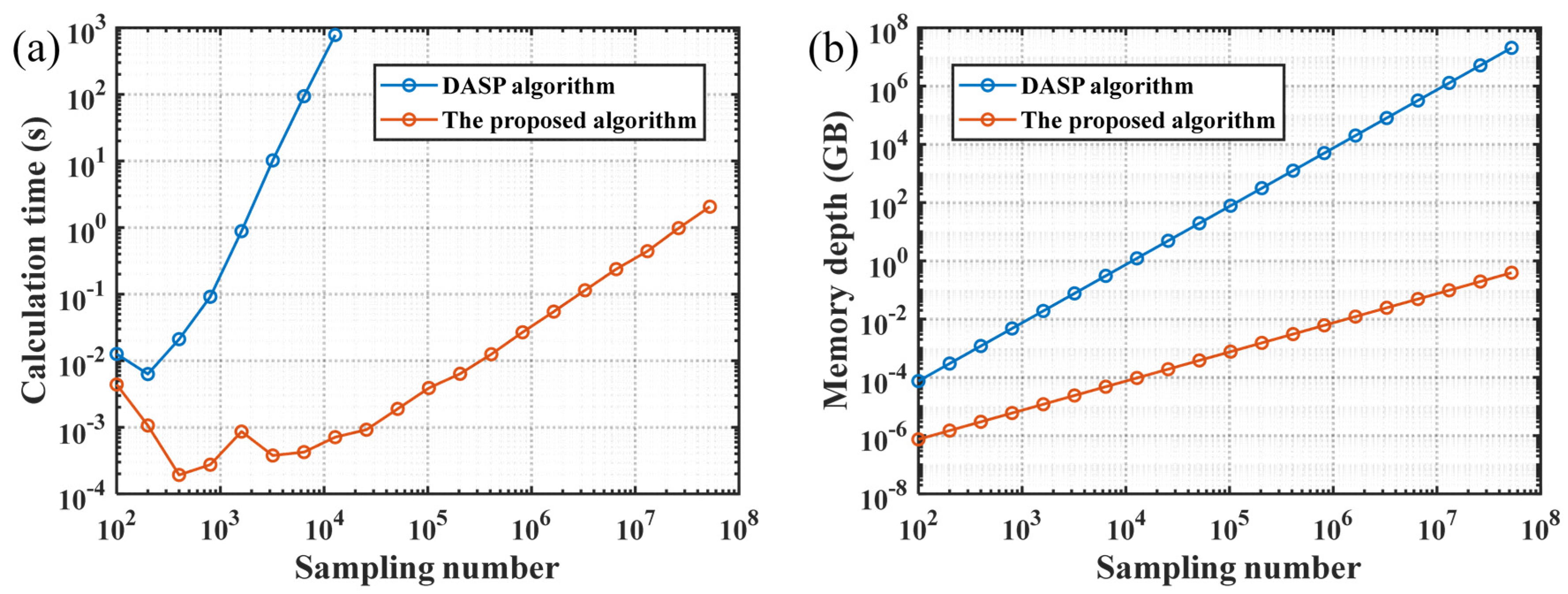
Figure 11a shows the calculation time of the proposed signal reconstruction algorithm and the DASP algorithm in [
21] under different sampling numbers. When the sampling number is greater than 10
4, the calculation time of the proposed algorithm is millions of times lower than that of the DASP algorithm, which is benefited from the FFT calculation of a one-dimensional data array in the proposed algorithm instead of the two-dimensional data array calculation in the DASP algorithm. In addition, when the sampling number exceeds 10
5, the memory depth used to store the fitting matrix in the DASP algorithm is more than 78 GB. As a comparison, the memory depth used in the proposed algorithm is equal to the sampling number, which is much smaller than that in the DASP algorithm, as depicted in
Figure 11b.
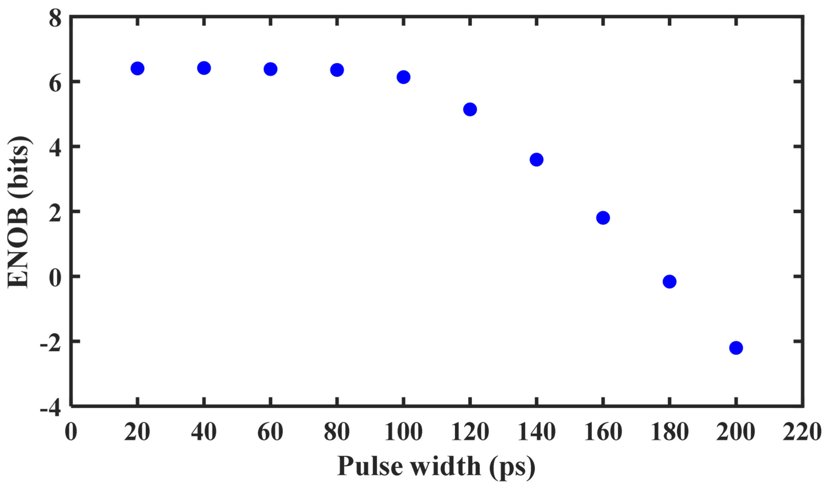
In fact, although the NPS effectively decreases the bandwidth requirement of the back-end electronic devices, a high-speed PPG is indispensable to assist in generating the low-average-speed non-uniform optical pulse train from a high-speed uniform optical pulse train. Due to the limited bandwidth and speed of the PPG, the pulse width of the electrical pulse from the PPG may not be narrow enough to assist in selecting a single optical pulse at a time. Hence, residuary optical pulses may be generated on both sides of the selected optical pulse, as shown in
Figure 12, which will deteriorate the performance of the NPS-based ADC.
Figure 13 shows the ENOBs of the NPS-based ADC under different pulse widths from the PPG, where the electrical pulse generated by the PPG is supposed to be with a Gaussian shape, and the equivalent high-speed uniform photonic sampling rate is 20 GSa/s. It can be seen from
Figure 13 that the performance of the NPS-based ADC is immune to the residuary optical pulses when the pulse width of the electrical Gaussian pulse from the PPG is smaller than 80 ps. This result indicates that the NPS-based ADC has a high tolerance for the rising/falling time of the PPG and the extinction ratio of the MZM used to select the low-average-speed non-uniform optical pulse train.
Finally, it should be pointed out that the NPS-based ADC is only applicable for the case that the time window of the equivalent high-speed uniform sampling (i.e., time window of the Fourier analysis) is equal to an integral multiple of the input signal period, which is to avoid the spectrum leakage. Therefore, it is not suitable for the application scenarios in which the signal is aperiodic, or the period of the signal is unknown. In the radar system, the repetition frequency of the transmitting signal must be set to be a fractional integer of the equivalent high-speed uniform photonic sampling rate. In the electronic reconnaissance system, the period of the enemy radar signal must be measured in advance. Then, the repetition frequency of the high-speed uniform optical pulse train from the ultra-short optical pulse source should be tuned to accommodate to the receiving signal. Fortunately, free tuning of the repetition frequency can be achieved by using the cavity-less ultra-short optical pulse source in
Figure 4. Furthermore, the proposed non-uniform sampling strategy and the corresponding signal reconstruction algorithm may have potential applications in optical imaging, such as optical coherence tomography (OCT) [
26,
27].


