Abstract
Storage capacity of a conventional optical disc can be enhanced significantly by recording data within the three-dimensional volume. However, spherical aberrations and light-scattering limit the number of layers that can be efficiently recorded and retrieved. In this paper, we show that by optimizing the multi-layer data recording and reading parameters, the number of fabricated layers could be tripled to 60 in commercial grade poly-methyl-methacrylate polycarbonate and reduce the read laser power by a factor of 7 by the 20th layer. Influence of spherical aberration on write laser spot size was studied by using vector diffraction theory and compared with experimental values obtained by monitoring the threshold energy of the write laser with depth. Scattering losses of the read laser were studied by simulating the propagation of light through multi-layered micro-structured material. The main advantage of our technique is its practical implementation, as it refrains from the use of index-matching liquids and specialized optics during the read–write process.
1. Introduction
The majority of the data generated globally every year is the so-called cold data that needs long-term storage for archival purposes and is accessed only occasionally. Consequently, there is an ever-increasing demand for not only higher data storage capacities but also longer shelf life. Among the existing technologies, optical data storage (ODS) has a better shelf life but lags behind magnetic and silicon-based technologies in terms of data storage capacity. This is because in conventional optical discs (DVDs and Blu–ray), data is stored on the surface, and this planar technology cannot be scaled due to the response and design of materials below 400 nm. This limitation can be overcome by encoding multilevel and multiplexed information within the three-dimensional volume of a recording medium.
The 3D ODS often relies on using ultra-fast lasers to induce permanent changes in the medium on a micron scale in the form of refractive index/birefringence [1,2], aggregation/shape alteration of metal nanoclusters/rods [3,4], or emission centers [5]. It was first demonstrated in photopolymers [6] and glass [2] by modifying the refractive index to record data bit by bit. The technique was later extended to demonstrate 4D ODS in silver-doped zinc phosphate glass in which the write laser-induced silver nanoclusters that emitted fluorescence, upon excitation by the read laser, whose intensity represented the fourth dimension [3]. The 5D ODS was recently demonstrated in glass by using laser-induced form birefringence and in stacked gold nanorods mediated by surface plasmon resonances [4,7,8]. In addition to three spatial dimensions, the former exploited two additional dimensions associated with the orientation and retardance of periodic nanostructures, whereas the latter exploited wavelength and polarization of light to multiplex data within the same bit. Recent advances to significantly enhance the storage capacity, in principle, include employing techniques such as multifocal optical nanoscopy [9]. Stimulated emission depletion in specially designed photoresists [10], development of nanocomposites [11], and incorporation of machine learning algorithms [12]. However, their implementation in developing a viable consumer electronic device remains challenging.
Data recorded in a pristine transparent medium with ultra-fast lasers is not erasable and therefore not rewritable. Such ODS, categorized as write once read many times (WORM) type, ensures the highest level of data security and integrity with applications in archival storage. Erasable/rewritable 3D ODS systems require photo-refractive polymers [13] or transparent glasses doped with rare-earth ions [14] or nanocrystals [15]. Alternate technologies, such as holography and two-beam lithography, do not rely on ultra-fast lasers to record bits but require a specially designed photosensitive recording medium [16,17].
The capacity of an ODS is determined by the bit size and spacing, and the number of layers embedded in the recording medium. Smaller bit sizes can be achieved by using a higher numerical aperture (NA) objective in conjunction with index-matching liquids. However, their usage in a practical implementation is restrictive, especially when existing Blu-ray/DVD technology is extended to 3D ODS. Moreover, spherical aberrations and light-scattering generally limit the number of layers that can be efficiently recorded and retrieved. This is true even for the practical and cost-effective 4D ODS technology that we demonstrated in readily available common plastics based on fluorescence emission from femtosecond laser-modified regions [5].
In ODS, the beam emerging from the high-NA objective focuses deeply through an interface between two media of different refractive index leading to spherical aberrations, which increases dynamically at increasing depths. Consequently, the spot size of the write laser increases with depth leading to an increase in the threshold fluence required to record a bit. Spherical aberrations can be compensated by correcting the wavefront by using passive or adaptive optics (such as a spatial light modulator or digital micro-mirror device) to dynamically adjust for different depths [18,19]. Because the practical implementation of such correction techniques is not easy, we adopted a simpler technique of varying the pulse energy with depth during the recording process.
In this letter, we maximize storage capacity without the use of index-matching liquids and employing an energy gradient technique to compensate spherical aberrations of the write laser beam. We optimize the coupling of read laser light by simulating the propagation of light through multi-layered micro-structured material. We effectively tripled the number of layers that can be fabricated in a commercial grade PMMA and also reduced the read laser power requirement by a factor of 7. We measured the threshold fluence required to record bits at different depths to extract the aberrated spot sizes. The write laser power was then accordingly adjusted for each layer to maintain the same fluence while recording the bits. We used vector-diffraction theory to simulate the variation of spot size with depth and compared it with the measured values. To maintain a constant readout signal, we show that the read laser power needs to be adjusted layer to layer to account for scattering losses during propagation through multi-layered nanostructures.
2. Methods
2.1. Data Fabrication
Femtosecond pulses from a Ti:sapphire laser system (800 nm, 1 kHz, 45 fs, 2.5 mJ/pulse) were focused inside clinical quality (CQ grade from Goodfellow, UK), commercial grade (CG) PMMA samples and commercial grade polycarbonate (PC) with a 0.5, 0.83 numerical aperture (NA) aspheric objective. Samples with the thickness of 2 mm were mounted on three-axis translation stages with a resolution of 100 nm (Figure 1a). Pulse energies, measured after the aspheric objective, were varied from ≈ 25–70 nJ by a combination of half-wave plate and polarizer. The pulse duration at the aspheric objective was 70 fs, monitored continuously by using a single-shot auto-correlator. Multiple layers were fabricated in PMMA starting from the bottom with the last layer being at 100 µm depth from the top surface. Each layer consisted of a 25 × 25 array of bits/modified regions, each irradiated with a single laser pulse. Typical bit spacing was 2.0, 0.8 µm, and the layer spacing was 10 µm. Fluorescence emission from bits was recorded by using a Nikon confocal fluorescence microscope with a 40x objective (NA 0.8/1.1, working distance 2 mm, water immersion) at an excitation wavelength of 488 nm, and an emission window in the 500–550 nm range, respectively. Sensitivity of the detector at 488 nm excitation was 140 and the pinhole size for confocal microscope was optimized at 39.6 µm. The CW read laser power measured at the sample was in the range of 1 µW–150 µW.
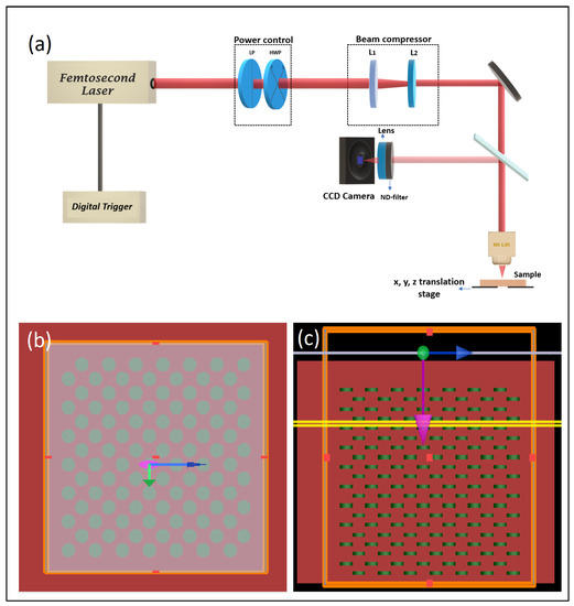
Figure 1.
(a) Schematic (b,c) Top and side view of the FDTD grid showing the layout of the modeled nanostructured PMMA. The pink arrow shows the plane wave propagation direction. In addition, the blue (green) arrow represents electric (magnetic) field. Yellow lines, positioned 1 µm above and below each layer, represent the power and field profile monitors.
2.2. Aberration Correction by Energy Gradient
Spherical aberrations increase the laser spot size with depth. Consequently, the threshold energy to induce modification in a medium increases. If the incident pulse energy is not dynamically adjusted with depth to compensate for the change in laser fluence, the number of layers that can be fabricated is limited. This can be overcome by adjusting the incident pulse energy to the threshold value, which ensures a minimum laser spot size and spherical aberration. To determine the variation of threshold pulse energies with depth, a single layer containing an array of bits was fabricated at different depths with an incremental increase in pulse energy between adjacent lines within the array. This information was implemented during the automated fabrication of data in different layers.
2.3. Numerical Simulations
2.3.1. Spherical Aberrations
The effect of aberrations on the spot size was quantified by using the vector diffraction theory developed by Wolf [20] and Torok [21,22]. The focusing lens was assumed to be free of spherical aberration and the wavefront was assumed to be uniform at the focusing plane. The Cartesian components of the electric field at any point p inside the material of refractive index n2, is given by a linear combination of diffraction integrals:
where
and
Here, and are angles of incidence and refraction at the interface between two materials of mismatched refractive indices and the aberration function
and the normalized radial and axial coordinates v and u are given by , , where is the solid semi-angle of the lens in the first material, , and are the wave numbers in the vacuum, first and second medium (PMMA), respectively, f is the focal length of the lens in the vacuum, is an electric field amplitude factor, , and and are spherical polar coordinates to the point p where the fields are being evaluated. The standard expressions were used for the Fresnel transmission coefficients and and for the Bessel functions of the first kind. Numerical integration was performed by using the adaptive Gauss-quadrature method and evaluated at the first maximum of energy density in z.
2.3.2. FDTD Simulation
To optimize the coupling of the read laser light, we simulated the absorption of the plane wave (478–498 nm) traversing through 20 layers of laser-modified regions/bits in PMMA by using the FDTD: 3D Electromagnetic Simulator (Lumerical FDTD Solutions, Inc., Vancouver, Canada) Each laser-modified region/bit was assumed to have a cylindrical structure (1 µm diameter and 4 µm length) with 0.15% higher refractive index than the surrounding, unmodified PMMA and an imaginary refractive index of about 8 × 10 [23]. A 7 × 7 array with a bit spacing of 2 µm was considered with periodic boundary conditions in the transverse x–y plane. The first layer was positioned 30 µm below the surface and subsequent layers were spaced 10 µm apart. Total simulation dimensions were 15 × 15 µm in the transverse plane and 230 µm along the propagation direction. Power and field profile monitors were positioned 1 µm above and below each layer to study the propagation of light. The side and top view of the FDTD simulation model is shown in Figure 1b,c.
3. Results
Figure 2 shows the variation of fluorescence intensity of an array of bits from different layers fabricated in CQ and CG grade PMMA for different bit spacing (Figure 2a) and layer spacing (Figure 2b). Bits in each layer were fabricated with fixed incident energy. Fluorescence intensity drops significantly as the number of layers increases. Vertical dashed lines represent the layers where the read laser power had to be increased and the fluorescence intensity normalized. CG-PMMA produces a lesser fluorescence signal compared to CQ-PMMA. As a result, only 21 layers could be fabricated in CG-PMMA compared to 35 in CQ-PMMA. This is most likely due to the different chemical compositions of the additives and UV stabilizers. For a fixed layer spacing of 10 µm, the fluorescence signal is lower for smaller bit spacing (Figure 2a). Confocal images of layers 5, 15, 25, and 35 are shown in Figure 2c, d, e, and f respectively, for a bit spacing of 2.0 µm.
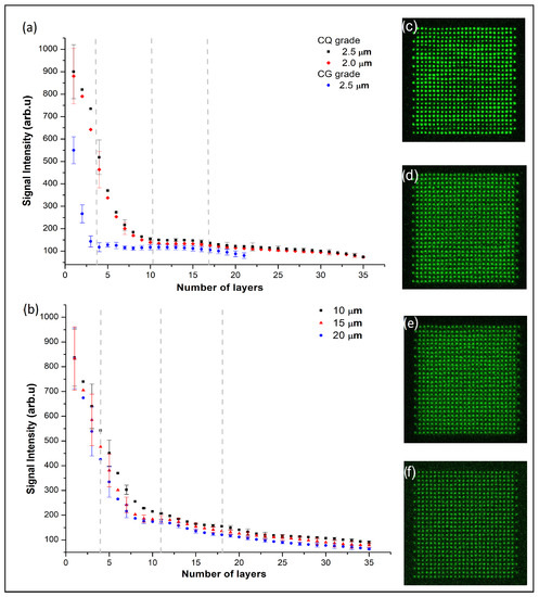
Figure 2.
Variation of fluorescence intensity with the number of layers fabricated in PMMA for (a) fixed layer spacing of 10 µm and bit spacing of 2.0, 2.5 µm in clinical quality (CQ), and 2.0 µm in commercial grade (CG), and (b) fixed bit spacing of 2.0 µm and layer spacing of 10, 15, and 20 µm in CQ grade. Vertical dashed lines represent the layers where the read laser power was adjusted to produce the same fluorescence signal (see text for details). (c–f) Confocal microscope images of bit arrays, fabricated at a fixed energy of 35 ± 3 nJ energy, for layers 5, 15, 25, and 35, respectively.
There are two major contributions to the rapid change in fluorescence intensity with the number of layers: (1) spherical aberrations influencing the write laser fluence, and (2) coupling losses of the read laser due to scattering from multiple micro-structured layers. For a fixed bit spacing (Figure 2b), the former leads to lower fluorescence intensity with the increase in layer spacing. This is because the depth at which the layers are fabricated increases, causing the spherical aberration to increase the laser spot size and thereby reduce the fluence for a fixed incident pulse energy. The latter requires the use of higher read laser powers. With a 0.5 NA aspheric objective, 10 µm is the optimum layer spacing—a balance between aberrations (that scales with NA of the objective) and cross-talk between layers (that depends on the confocal parameter).
The influence of spherical aberrations on the ability of the write laser to fabricate bits at different depths is shown in Figure 3. For this study, a single layer containing an array of bits was fabricated at different depths with an incremental increase in pulse energy between adjacent lines within the array. As the depth increased the number of lines in the array visible under an optical microscope decreased, as shown in Figure 3b–d. This is due to an increase in the threshold fluence required to modify PMMA as a result of an increase in the spot size from spherical aberrations. Figure 3a shows the threshold energy required to observe fluorescence from bits at different depths. A nearly linear variation of write laser energy with depth makes it easy to implement an energy gradient during the automated fabrication of data in different layers.
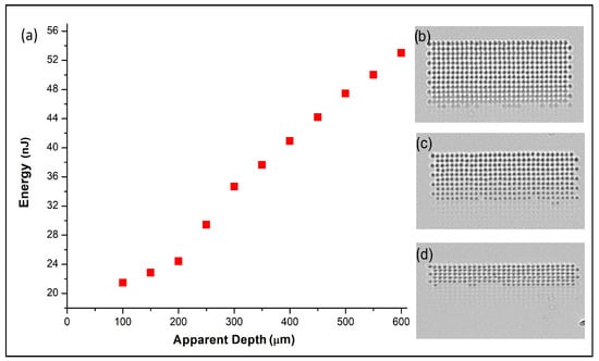
Figure 3.
(a) Variation of threshold energy required to fabricate bits at different depths in PMMA. (b–d) Optical microscope images of an array of bits, fabricated with increasing pulse energies from bottom to top, at depths of 100, 150, and 350 µm.
Figure 4 shows the variation of write laser spot size, both experimental and simulated, with depth inside PMMA. Experimentally, the spot size was extracted from Figure 3 by comparing the threshold fluorescence intensity for a given layer with that of the first layer (100 µm below the surface) as a reference. The spot size was obtained by considering bits at different depths (50 µm apart) fabricated with a specific write laser energy that produced fluorescence intensity similar to the reference signal. The effect of aberrations on the spot size was quantified by using the vector diffraction theory developed by Wolf [20] and Torok [21,22] (see Methods).
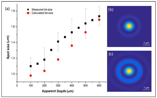
Figure 4.
(a) Variation of spot size with depth in PMMA extracted from the threshold energies of Figure 3 (black squares) and calculated from the vector diffraction theory (red circles). (b,c) Spatial profile of the simulated laser spot size at depths of 100 µm and 200 µm focused inside PMMA with a 0.5 NA aspheric objective.
The spatial profile of the simulated focal spot produced by a 0.5 NA aspheric objective at an apparent depth of 100 and 200 µm inside the PMMA is shown in Figure 4b,c. Spherical aberration increases the spot size and energy density in the secondary maxima of the Airy pattern with depth. Simulated bit sizes were obtained by taking 1/e diameter of the central maxima in the diffraction pattern. Agreement with the experimentally obtained spot sizes establishes the fact that non-linear effects such as self-focusing are not dominant at the write laser energies used (up to 60 nJ).
In commercial grade PMMA employing fixed write laser energy, the maximum number of layers that could be recorded and retrieved is limited to only 20 layers, beyond which fluorescence intensity is comparable to background noise (Figure 2a). By employing the energy gradient technique to offset spherical aberration effects and shifting alternate layers in the x–y direction by half the bit spacing, we could fabricate 60 layers with 10 µm layer separation and 2 µm bit spacing in each 25 × 25 array as shown in Figure 5a. Multiple layers were fabricated by incrementally increasing the write laser energy based on the dependence of threshold energy on depth (Figure 3a). Figure 5b shows the dependence of read laser power required to record different layers for the two fabrication methods—fixed write laser energy and energy gradient. For the latter, the read laser power is lower by a factor of 7 for the 20th layer. Lower read laser powers ensure no photo-bleaching of the emission centers induced by the write laser, hence no damage to the recording medium.
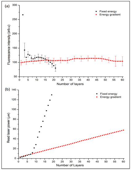
Figure 5.
Fabrication of 60 layers in commercial grade PMMA by compensation of spherical aberrations. Fluorescence intensity variation (a), and read laser power variation (b) as a function of the number of layers fabricated with fixed pulse energy (black squares) and with energy gradient technique (red circles).
The effectiveness of our method is demonstrated by fabricating 50 layers of data with 0.9 µm bit spacing and 10 µm layer spacing in CG grade PC (Figure 6a–c) by using a 0.8 NA objective with no index-matching liquid. The NA of the objective is similar to the one used in Blu-ray disc making it a viable 3D ODS technology. Spherical aberrations are more dominant when using such a higher NA objective. However, our method is effective in minimizing spherical aberrations with higher NA objectives up to depths of ∼400 µm where the bit size increased only by ∼25% (Figure 6f). The read laser power required to obtain nearly constant fluorescence intensity from different layers is shown in Figure 6d,e.
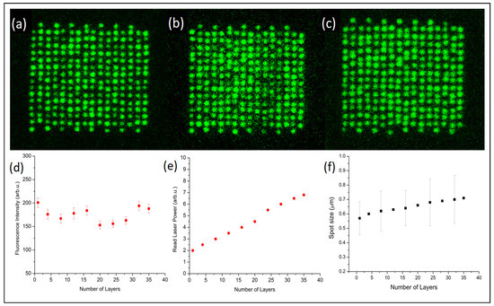
Figure 6.
Fabrication of 35 layers in commercial grade PC using a 0.83NA lens. (a–c) Confocal microscope images of bit arrays with 0.9 µm bit-spacing, for layers 8, 16, and 35, respectively. Fluorescence intensity variation (d), and read laser power variation (e) as a function of number of layers fabricated with energy gradient technique (red circles), (f) Spot size variation as a function of number of layers.
The gradual increase in the read laser power with depth is due to coupling losses arising from scattering and absorption from micro-structured multiple layers. To optimize the coupling of the read laser light, we simulated the absorption of a plane wave (478–498 nm) traversing through 20 layers of laser modified regions/bits in PMMA by using the FDTD: 3D Electromagnetic Simulator (Lumerical FDTD Solutions, Inc., see Methods).
Figure 7a–f shows the field patterns 1 µm below layers 8, 9, and 10, respectively, for two cases in which the bits in alternate layers are either unshifted and lie on top of each other (top row) or shifted in the x–y direction by 1 µm (middle row). In the unshifted case, after propagating through the first few layers, the scattered light localizes near the bits and in the regions between the bits. As the number of layers increases, the scattered light in the regions between the bits increases in magnitude (Figure 7a–c) and less light propagates in the center relative to the edges. Consequently, during imaging, this can reduce the contrast between bits and lead to darkening of the central region of an array of bits as observed previously [24]. When bits are shifted between alternate layers, light is localized near the bits with very little scattering in the surrounding regions (Figure 7d–f). As a result, the bit contrast is enhanced, and coupling losses are reduced.
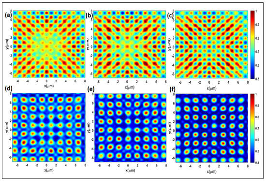
Figure 7.
Simulated field patterns of light propagating through an array of unshifted bits between alternate layers, (a–c) 1 µm below layers 8, 9, and 10, respectively. (d–f) The same as above for the shifted bits.
Figure 8a,b shows field patterns 1 µm above layer 9 for the unshifted and shifted bits cases, respectively. In the unshifted case, field patterns change drastically while propagating a distance of less than 5 µm. The regions where fields are stronger, just after layer 8 (Figure 7a), become weaker and vice versa. However, in shifted case, light undergoes a simple defocusing effect.
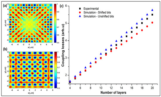
Figure 8.
Simulated field patterns of light propagating through an array of unshifted bits between alternate layers, (a) 1 µm above layer 9. (b) The same in case of the shifted bits. (c) Experimental (black) and simulated read laser coupling losses for unshifted (blue) and shifted bits (red).
Figure 8c shows the simulated coupling losses of the read laser for shifted (red) and unshifted bits (blue). Relative losses are low for the layers close to the top surface but increase significantly with the number of layers. Assuming coupling losses to be the major contributor for an increase in read laser power, we compare the simulated losses directly with the experimental variation of the read laser power as shown (black). Fabrication and imaging of 60 layers shown in Figure 5 were only feasible by shifting the bits between alternate layers. For the unshifted case, the maximum number of layers that could be imaged was about 25.
4. Discussion and Conclusions
Development of 3D ODS technology with enhanced storage capacity relies on simultaneous innovations in two research areas. First, we must find a suitable recording medium capable of storing data in multiple layers with a long shelf life. Secondly, we must spatially localize the data bits and retrieve them from multiple layers.
By using common, inexpensive transparent plastics such as PMMA and PC, we eliminate the need to search for and develop novel composite materials that exhibit photosensitive properties. The embedded data is thermally stable up to the glass transition temperature of the recording medium, thereby offering a long shelf life [5]. PMMA and PC do not fluoresce inherently. Irradiation by an ultra-fast laser results in the localized formation of carbonaceous clusters [25,26] within the focal volume that fluoresces upon excitation. In other words, the ultra-fast laser induces photo-sensitivity.
By refraining from the use of index matching liquids and specialized optics during the read–write process, we demonstrate enhanced storage capacity. This was achieved by minimizing spherical aberrations during the write process and optimizing the light-scattering during the read process. Our method enables practical implementation in developing a viable consumer electronic device. Higher bit density can be achieved with high NA objectives but requires index-matching liquids and is limited by the working distance of the objective. Our method does not use index-matching liquids to compensate for spherical aberrations but exploits the depth variation of threshold pulse energies required for modification. However, it requires an accurate determination of the threshold pulse energies. Any variations in incident pulse energy or determining the threshold energies can lead to either darkening of bottom layers or a low signal-to-noise ratio. In addition, for objectives greater than 1 NA, the method can be ineffective in minimizing aberrations beyond 60 layers (120 layers bi-directional). To simulate spherical aberrations, the focusing lens was assumed to be aberration-free and the wavefront was assumed to be uniform at the focusing plane.
To optimize the coupling of the read laser with different layers in a stack and the scattering of fluorescence signal from the above layers, FDTD simulations assumed each laser-modified region/bit to have a cylindrical structure to mimic the experimental Rayleigh range. Varying the radial bit size changes the scattering regime from Rayleigh to Mie scattering. As a result, the contrast between the modified and unmodified regions is higher when the bit size is greater than the wavelength of the read laser and reduces when the bit size is smaller than the wavelength of light. Varying the axial bit length influences the cross-talk between the adjacent layers and determines the number of layers that can be packed in a standard optical disc. Light coupling is also influenced by the bit spacing. There is an optimum bit spacing that allows a maximum number of layers that can be detected. According to FDTD simulations, a bit spacing of minimum of 1.5 gives the best contrast and enables the reading of maximum number of layers.
To conclude, we demonstrate the fabrication and imaging of 60 layers of data in CG grade plastics by optimizing the multi-layer data recording and reading parameters. This allows us to stack 120 layers of data in a standard 1.2-mm-thick optical disc by using bidirectional read–write geometry. Optimization using our technique highlights the practical implementation of our method into a fluorescence-based optical data storage technology. A storage capacity of 275-GB disc can be easily realized with the demonstrated bit spacing of 0.9 µm. This can be further enhanced by reducing the bit size (and therefore bit spacing) by using higher NA lenses and shorter wavelengths. Employing adaptive aberration correction and reduced axial bit dimension can potentially lead to recording 150 layers of data in PMMA. Manipulating light propagation by strategically introducing gaps between a set of layers in order for the light to regroup, can further reduce coupling losses of the read laser.
Author Contributions
A.J., M.G.R. and V.R.B. designed and planned the experiments. A.J. and M.G.R. conducted the experiments and analyzed the results. A.J. conducted theoretical simulations. All authors have read and agreed to the published version of the manuscript.
Funding
The authors acknowledge financial support from the Natural Science and Engineering Research Council of Canada, Canadian Foundation for Innovation.
Institutional Review Board Statement
Not applicable.
Informed Consent Statement
Not applicable.
Data Availability Statement
The data that support the findings of this study are available from the corresponding author on request.
Conflicts of Interest
The authors declare no conflict of interest.
Abbreviations
The following abbreviations are used in this manuscript:
| PMMA | Poly-methyl-methacrylate |
| PC | Polycarbonate |
| ODS | Optical data storage |
| NA | Numerical aperture |
| CQ | Clinical quality |
| CG | Commercial grade |
References
- Glezer, E.N.; Milosavljevic, M.; Huang, L.; Finlay, R.; Her, T.; Callan, J.; Mazur, E. Three-dimensional optical storage inside transparent materials. Opt. Lett. 1996, 21, 2023–2025. [Google Scholar] [CrossRef] [PubMed]
- Zhang, J.; Gecevičius, M.; Beresna, M.; Kazansky, P. Seemingly Unlimited Lifetime Data Storage in Nanostructured Glass. Phys. Rev. Lett. 2014, 112, 033901. [Google Scholar] [CrossRef]
- Royon, A.; Bourhis, K.; Bellec, M.; Papon, G.; Bousquet, B.; Deshayes, Y.; Cardinal, T.; Canioni, L. Silver Clusters Embedded in Glass as a Perennial High Capacity Optical Recording Medium. Adv. Mater. 2010, 22, 5282–5286. [Google Scholar] [CrossRef] [PubMed]
- Zijlstra, P.; Chon, J.; Gu, M. Five-dimensional optical recording mediated by surface plasmons in gold nanorods. Nature 2009, 459, 410–413. [Google Scholar] [CrossRef] [PubMed]
- Kallepalli, D.; Alshehri, A.; Marquez, D.; Andrzejewski, L.; Scaiano, J.; Bhardwaj, R. Ultra-high density optical data storage in common transparent plastics. Sci. Rep. 2016, 25, 26163. [Google Scholar] [CrossRef] [PubMed]
- Strickler, J.; Watt Webb, W. Three-dimensional optical data storage in refractive media by two-photon point excitation. Opt. Lett. 1991, 16, 1780–1782. [Google Scholar] [CrossRef]
- Shimotsuma, Y.; Sakakura, M.; Kazansky, P.; Beresna, M.; Qiu, J.; Miura, K.; Hirao, K. Ultrafast Manipulation of Self-Assembled Form Birefringence in Glass. Adv. Mater. 2010, 22, 4039–4043. [Google Scholar] [CrossRef]
- Gu, M.; Li, X.; Cao, Y. Optical storage arrays: A perspective for future big data storage. Light. Sci. Appl. 2014, 5, e177. [Google Scholar] [CrossRef]
- Li, X.; Cao, Y.; Tian, N.; Fu, L.; Gu, M. Multifocal optical nanoscopy for big data recording at 30 TB capacity and gigabits/second data rate. Optica 2015, 2, 567–570. [Google Scholar] [CrossRef]
- Gan, Z.; Cao, Y.; Evans, R.A.; Gu, M. Three-dimensional deep sub-diffraction optical beam lithography with 9nm feature size. Nat. Commun. 2013, 4, 2061. [Google Scholar] [CrossRef]
- Lamon, S.; Wu, Y.; Zhang, Q.; Liu, X.; Gu, M. Nanoscale optical writing through upconversion resonance energy transfer. Sci. Adv. 2021, 7, eabe2209. [Google Scholar] [CrossRef] [PubMed]
- Lamon, S.; Zhang, Q.; Gu, M. Nanophotonics-enabled optical data storage in the age of machine learning. APL Photonics 2021, 6, 110902. [Google Scholar] [CrossRef]
- Day, D.; Gu, M.; Smallridge, A. Use of two-photon excitation for erasable–rewritable three-dimensional bit optical data storage in a photorefractive polymer. APL Opt. Lett. 1999, 24, 948–950. [Google Scholar] [CrossRef]
- Hu, Z.; Huang, X.; Yang, Z.; Qiu, J.; Song, Z.; Zhang, J.; Dong, G. Reversible 3D optical data storage and information encryption in photo-modulated transparent glass medium. Light Sci. Appl. 2021, 10, 140. [Google Scholar] [CrossRef]
- Lin, S.; Lin, H.; Ma, C.; Cheng, Y.; Ye, S.; Lin, F.; Wang, Y. High-security-level multi-dimensional optical storage medium: Nanostructured glass embedded with LiGa5O8: Mn2+ with photostimulated luminescence. Light Sci. App. 2020, 9, 22. [Google Scholar] [CrossRef] [PubMed]
- Ashley, J.; Bernal, M.; Burr, G.; Coufal, H.; Guenther, H.; Hoffnagle, J.; Jefferson, C.; Marcus, B.; Macfarlane, R.; Shelby, R.; et al. Holographic data storage technology. IBM J. Res. Dev. 2000, 14, 341–368. [Google Scholar] [CrossRef]
- Li, X.; Ren, H.; Chen, X.; Liu, J.; Li, C.; Xue, G.; Jia, J.; Cao, L.; Sahu, A.; Hu, B.; et al. Athermally photoreduced graphene oxides for three-dimensional holographic images. Nat. Commun. 2015, 6, 6984. [Google Scholar] [CrossRef]
- Simmonds, R.; Salter, P.; Jesacher, A.; Booth, M. Three dimensional laser microfabrication in diamond using a dual adaptive optics system. Opt. Express 2011, 19, 24122–24128. [Google Scholar] [CrossRef]
- Kontenis, G.; Gailevičius, D.; Jonušauskas, L.; Purlys, V. Dynamic aberration correction via spatial light modulator (SLM) for femtosecond direct laser writing: Towards spherical voxels. Opt. Express 2020, 28, 27850–27864. [Google Scholar] [CrossRef]
- Wolf, E. Electromagnetic diffraction in optical systems-I. An integral representation of the image field. Proc. R. Soc. Lond. A 1959, 253, 349–357. [Google Scholar]
- Török, P.; Varga, P.; Laczik, Z.; Booker, G. Electromagnetic diffraction of light focused through a planar interface between materials of mismatched refractive indices: An integral representation. J. Opt. Soc. Am. A 1995, 12, 325–332. [Google Scholar] [CrossRef]
- Török, P.; Varga, P.; Booker, G. Electromagnetic diffraction of light focused through a planar interface between materials of mismatched refractive indices: Structure of the electromagnetic field. I. J. Opt. Soc. Am. A 1995, 12, 2136–2144. [Google Scholar] [CrossRef]
- Baum, B.; Scully, P.; Basanta, M.; Thomas, P.; Fielden, P.; Goddard, N.; Perrie, W.; Chalker, P. Photochemistry of refractive index structures in polymethyl methacrylate by femtosecond laser irradiation. Opt. Lett. 2007, 32, 190–192. [Google Scholar] [CrossRef] [PubMed]
- Gao, L.; Zhang, Q.; Evans, R.; Gu, M. 4D Ultra-High-Density Long Data Storage Supported by a Solid-State Optically Active Polymeric Material with High Thermal Stability. Adv. Opt. Mater. 2021, 9, 2100487. [Google Scholar] [CrossRef]
- Alshehri, A.M.; Deepak, K.L.N.; Marquez, D.T.; Desgreniers, S.; Bhardwaj, V.R. Localized nanoclusters formation in PDMS upon the irradiation with femtosecond laser. Opt. Mater. Express 2015, 5, 858–869. [Google Scholar] [CrossRef]
- Nie, Z.; Lee, H.; Yoo, H.; Lee, Y.; Kim, Y.; Lim, K.S.; Lee, M. Multilayered optical bit memory with a high signal-to-noise ratio in fluorescent polymethylmethacrylate. Appl. Phys. Lett. 2009, 94, 111912. [Google Scholar] [CrossRef]
Publisher’s Note: MDPI stays neutral with regard to jurisdictional claims in published maps and institutional affiliations. |
© 2022 by the authors. Licensee MDPI, Basel, Switzerland. This article is an open access article distributed under the terms and conditions of the Creative Commons Attribution (CC BY) license (https://creativecommons.org/licenses/by/4.0/).