Abstract
It is challenging to realize the complete broadband absorption of near-infrared in thin optical devices. In this paper, we studied high light absorption in two devices: a stack of Au-pattern/insulator/Au-film and a stack of Au-pattern/weakly-absorbing-material/Au-film where the Au-pattern was structured in graded photonic super-crystal. We observed multiple-band absorption, including one near 1500 nm, in a stack of Au-pattern/spacer/Au-film. The multiple-band absorption is due to the gap surface plasmon polariton when the spacer thickness is less than 30 nm. Broadband absorption appears in the near-infrared when the insulator spacer is replaced by a weakly absorbing material. E-field intensity was simulated and confirmed the formation of gap surface plasmon polaritons and their coupling with Fabry–Pérot resonance.
1. Introduction
The absorption of light, especially the total light absorption (TLA) in sub-wavelength thin layer stacks or patterned stacks, has been intensively studied for applications in lasers, photodetectors, solar energy harvesting, metal structural coloring, nanoscale environmental sensing, surface-enhanced Raman scattering from individual molecules, and other applications [1,2,3,4,5,6,7,8,9,10,11]. In two-layer or three-layer dielectrics/metal stacks, the refractive index of the dielectric materials has been carefully selected [11,12,13,14,15] in order to meet the phase condition for a destructive interference of light reflected from the interfaces of multiple layer stacks or the critical coupling of resonances [16,17,18,19,20,21,22,23,24]. Plasmonic TLA with zero transmission and zero reflection has been observed [5,6,7,8,9,25,26] in patterned metal-insulator-metal (MIM) stacks where light can easily couple with surface plasmons to form surface plasmon polaritons (SPPs) following the physics rule of momentum conservation. The patterned MIM consists of a top-layer metallic pattern, continuous spacer-layer and metallic bottom-layer. The wavelength of plasmonic TLA was determined by the continuous-layer gap plasmon resonators without strict conditions for the refractive index of materials, in contrast to the strict conditions for thin film stacks [11,12,13,14,15].
Broadband TLA has been desired for many applications. In order to achieve broadband plasmonic TLA, super-lattice, complex motifs or multiple resonators have been placed in a unit cell of MIM structures [25,26,27,28,29,30,31]. An array of chirped MIM resonators has been used to achieve a broadband response [27]. Multiplexed plasmonic resonances in metallic dual-lattices have been used for the broadband detector [25,26]. A super-lattice with a periodic array of four differently sized circles [6] or squares [28] in a unit cell in MIM has successfully generated broadband plasmonic TLA. A metasurface with multiple resonators in MIM has been studied for the same purpose. Examples include multiple resonators of various sizes/shapes of squares and circles [29], eight pairs of gold nanoresonators in the complex unit cell [30], and gradient metasurfaces comprising a periodic arrangement of metal nanobricks [31].
A recently discovered graded photonic super-crystal (GPSC) can have a very large unit super-cell with two sets of motifs: the rod size (or hole size) decreases gradually along one direction in one set of motifs while the other set increases their sizes gradually [32,33,34,35,36,37,38,39,40,41]. The spatially gradient motifs are arranged on a square lattice with a small period, and graded regions in GPSC have a large period and their own symmetry. The GPSC can have dual period and dual symmetry [32,33,34,35,36,37,38,39,40,41,42]. Due to the gradient two-set motifs in the unit super-cell, GPSCs can be used to enhance the broadband light trapping in an Si solar cell and broadband light extraction from an organic light emitting diode [37,38,39,40,41]. Various GPSCs with different symmetries and unit super-cells have been fabricated through interference lithography by two sets of multiple beams arranged in a cone geometry [32,33,34,35,36].
In this paper, we simulated the light absorption in Au GPSC on Au film, Au-GPSC/insulator/Au-film, and Au-GPSC/lossy-spacer/Au film. We observed multiple-band absorption in the Au-GPSC/insulator/Au-film. The appearance, in particular, of the absorption band near 1500 nm is due to the gap SPP in the [1, 1] direction. Broadband absorption has been observed when a weakly absorbing material is used between Au-GPSC and Au-film.
2. Simulation Methods
Figure 1a shows a schematic of the to-be-simulated GPSC MIM structure where two sets of motifs are represented by orange and golden cylinders, respectively. The radii of the cylinders decrease and then increase along the golden arrow, while they increase and then decrease along the dashed orange arrow. The GPSC can be obtained by interference lithography [32,33,34,35,36] or e-beam lithography [42]. The E-beam exposure control program used the interference pattern as an input [42]. The eight-beam interference intensity as a function of the location r is calculated from Equation (1):
where k is the wave vector, δ is the initial phase, and E and e are the electric field strength and polarization, respectively. The four inner beams and four outer beams have their wave vectors of: {k1…4} = {k(sin(7.1°)cos(45 + n × 90)°, sin(7.1°)sin(45 + n × 90) °, cos(7.1°)), {k5…8} = {k(sin(47.9°)cos(45 + n × 90)°, sin(47.9°)sin(45 + n × 90)°, cos(47.9°)), respectively, where n = 0, 1, 2, 3. Using an UV source with a wavelength = 367 nm, the small period ΛS equals approximately 2π/(2ksin(47.9°) × sin45)=350 nm. The big period can be approximately estimated as by Λb = 2π/(ksin(7.1° )) = 6350 nm. Thus, there are 6 × 6 cylinders in the unit super-cell as indicated by a dashed red square in Figure 1. A step function was used to generate Au GPSC: the permittivity of Au, which was obtained from ref. [43], was applied when I(r) was larger than the threshold intensity Ith, and air when I(r) < Ith. The thickness of the insulator or lossy insulator (light blue) is H, and the Au film is in golden color in Figure 1a in the stacks of the Au GPSC/insulator/Au film and Au GPSC/lossy insulator/Au film. For the simulation of Au GPSC on SiO2 film, the Au film was removed. We used a finite-difference time-domain (FDTD) open-source software tool MIT MEEP program [44] to simulate the reflection, transmission and E-field. These simulations were performed at Amazon Web Service through cloud-based parallel computations using 36-core virtual machines.
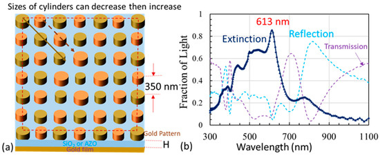
Figure 1.
(a) Schematic of a 6 ΛS × 6 ΛS unit cell of graded photonic super-crystal (GPSC) with gold cylinders. (b) Simulated reflection, transmission and extinction for Au GPSC on a glass slide.
3. Multiple-Band Absorption in Au/SiO2/Au Patterned with GPSC
Figure 1b shows the simulated reflection (R) and transmission (T) from Au GPSC on dielectric SiO2 (without the Au film). The extinction (E) is obtained by E = 1-T-R. The transmission spectrum shows a low transmission window between 400 and 600 nm. There is a low reflection window between 400 and 720 nm in the reflection in Figure 1b. The calculated extinction shows a sharp peak at 613 nm and a broad band centered around 557 nm, similar to the plasmonic features observed in gold nanorods [45]. There are weak peaks around 391, 440 and 775 nm. In GPSC, the cylinders on the edge of the unit super-cell have almost same sizes, and the percentage of these cylinders over the total number of cylinders is high. The size of cylinders becomes smaller or bigger near the center, and these cylinders have a low percentage over the total number of cylinders. The bigger the size of the cylinders, the larger the plasmonic resonance wavelength following Equation (2) [6,45]:
where D is the diameter of cylinders, neff is the effective index for the SPP, k is an integer number and θ is the phase shift due to the SPP mode reflection. The diameter of cylinders on the edge is approximately 90 nm [42], corresponding to a localized surface plasmonic resonance wavelength of 558 nm [3] and coupled surface plasmonic resonance wavelength of around 583 nm assuming a reflection phase θ = 0.29 and k = 1 in Equation (2) [6]. The plasmonic resonance wavelength can reach 793 nm for the large cylinder with a diameter of 158 nm. The high extinction between 500 and 640 nm is in agreement with the high percentage of cylinders at the edge over the total.
When the Au film is added below the SiO2 spacer as a metal/insulator/metal structure patterned with GPSC, as shown in Figure 1a, multiple absorption bands appear above 620 nm (as shown in Figure 2a) besides the broadband absorption between 400–600 nm. The absorption peaks are located at 624, 841 and 1464 nm when the thickness of SiO2 is 10 nm. These three peaks increase in wavelength, as indicated by dashed red, blue and purple arrows, as the thickness of the spacer increases from 10 to 15 and 30 nm. These three peaks have wavelengths of (699, 904, 1625 nm) and (819, 988, 1776 nm) for a space thickness of 15 and 30 nm, respectively. These three peaks can be assigned as gap SPP following Equation (3), which is similar to Equation (2) [6,45,46]:
where P is the propagation length along the [n, m] direction, and neff-Au-Spacer is the effective index for the SPP at the interface of the gold film and SiO2. The effective refractive index neff-Au-Spacer can be obtained from Equation (4) [46]:
where and are the permittivity of gold and SiO2, respectively. In the direction of [n, m] = [1, 0] and using k = 1 and the reflection phase θ = 0.29, the gap SPP wavelength is calculated to be 650 nm using Equations (3) and (4). The gap SPP wavelength is calculated to be 858 and 1653 nm in the direction of [n, m] = [1, 1] for the propagation distance of and , respectively. The calculated SPP wavelengths are (650, 858 and 1653 nm) when compared with the simulated SPP wavelengths of (624, 841 and 1464 nm) for a spacer thickness of 10 nm in Au/SiO2/Au patterned with GPSC. When the thickness is increased, these three peaks are red-shifted. It should be mentioned that the effective index for gap plasmon depends on the MIM spacer thickness in metamaterial MIM structures [47,48,49].
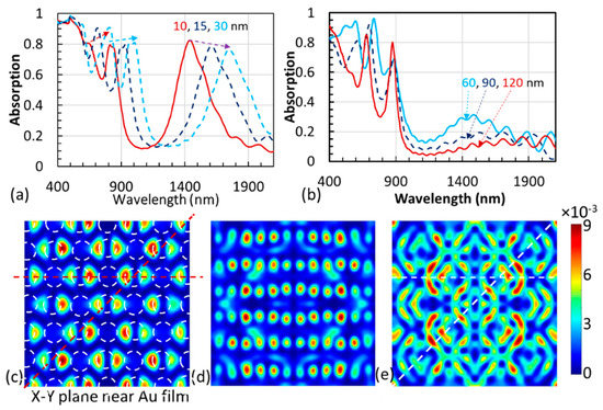
Figure 2.
(a) Multiple-band absorption due to gap SPP in Au/SiO2/Au patterned with GPSC when the SiO2 thickness is 10 (solid red line), 15 (dashed dark-blue line) and 30 nm (dashed light-blue line). (b) Absorption in Au/SiO2/Au patterned with GPSC when the SiO2 thickness is 60 (solid light-blue line), 90 (dashed dark-blue line) and 120 nm (solid red line). E-field intensity in the X-Y plane inside the spacer (c) near the Au film, (d) in the middle of the spacer, and (e) inside the spacer near Au GPSC, in a stack of Au-GPSC/20-nm-SiO2/Au film. These E-field intensities are excited by a Gaussian source with a central wavelength of 1400 nm.
When the thickness of the spacer SiO2 reaches 60 nm, the peak around 1450 nm becomes very weak, as shown in Figure 2b. When further increasing the thickness to 90 and 120 nm, the peak completely disappears due to the weak confinement of a gap SPP with a large gap and a long propagation length [45]. The gap SPPs do still exist but are not efficiently coupled to the resonator.
Figure 2c shows the E-field intensity in the X-Y plane inside the spacer near the Au film in a stack of Au-GPSC/20-nm-SiO2/Au film. The dashed white circles indicate the lattice location for Au GPSC. The dashed red lines indicate the horizontal and [1, 1] directions. Within 20 nm from the Au GPSC, the E-field intensity has a pattern with a symmetry similar to the GPSC lattice. The E-field oscillates near locations underneath golden cylinders (one set of lattices in Figure 1a), in the x-direction following the x-polarization of light. Figure 2d shows the E-field intensity in the X-Y plane in the middle of the spacer. Gap SPP modes are clearly observed. The E-field intensity in the X-Y plane inside the spacer near Au GPSC is shown in Figure 2e. Both oscillations in the horizontal and [1, 1] directions in the E-field intensity are presented with an eye-guidance from the dashed white lines. Due to two sets of lattices in GPSC, it is reasonable to have an E-field coupling along the [1, 1] direction with the same set of motifs in the lattice when compared with the diffraction orders of (1, 1), (1, −1), (−1, −1) and (−1, −1) observed in the diffraction pattern from Al GPSC [42]. Due to the fact that there is SPP coupling near Au GPSC in Figure 2e while the coupling in the [1, 1] direction in Figure 2c is weak with a distance from Au GPSC, the gap SPP coupling with resonators at a long propagation distance in the [1, 1] direction will become weak when the thickness of the spacer is increased. This is why the absorption peak around 1600 nm disappears in Figure 2a,b when the spacer thickness is increased to be larger than 60 nm.
4. Broadband Absorption in Au/Absorbing-Spacer/Au Patterned with GPSC
In order to achieve a broad absorption in near-infrared, we replace SiO2 with a weakly absorbing material that has a complex refractive index n + ik with k << n. The dielectric function of the material can be obtained by the Drude−Lorentz oscillator model in Equation (5):
where the background permittivity , the plasma frequency , the carrier relaxation rate and , representing the strength of the Lorentz oscillator with a center frequency and relaxation . These permittivity parameters are adopted from the spectra ellipsometry on AZO with different Al-doping [50]. AZO or ITO is popular as an electrically tunable and transparent conducting material for tunable MIM devices [51]. Figure 3 shows the calculated real (n) and imaginary (k) parts of the refractive index in the wavelength range between 500 and 4500 nm. k << n, as shown in the figure. The imaginary part k increases from zero at a low wavelength to 0.002 at 1260 nm, to 0.005 at 1698 nm, to 0.01 at 2120 nm, and then to 0.02 at 2630 nm. Correspondingly, the real part n decreases from 1.82 to 1.78, 1.74, 1.69 and then to 1.61. We also plot n and k in Figure 3 for a carrier relaxation rate 0.14 eV and 0.28 eV while the other parameters are same. The carrier relaxation rate in the Drude model in Equation (5) is related to the optical loss. When increases, k increases in Figure 3.
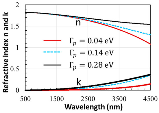
Figure 3.
The real (n) and imaginary (k) parts of the refractive index for a wavelength range between 500 and 4500 nm for carrier relaxation rates of 0.04, 0.14 and 0.28 eV in Equation (5).
Figure 4a shows the absorption for a spacer thickness of 80, 120 and 350 nm in a stack of Au-GPSC/weakly-absorbing-spacer/Au-film. For thicknesses of 80 and 120 nm, broadband absorption appears around 1400–2300 nm, where peaks are disappearing in Figure 2b. Considering the refractive index and Fabry–Pérot (F-P) effect, the optical path length of 120 nm × 1.5 (1.5 is the refractive index) in Figure 2b corresponds to the optical path length of 100 nm × 1.8 in Figure 4a. The difference in absorption in near-infrared between the two figures can be due to the weakly absorbing spacer used in Figure 4a.
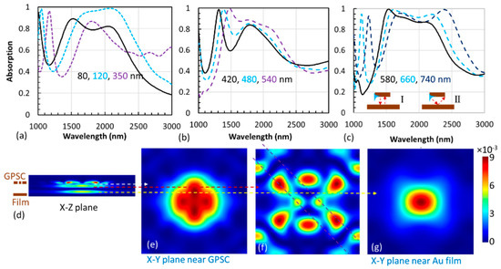
Figure 4.
Simulated absorption in a stack of Au-GPSC/weakly-absorbing-spacer/Au-film with a spacer thickness of (a) (80, 120, 350 nm), (b) (420, 480, 540 nm) and (c) (580, 660, 740 nm). (d) E-field intensity in a cross section in the X-Z plane for a space thickness of 350 nm. (e–g) E-field intensity in a cross section in the X-Y plane through z-locations indicated by dashed white, red and yellow arrows, respectively. These E-field intensities are excited by a Gaussian source with a central wavelength of 1900 nm.
The F-P resonance in Figure 4 can form inside the spacer between Au-GPSC and the Au film through a possible F-P cavity length (FPCL), as shown in Equations (6)–(8) [52,53,54]:
where T is the thickness of the spacer, D is the diameter of the cylinder in GPSC and is the lattice period in the [n, m] direction. Equation (6) is for the F-P resonance diffracted by the GPSC grating from different directions, while Equations (7) and (8) are for F-P between Au-cylinders and Au-film, as shown by the inserts in Figure 4c for type II and type I, respectively. The formation of the F-P resonance meets the following condition in Equation (9) [53,55]:
where φtop and φbottom are the additional phase shifts at the top and bottom surfaces, respectively, due to the reflection and penetration depth. With a penetration depth of 26 nm around 1900 nm in Au, φ = 0.06. We use φtop + φbottom = 0.29 + 0.06 for the path in Equations (6) and (7) and φtop + φbottom = 0.06 + 0.06 for the path in Equation (8). Using these additional phase shifts, the calculated wavelength for the absorption peak is close to the simulated one.
Based on Equations (6)–(9), SPP and F-P coupling in the [1, 1] direction gives an absorption centered around 1962 nm for a spacer thickness of 120 nm, in agreement with the simulated broadband absorption wavelength between 1600 and 2200 nm and the central wavelength of 1975 nm indicated by the dashed green square in Figure 5. For a thickness of 420 nm in Figure 4b, the absorption is calculated to be 1780 nm using Equation (8). The absorption is around 2200 and 2050 nm for a spacer thickness of 580 nm in Figure 4c using Equations (7) and (8), respectively.
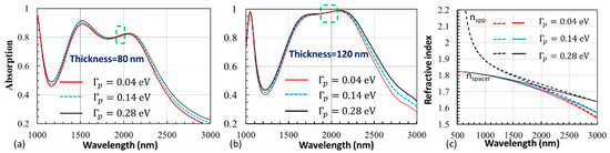
Figure 5.
Simulated absorption in a stack of Au-GPSC/weakly-absorbing-spacer/Au-film with a spacer thickness of (a) 80 nm and (b) 120 nm for carrier relaxation rates of 0.04, 0.14 and 0.28 eV in Equation (5) for an AZO spacer. (c) Dispersion of the refractive index nspp and nAZO with carrier relaxation rates of 0.04, 0.14 and 0.28 eV in Equation (5) for an AZO spacer.
Figure 4d shows the E-field intensity in a cross section in the X-Z plane for a space thickness of 350 nm in a stack of Au-GPSC/weakly-absorbing-spacer/Au-film. The E-field intensity is high near the center of the unit super-cell of GPSC, and F-P resonance appears between Au-GPSC and Au-film. Figure 4e shows the E-field intensity in a cross section in the X-Y plane through z-locations indicated by the dashed white arrow (just below Au-GPSC). A square pattern appears following the GPSC symmetry. In the middle of the spacer, the E-field intensity shows oscillations along the [1, 1] direction, as indicated by dashed purple lines. The light is reflected by the Au film at the center of the unit super-cell, as shown in Figure 4g. Thus, the coupling of SPP and F-P resonance leads to a broadband absorption in near-infrared in the stack of Au-GPSC/weakly-absorbing-spacer/Au-film. For thin device applications, a space thickness of 120 nm, as shown in Figure 4a, can have a broadband absorption in near-infrared.
5. Discussion
Although super-lattice, complex motifs or multiple resonators have been placed in a unit cell of MIM structures by other research groups [25,26,27,28,29,30,31], the broad absorption around 1400–2100 nm has not been reported. We believe that the coupling of SPP with GPSC resonators in [±1, ±1] directions plays a key role in the appearance of the broad absorption band around 1400–2100 nm in our GPSC-based MIM, as evidenced by the E-field intensity here and the reported laser diffraction in [±1, ±1] from the GPSC pattern [42]. Due to the dual lattice feature (as indicated by arrows in Figure 1a for GPSC) the SPP is forced to propagate and resonate in the [1, 1] direction. Due to different diameters for cylinders in GPSC, the SPP has a broadband resonance.
We believe that the material dispersion also plays a role in the coupling of SPP with F-P resonance in the spacer. Adopting the permittivity in Equation (5) and in Figure 3 for AZO, we simulate the absorption of Au-GPSC/weakly-absorbing-spacer/Au-film for carrier relaxation rates of 0.04 (red line), 0.14 (blue dash) and 0.28 eV (black line), as shown in Figure 5a,b for a spacer thickness of 80 nm and 120 nm, respectively. As expected, the absorption increases with an increasing k (increasing Γp) in both Figure 5a,b. However, the absorption is almost the same between the wavelengths of 1916 and 2014 nm in Figure 5a and between 1860 and 2090 nm in Figure 5b, as indicated by the dashed green rectangle and square in the figure, respectively. These dashed green rectangle and square are centered at 1965 and 1975 nm, respectively. This indicates that the SPP wavelength is around 1970 nm and that it is mainly related to the Au permittivity and GPSC structure. The broadband coupling between SPP and F-P resonance can be understood from the dispersion of nspp and nspacer, as shown in Figure 5c. These nspp and nspacer values are very close and change with the wavelength, having almost the same slope between 1700 and 2200 nm.
6. Conclusions
In summary, we have observed multiband absorption in a stack of Au-GPSC/SiO2/Au-film. The absorption band near 1500 nm is assigned to the gap SPP in the [1, 1] direction. This feature appears in the stack that is patterned in GPSC due to its dual-lattice structure and the coupling of SPP along one set of the lattice in the [1, 1] direction. Broadband absorption has been observed in a stack of Au-GPSC/weakly-absorbing-spacer/Au-film due to SPP and F-P resonance in the [1, 1] direction. The E-field intensity has been simulated for both stacks, for which SPP and F-P resonance have been confirmed. The E-field intensity has also confirmed the formation of gap SPP near 1500 nm when the spacer thickness was below 30 nm.
Author Contributions
Y.L., J.C. and H.Z. conceived the concepts; Y.L., S.K. and S.H. designed simulations; S.K., S.H. and K.A. performed the simulations; Y.L., S.K. and S.H. analyzed the data and wrote the paper. All authors have read and agreed to the published version of the manuscript.
Funding
This work is supported by research grants from the U.S. National Science Foundation under Grant Nos. CMMI-1661842 and 1661749.
Data Availability Statement
Data will be available upon request.
Acknowledgments
We thank Noah Hurley for improving the English in the manuscript.
Conflicts of Interest
The authors declare no conflict of interest. The funders had no role in the design of the study; in the collection, analyses, or interpretation of data; in the writing of the manuscript, or in the decision to publish the results.
References
- Zhao, J.; Wang, Y.; Zhu, Y.; Zhang, W.; Yu, Y. Lithography-free flexible perfect broadband absorber in visible light based on an all-dielectric multilayer structure. Opt. Lett. 2020, 45, 5464–5467. [Google Scholar] [CrossRef]
- Anker, J.N.; Hall, W.P.; Lyandres, O.; Shah, N.C.; Zhao, J.; Van Duyne, R.P. Biosensing with plasmonic nanosensors. Nat. Mater. 2008, 7, 442–453. [Google Scholar] [CrossRef]
- Cao, J.; Sun, T.; Grattan, K.T.V. Gold nanorod-based localized surface plasmon resonance biosensors: A review. Sens. Actuators B Chem. 2014, 95, 332–351. [Google Scholar] [CrossRef]
- Chong, Y.D.; Cao, L.; Ge, H.; Stone, A.D. Coherent perfect absorbers: Time-reversed lasers. Phys. Rev. Lett. 2010, 105, 053901. [Google Scholar] [CrossRef] [PubMed]
- Fang, Z.; Zhen, Y.R.; Fan, L.; Zhu, X.; Nordlander, P. Tunable wide-angle plasmonic perfect absorber at visible frequencies. Phys. Rev. B 2012, 85, 245401. [Google Scholar] [CrossRef]
- Nielsen, M.G.; Pors, A.; Albrektsen, O.; Bozhevolnyi, S.I. Efficient absorption of visible radiation by gap plasmon resonators. Opt. Express 2012, 20, 13311–13319. [Google Scholar] [CrossRef] [PubMed]
- Luk, T.S.; Fofang, N.T.; Cruz-Campa, J.L.; Frank, I.; Campione, S. Surface Plasmon polariton enhanced ultrathin nano-structured CdTe solar cell. Opt. Express 2014, 22, A1372–A1379. [Google Scholar] [CrossRef] [PubMed]
- Chen, H. Interference theory of metamaterial perfect absorbers. Opt. Express 2012, 20, 7165–7172. [Google Scholar] [CrossRef]
- Aydin, K.; Ferry, E.V.; Briggs, M.R.; Atwater, H.A. Broadband polarization-independent resonant light absorption using ultrathin plasmonic super absorbers. Nat. Commun. 2011, 2, 517. [Google Scholar] [CrossRef]
- Sun, T.; Guo, C.F.; Cao, E.M.; Akinoglu, Y.; Wang, M.; Giersig, Z.R.; Kempa, K. A broadband solar absorber with 12 nm thick ultrathin a-Si layer by using random metallic nanomeshes. Appl. Phys. Lett. 2014, 104, 251119. [Google Scholar] [CrossRef]
- Sturmberg, B.C.P.; Chong, T.K.; Choi, D.Y.; White, T.P.; Botten, L.C.; Dossou, K.B.; Poulton, C.G.; Catchpole, K.R.; McPhedran, R.C.; de Sterke, C.M. Total absorption of visible light in ultrathin weakly absorbing semiconductor gratings. Optica 2016, 3, 556–562. [Google Scholar] [CrossRef]
- Ghobadi, A.; Hajian, H.; Rashed, A.R.; Butun, B.; Ozbay, E. Tuning the metal filling fraction in metal-insulator-metal ultra-broadband perfect absorbers to maximize the absorption bandwidth. Photon. Res. 2018, 6, 168–176. [Google Scholar] [CrossRef]
- Kats, M.A.; Blanchard, R.; Genevet, P.; Capasso, F. Nanometer optical coatings based on strong interference effects in highly absorbing media. Nat. Mater. 2013, 12, 20–24. [Google Scholar] [CrossRef]
- Kats, M.A.; Byrnes, S.J.; Blanchard, R.; Kolle, M.; Genevet, P.; Aizenberg, J.; Capasso, F. Enhancement of absorption and color contrast in ultra-thin highly absorbing optical coatings. Appl. Phys. Lett. 2013, 103, 101104. [Google Scholar] [CrossRef]
- Yongbing, L.; Runmei, S.; Qiwen, W.; Liang, S.; Bowen, L.; Wenhao, Z. Deducing critical coupling condition to achieve perfect absorption for thin-film absorbers and identifying key characteristics of absorbing materials needed for perfect Absorption. Appl. Phys. Lett. 2014, 104, 091109. [Google Scholar]
- Ding, B.; Qiu, M.; Blaikie, R.J. Manipulating light absorption in dye-doped dielectric films on reflecting surfaces. Opt. Express 2014, 22, 25965–25975. [Google Scholar] [CrossRef] [PubMed]
- Song, H.; Guo, L.; Liu, Z.; Liu, K.; Zeng, D.J.; Zhang, N.; Hu, H.; Jiang, S.; Gan, Q. Nanocavity enhancement for ultra-thin film optical absorber. Adv. Mater. 2014, 26, 2737–2743. [Google Scholar] [CrossRef] [PubMed]
- Li, Z.; Butun, S.; Aydin, K. Large-area lithography-free super absorbers and color filters at visible frequencies using ultrathin metallic films. ACS Photonics 2015, 2, 183–188. [Google Scholar] [CrossRef]
- Li, Z.; Palacios, E.; Butun, S.; Kocer, H.; Aydin, K. Omnidirectional broadband light absorption using large- area ultrathin lossy metallic film coatings. Sci. Rep. 2015, 5, 15137. [Google Scholar] [CrossRef]
- Lee, K.T.; Seo, S.; Lee, J.Y.; Guo, L.J. Strong resonance effect in a lossy medium-based optical cavity for angle robust spectrum filters. Adv. Mater. 2014, 26, 6324–6328. [Google Scholar] [CrossRef]
- Streyer, W.; Law, S.; Rooney, G.; Jacobs, T.; Wasserman, D. Strong absorption and selective emission from engineered metals with dielectric coatings. Opt. Express 2013, 21, 9113–9122. [Google Scholar] [CrossRef] [PubMed]
- Lee, K.T.; Ji, C.; Guo, L.J. Wide-angle, polarization-independent ultrathin broadband visible absorbers. Appl. Phys. Lett. 2016, 108, 031107. [Google Scholar] [CrossRef]
- Kocer, H.; Butun, S.; Li, Z.; Aydin, K. Reduced near-infrared absorption using ultra-thin lossy metals in Fabry-Perot cavities. Sci. Rep. 2015, 5, 8157. [Google Scholar] [CrossRef] [PubMed]
- Mirshafieyan, S.S.; Luk, T.S.; Guo, J. Zeroth order Fabry-Perot resonance enabled ultra-thin perfect light absorber using percolation aluminum and silicon nanofilms. Opt. Mater. Express 2016, 6, 1032–1042. [Google Scholar] [CrossRef]
- Zhang, B.; Hendrickson, J.; Guo, J. Multispectral near perfect metamaterial absorbers using spatially multiplexed plasmon resonance metal square structures. J. Opt. Soc. Am. B 2013, 30, 656–662. [Google Scholar] [CrossRef]
- Hendrickson, J.; Guo, J.B.; Zhang, W.B.; Soref, R. Wideband perfect light absorber at midwave infrared using multiplexed metal structures. Opt. Lett. 2012, 37, 371–373. [Google Scholar] [CrossRef] [PubMed]
- Song, Y.; Wang, C.; Lou, Y.; Cao, B.; Li, X. Near-perfect absorber with ultrawide bandwidth in infrared region using a periodically chirped structure. Opt. Commun. 2013, 305, 212. [Google Scholar] [CrossRef]
- Palanchoke, U.; Boutami, S.; Pocas, S.; Rochat, N.; Goudon, V.; Rabaud, W. Influence of dimensional variation of metal-insulator-metal stack in spectral response. Opt. Mater. Express 2018, 8, 2494–2509. [Google Scholar] [CrossRef]
- Nagarajan, A.; Vivek, K.; Shah, M.; Achanta, V.G.; Gerini, G. A Broadband Plasmonic Metasurface Superabsorber at Optical Frequencies: Analytical Design Framework and Demonstration. Adv. Opt. Mater. 2018, 6, 1800253. [Google Scholar] [CrossRef]
- Azad, A.K.; Kort-Kamp, W.J.M.; Sykora, M.; Weisse-Bernstein, N.R.; Luk, T.S.; Taylor, A.J.; Dalvit, D.A.R.; Chen, H. Metasurface Broadband Solar Absorber. Sci. Rep. 2016, 6, 20347. [Google Scholar] [CrossRef]
- Pors, A.; Albrektsen, O.; Radko, I.R.; Bozhevolnyi, S.I. Gap plasmon-based metasurfaces for total control of reflected light. Sci. Rep. 2013, 3, 2155. [Google Scholar] [CrossRef]
- Lowell, D.; Lutkenhaus, J.; George, D.; Philipose, U.; Chen, B.; Lin, Y. Simultaneous direct holographic fabrication of photonic cavity and graded photonic lattice with dual periodicity, dual basis, and dual symmetry. Opt. Express 2017, 25, 14444–14452. [Google Scholar] [CrossRef]
- Lowell, D.; Hassan, S.; Adewole, M.; Philipose, U.; Chen, B.; Lin, Y. Holographic fabrication of graded photonic super-crystals using an integrated spatial light modulator and reflective optical element laser projection system. Appl. Opt. 2017, 56, 9888. [Google Scholar] [CrossRef]
- Lowell, D.; Hassan, S.; Sale, O.; Adewole, M.; Hurley, N.; Philipose, U.; Chen, B.; Lin, Y. Holographic fabrication of graded photonic super-quasi-crystal with multiple level gradients. Appl. Opt. 2018, 57, 6598. [Google Scholar] [CrossRef]
- Hassan, S.; Sale, O.; Lowell, D.; Hurley, N.; Lin, Y. Holographic fabrication and optical property of graded photonic super-crystals with a rectangular unit super-cell. Photonics 2018, 5, 34. [Google Scholar] [CrossRef]
- Sale, O.; Hassan, S.; Hurley, N.; Alnasser, K.; Philipose, U.; Zhang, H.; Lin, Y. Holographic fabrication of octagon graded photonic super-crystal and potential applications in topological photonics. Front. Optoelectron. 2020, 13, 12–17. [Google Scholar] [CrossRef]
- Hassan, S.; Lowell, D.; Lin, Y. High light extraction efficiency into glass substrate in organic light-emitting diodes by patterning the cathode in graded superlattice with dual periodicity and dual basis. J. Appl. Phys. 2017, 121, 233104. [Google Scholar] [CrossRef]
- Hassan, S.; Alnasser, K.; Lowell, D.; Lin, Y. Effects of Photonic Band Structure and Unit Super-Cell Size in Graded Photonic Super-Crystal on Broadband Light Absorption in Silicon. Photonics 2019, 6, 50. [Google Scholar] [CrossRef]
- Hassan, S.; Sale, O.; Alnasser, K.; Hurley, N.; Zhang, H.; Philipose, U.; Lin, Y. Broadband light-matter interaction due to resonance cavities in graded photonic super-crystals. OSA Contin. 2019, 2, 3272–3280. [Google Scholar] [CrossRef]
- Hassan, S.; Lowell, D.; Adewole, M.; George, D.; Zhang, H.; Lin, Y. Extraordinary light trapping enhancement in silicon solar cell patterned with graded photonic super-crystal. Photonics 2017, 4, 50. [Google Scholar] [CrossRef]
- Alnasser, K.; Hassan, S.; Kamau, S.; Zhang, H.; Lin, Y. Enhanced light extraction from organic light emitting diodes by reducing plasmonic loss through graded photonic super-crystals. J. Opt. Soc. Am. B 2020, 37, 1283. [Google Scholar] [CrossRef]
- Hassan, S.; Jiang, Y.; Alnasser, K.; Hurley, N.; Zhang, H.; Philipose, U.; Lin, Y. Generation of over 1000 Diffraction Spots from 2D Graded Photonic Super-Crystals. Photonics 2020, 7, 27. [Google Scholar] [CrossRef]
- Rakic, A.; Djurisic, A.; Elazar, J.; Majewski, M. Optical properties of metallic films for vertical-cavity optoelectronic devices. Appl. Opt. 1998, 37, 5271. [Google Scholar] [CrossRef] [PubMed]
- Oskooi, F.; Roundy, D.; Ibanescu, M.; Bermel, P.; Joannopoulos, J.D.; Johnson, S.G. MEEP: A flexible free-software package for electromagnetic simulations by the FDTD method. Comput. Phys. Commun. 2010, 181, 687. [Google Scholar] [CrossRef]
- Pors, A.; Bozhevolnyi, S.I. Plasmonic metasurfaces for efficient phase control in reflection. Opt. Express 2013, 21, 27438–27451. [Google Scholar] [CrossRef] [PubMed]
- Maradudin, A.A.; Sambles, J.R.; Barnes, W.L. Handbook of Surface Science Volume 4: Modern Plamnonics; Elsevier: Oxford, UK, 2014. [Google Scholar]
- Koechlin, C.; Bouchon, P.; Pardo, F.; Pelouard, J.-L.; Haïdar, R. Analytical description of subwavelength plasmonic MIM resonators and of their combination. Opt. Express 2013, 21, 7025–7032. [Google Scholar] [CrossRef]
- Toudert, J.; Serna, R.; Pardo, M.G.; Ramos, N.; Peláez, R.J.; Maté, B. Mid-to-far infrared tunable perfect absorption by a sub-λ/100 nanofilm in a fractal phasor resonant cavity. Opt. Express 2018, 26, 34043–34059. [Google Scholar] [CrossRef] [PubMed]
- Yu, P.; Besteiro, L.V.; Huang, Y.; Wu, J.; Fu, L.; Tan, H.H.; Jagadish, C.; Wiederrecht, G.P.; Govorov, A.O.; Wang, Z. Broadband metamaterial absorbers. Adv. Opt. Mater. 2019, 7, 1800995. [Google Scholar] [CrossRef]
- George, D.; Li, L.; Jiang, Y.; Lowell, D.; Mao, M.; Hassan, S.; Ding, J.; Cui, J.; Zhang, H.; Philipose, U.; et al. Localized Surface Plasmon Polariton Resonance in Holographically Structured Al-doped ZnO. J. Appl. Phys. 2016, 120, 043109. [Google Scholar] [CrossRef]
- Park, J.J.; Kang, X.; Liu, M.L. Brongersma. Electrically tunable Epsilon-NearZero (ENZ) metafilm absorbers. Sci. Rep. 2015, 5, 15754. [Google Scholar] [CrossRef] [PubMed]
- Evans, R.N.; Calhoun, S.R.; Brescia, J.R.; Cleary, J.W.; Smith, E.M.; Peale, R.E. Far-infrared bands in plasmonic metal-insulator-metal absorbers optimized for long-wave infrared. MRS Adv. 2019, 4, 667–674. [Google Scholar] [CrossRef]
- George, D.; Adewole, M.; Hassan, S.; Lowell, D.; Cui, J.; Zhang, H.; Philipose, U.; Lin, Y. Coupling of Surface Plasmon Polariton in Al-Doped ZnO with Fabry-Pérot Resonance for Total Light Absorption. Photonics 2017, 4, 35. [Google Scholar] [CrossRef]
- Nath, J.; Modak, S.; Rezadad, I.; Panjwani, D.; Rezaie, F.; Cleary, J.W.; Peale, R.E. Far-infrared absorber based on standing-wave resonances in metal-dielectric-metal cavity. Opt. Express 2015, 23, 20366–20380. [Google Scholar] [CrossRef]
- Cui, Y.; He, Y.; Jin, Y.; Ding, F.; Yang, L.; Ye, Y.; Zhong, S.; Lin, Y.; He, S. Plasmonic and Metamaterial Structures as Electromagnetic Absorbers. Laser Photonics Rev. 2014, 8, 495–520. [Google Scholar] [CrossRef]
Publisher’s Note: MDPI stays neutral with regard to jurisdictional claims in published maps and institutional affiliations. |
© 2021 by the authors. Licensee MDPI, Basel, Switzerland. This article is an open access article distributed under the terms and conditions of the Creative Commons Attribution (CC BY) license (https://creativecommons.org/licenses/by/4.0/).