Review

Silicon-Based Optoelectronics Enhanced by Hybrid Plasmon Polaritons: Bridging Dielectric Photonics and Nanoplasmonics

1
State Key Laboratory of Advanced Optical Communication Systems and Networks, Department of Electronics, School of Electronics Engineering and Computer Science, Peking University, Beijing 100871, China
2
Shenzhen Research Institute, Peking University, Shenzhen 518057, China
3
Nano-Optoelectronics Frontier Center of Ministry of Education, Peking University, Beijing 100871, China
4
Shanghai Institute of Optics and Fine Mechanics, Chinese Academy of Sciences, Shanghai 201800, China
*
Author to whom correspondence should be addressed.
Photonics 2021, 8(11), 482; https://doi.org/10.3390/photonics8110482
Submission received: 8 September 2021 / Revised: 13 October 2021 / Accepted: 13 October 2021 / Published: 28 October 2021

Abstract

:
Silicon-based optoelectronics large-scale integrated circuits have been of interest to the world in recent decades due to the need for higher complexity, larger link capacity, and lower cost. Surface plasmons are electromagnetic waves that propagate along the interface between a conductor and a dielectric, which can be confined several orders smaller than the wavelength in a vacuum and offers the potential for minimizing photonic circuits to the nanoscale. However, plasmonic waveguides are usually accompanied by substantial propagation loss because metals always exhibit significant resistive heating losses when interacting with light. Therefore, it is better to couple silicon-based optoelectronics and plasmonics and bridge the gap between micro-photonics and nanodevices, especially some nano-electronic devices. In this review, we discuss methods to enhance silicon-based optoelectronics by hybrid plasmon polaritons and summarize some recently reported designs. It is believed that by utilizing the strong light confinement of plasmonics, we can overcome the conventional diffraction limit of light and further improve the integration of optoelectronic circuits.

1. Introduction

1.1. Silicon-Based Optoelectronics
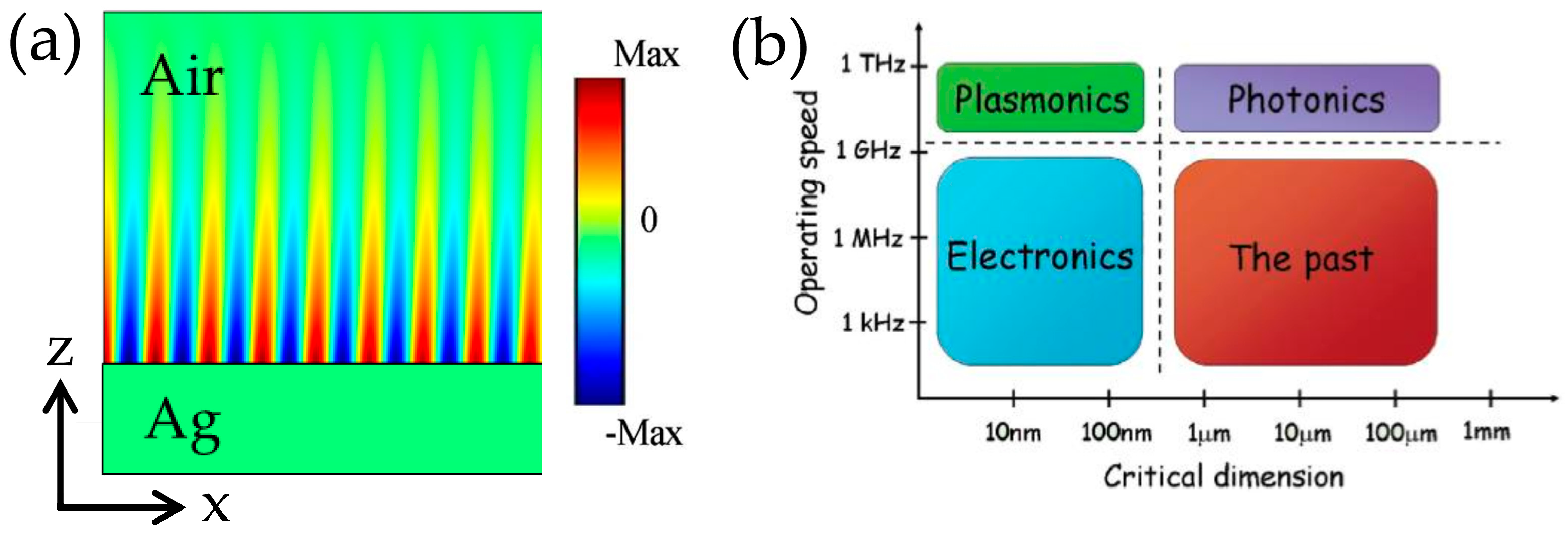
The development of optoelectronic devices has affected many aspects of society, from simple household appliances and multimedia systems to communications, computers, and medical equipment. The main characteristics of the next-generation optical communication system will be intelligence, integration, low cost, and high reliability. At the same time, with the rapid development of high-performance computers, the central processing unit (CPU) speed will be faster, and the memory storage space will be larger. Therefore, high-density data communication in the computer system has become the main bottleneck restricting its development. Currently, optical interconnection is recognized as an important development direction for realizing high-speed communication between computers and even chips. Due to the above-mentioned requirements for the development of optical communications and computers, people have a keen interest in the development of micro-nano-sized devices that can provide more functions and better performance.
However, the materials used in optoelectronic devices are diverse, such as III–V group compounds (InP, GaAs) and group IV materials (Si, Ge). The fabrication processes of various material platforms are different from each other. Therefore, it is hard to integrate them together. Fortunately, the price of silicon materials is very low, and silicon-based micro-nano processing technology developed by the integrated circuit industry is very mature. This gives people hope to make silicon-based micro-nano photonic devices. Then, silicon photonic devices and logic circuits can be integrated on the same chip. In this way, the high-density data communication capability of the computer system can be greatly improved, while the size, power consumption, and cost of the system will be significantly reduced.
Silicon-based optoelectronics is a chip-size solution based on the interaction between photons and electrons, developed on the traditional microelectronics platform. Since Richard A. Soref’s early work about the electro-optic effect of silicon in 1985, silicon-based optoelectronics have been on a rapid development track. Many breakthroughs have been made on the fundamental components of the silicon-based optoelectronics platform, such as on-chip light sources [1], modulators [2,3], multiplexing technologies [4,5], light coupling [6,7], polarization handling [8], and light detection [9,10]. Several important works of silicon-based optoelectronics in the past few decades are shown in Figure 1.
In 2004, Yurii et al. designed and fabricated low loss CMOS-compatible silicon strip waveguides [13], which are most commonly used for light guiding. In 2006, 2007, and 2009, on-chip lasers [14], optical modulators [17], and photon detectors [18] for silicon-based optoelectronics were reported by Intel. These basic devices are indispensable for researches on modules. After 2010, some research institutions (Intel, IBM, etc.) [12,15,16,19] manufactured high-speed and broadband optical transceivers, which are greatly demanded in date center short-reach interconnection nowadays [20]. According to the ‘More than Moore’ roadmap [21], integrating processing units and optical transceivers on a monolithic chip is the future trend after Moore’s Law. In 2015, a single-chip microprocessor communicating directly using light was reported [11], which realized CMOS-compatible chip-scale electronic–photonic systems for the first time.

1.2. Plasmonics

Plasmonics has become a promising technology that can overcome the diffraction limits of dielectric photonics [22,23,24,25,26,27]. Propagating along the interface between a conductor and a dielectric material, surface plasmons are mixing of photons and plasmons (in the conductor) [28,29]. The term ‘surface plasmons’ (SPs) was first used by Ritchie in 1957 when he extended the work of Pines and Bohm [30]. Since then, surface plasmons have gone by several names in the literature. The term ‘surface plasmon polaritons’ (SPPs) is also frequently used in many areas. The word ‘polaritons’ means the polar excitation in material mixing with the photon, emphasizing that the electromagnetic field is connected to the electronic excitation in the metal.
Figure 2a illustrates the surface plasmons waves propagating along the interface of silver and air. The electromagnetic field is localized on the surface of silver, and the free electrons in the silver oscillate in resonance with the optical field in the air. These optical waves are trapped on the surface and help us to channel and manipulate on a subwavelength scale. It could lead to photonic circuits with footprints much smaller than those traditional dielectric ones. The relationship of semiconductor electronics, dielectric photonics, and plasmonics is illustrated in Figure 2b, in which the dashed lines indicate the limitations of these technologies. Semiconductor electronics are limited by interconnect delay time and heat generation issues with an operating speed of about 10 GHz. The diffraction limit prohibits dielectric photonics from achieving critical dimensions comparable with microelectronics. Plasmonics can be guided beyond the diffraction limit and serve as a bridge between semiconductor nanoelectronics and photonics [31].

1.2.1. Fundamental Principles of Plasmonics

Plasma is hot ionized gas with free charges and is usually named the fourth state of matter. Actually, plasma exists in our daily lives [32,33,34,35] but often needs high temperature and pressure. At room temperature, it is too cold and dense for classical plasma to exist. However, in metal, electrons are delocalized from ions. This means that we can treat metal as a material with plasmons inside. According to the electromagnetic field theory, the relative permittivity of metal can be described approximately by the Drude model [36]:
ε ( ω ) = 1 ω p 2 ω 2 + i γ ω , ω p = N e 2 ε 0 m
where γ is the damping frequency, ω p is the plasma frequency, N is the density of electrons, and m is the mass of electron. The damping frequency is usually about 100 THz. At optical frequency ω γ , the relative permittivity of metal ε ( ω ) can be simplified as:
ε ( ω ) 1 ω p 2 ω 2
For different frequencies ω , the relative permittivity of the metal ε ( ω ) varies, and the metal appears to have different properties (summarized in Table 1).
For surface plasmons γ ω < ω p , the real part of permittivity ε is less than zero, and the imaginary part of permittivity ε is approximately equal to zero. This means the refractive index n of metal is imaginary, and fields decay exponentially in the metal. A variety of theories for surface plasmons have been developed in the literature. Someone might define surface plasmons with quantum mechanics as particles with quantized energy and momentum [37]. However, the classical Maxwell’s equation and electromagnetic model can describe most of the properties of surface plasmons satisfactorily. Though quantum mechanics potentially exist in the background, we can roll it up to the dielectric function in most cases. Practically, it is found that in the surface plasmons system, the bulk dielectric constant can describe the object down to ~10 nm accurately [38]. For most photonic devices on chip, typically, the footprints are much larger. Usually, the classical electromagnetic theory can fully explain the function of the devices, and some numerical calculation methods, such as the finite element method (FEM) and finite difference time domain method (FDTD), are applied to simulate the field profile of surface plasmons.

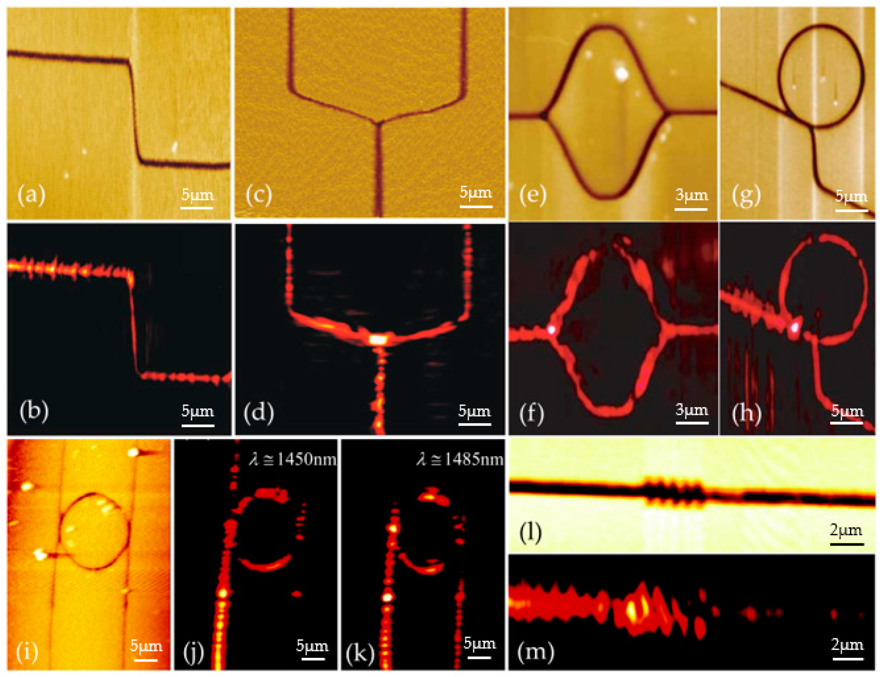
1.2.2. Surface Plasmon Subwavelength Optics

Solving Maxwell’s equations under the boundary conditions, we can derive the dispersion relation of surface plasmons [39]:
k sp = k 0 ε d ε m ( ω ) ε d + ε m ( ω )
where k 0 is the free-space wave vector, ε d is the relative permittivities of dielectric, and ε m is the frequency-dependent permittivity of the metal. According to the boundary conditions [28], if the interface is able to support propagation of surface plasmons, the permittivity of the medium on the different side of the interface necessarily have opposite signs. As shown in Table 1, metals can satisfy this condition because ε m is approximately a negative number for optical frequency. Based on Equation (3), the dispersion curve for surface plasmons mode is depicted in Figure 3. At very low frequency, the dispersion curve tends to the light line in the dielectric. As the frequency increases, the wave vector of surface plasmons approaches infinity. The frequency limit is called the characteristic surface plasmons frequency:
ω sp = ω p 1 + ε d
The high wave vector k sp means that the wavelength of surface plasmons λ sp is smaller than light in the dielectric. This reveals the subwavelength characteristic of surface plasmons, which provides a method to overcoming the Abbe’s diffraction limit [40], and spawns a variety of new technologies to deliver, control, and manipulate electromagnetic radiation on the nanoscale.
The use of surface plasmons has led to the development of abundant nano-optical techniques [41,42], such as surface-enhanced Raman scattering (SERS) [43] for optical sensing of individual molecules [44,45,46], optical nanoscopy, and spectroscopy to achieve super-resolution and unravel the structure–function of materials as tiny as a few nanometers [47,48,49].
In this process, the plasmonic light concentrators that can focus electromagnetic radiation and optical energy to a localized tiny area have attracted the attention of many researchers [50]. Some researchers have reported nanofocusing structures that can squeeze light into a focal spot as small as possible [51]. By using chirped surface gratings [52], plasmonic Fresnel zone plate [53,54], nano-slit arrays [55,56], or other similar periodic optical elements [57,58], the light beam can be concentrated to a little spot in space. These configurations are able to enhance light intensity out-of-plane in free space by tens of thousands of times [41], which shows the superiority of surface plasmons to concentrate light far beyond the diffraction limit. However, in most circumstances, we need to focus light in-plane for practical use [33,59]. One way is to modulate the phase of optical waves and generate a focused spot at some distance. This principle is similar to that used to concentrate light in free space. For example, by arranging holes [60], condensers [61], or slits [62] in curved shapes, the phase fronts of surface plasmon waves will be concaved. As a result, the light is focused in-plane on the metal surface. Another way is to use tapered structures that support surface plasmons. The taper gradually concentrates the field and enhances the intensity of surface plasmons as the light propagates to the apex of the taper. Various types of tapered nanofocusing structures have been reported, such as a conical metal rod with a tiny tip [63,64,65,66], a metal wedge on a dielectric substrate [67,68,69,70], a dielectric wedge on a metal substrate [71,72], etc. Typically, these tapered structures are based on metal–insulator–metal (MIM) or insulator–metal–insulator (IMI) configurations. The MIM structures usually have better optical confinement and a smaller mode area, whereas the IMI structures often have a lower loss and larger propagation length [22,24]. Besides the structures of the taper, the taper angles also influence the physical processes. If the taper angles are sufficiently small, the propagating electromagnetic waves do not ‘feel’ the variation of the taper. Therefore, the reflection and scattering of light are negligible. This is the so-called adiabatic condition [63,73]. Generally speaking, if the variation of the light wavelength is slow enough relative to its wavelength [74,75,76], we can treat the taper as an adiabatic one, by which the energy losses can be significantly reduced during the nanofocusing processes. Some representative functional plasmonic subwavelength waveguide components reported are shown in Figure 4.
Besides the plasmonic light concentrators illustrated above, the plasmonic waveguide components that can find their very practical use in large-scale integrated optical circuits have also generated tremendous interest [80,81,82,83]. Unlike light concentrators, these plasmonic waveguide components support the propagation of electromagnetic waves for a long distance while the light field is bound in a small area. These ultracompact functional plasmonic components utilize channel plasmon polaritons (CPPs), where the electromagnetic waves are confined on the bottom of V-shaped grooves cut into a metal [84,85,86]. At telecom wavelengths, the CPPs can propagate about tens of micrometers while showing relatively strong confinement. Therefore, CPP-based extremely sharp bends and even more sophisticated components (such as waveguide–ring resonator-based add-drop multiplexer and Bragg grating filter shown in Figure 4i,l) have been realized in experiments [77,78,79].

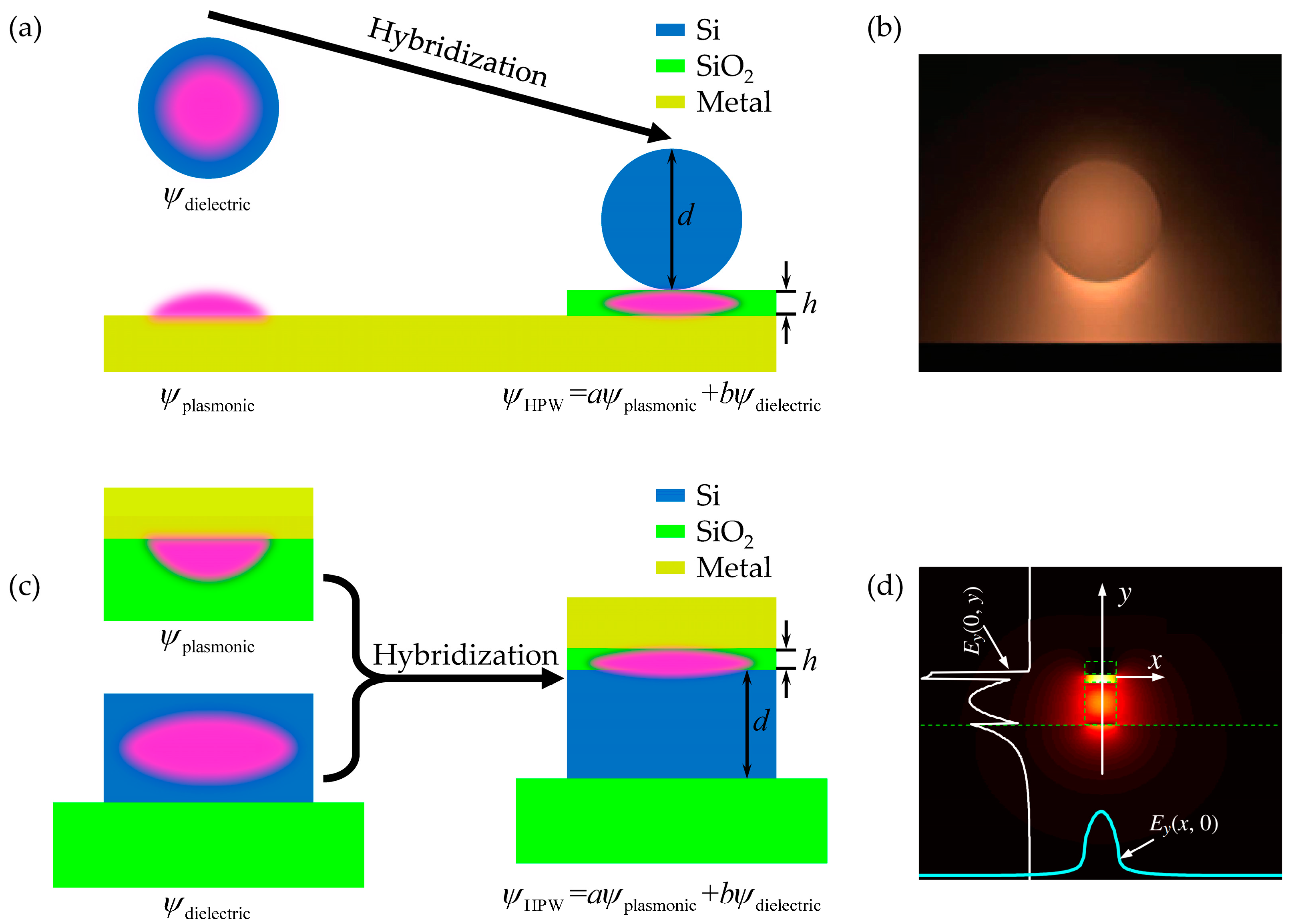
2. Hybrid Plasmon Polaritons (HPPs)

The use of surface plasmons opens up the prospect of extreme light concentration and manipulation. The unprecedented ability of plasmonic devices paves the way for generating [83,87], guiding, modulating [88,89,90,91,92,93], and detecting [94,95,96] light similar in size to semiconductor electronic devices. However, if photonic integrated circuits based on surface plasmons are to be developed, the attenuation owing to the absorption of the metal cannot be ignored. The significant resistive heating losses of metal make it impossible for surface plasmons to travel a long distance. The propagation length δ sp of surface plasmons depends on the relative permittivity of metal and dielectric at the oscillation frequency [97]:
δ sp = c ω ( ε m + ε d ε m ε d ) 3 2 ( ε m ) 2 ε m
where ε m and ε m are the real and imaginary parts of the relative permittivity function of the metal. Generally, the propagation length is on the order of micrometers [23]. For example, the propagation length of aluminum is about 2 μm at a wavelength of 500 nm. Silver is a low-loss metal with a propagation of about 20 μm at the same wavelength and towards 1 mm at the 1.55 μm near-infrared communication band. This means plasmonic components must be smaller than the propagation length, which enables light waves to travel through the structure before suffering from significant propagation losses.
Table 2 provides the attenuation of several typical plasmonic waveguides, which have been reported in the literature by experiments. Due to the limitation of fabrication resolution, misalignments between different layers, roughness of the sidewall of metal, and other defects in fabrication processes, those fabricated plasmonic waveguides showed fairly high losses in experiments [98,99,100,101]. The intrinsic optical properties of metals enable plasmonic waveguides to guide electromagnetic waves with smaller mode areas than dielectric waveguides, while the absorption of metals makes the propagation length of surface plasmons much shorter. This fact reveals that for plasmonic waveguides, the maximum light confinement and the maximum propagation length are in opposition to each other. Stronger field confinement pushes the surface plasmon waves closer to the surface of the metal, which leads to higher absorption and thus shorter propagation length.
Therefore, a compromise between propagation length and field confinement should be reached if we want to integrate plasmonic components into optoelectronic circuits in practical applications. A variety of strategies have been demonstrated and tested in the past few decades. Among them, hybrid plasmon polaritons (HPPs) that combine dielectric and plasmonic principles together probably attract the most attention from researchers [102,103,104,105,106,107,108,109,110,111,112,113]. The hybridization model for the HPPs is shown in Figure 5. A typical hybrid plasmonic waveguide consists of a dielectric core and a metal layer separated by a low-index dielectric gap. The resulting HPP mode ‘stores’ most of its optical energy in the ‘capacitor-like’ low-index dielectric gap and only a small amount in the metal. In this way, the HPPs can feature a subwavelength mode area and a large propagation length.
According to the coupled-mode theory (CMT) [106,114,115,116], the HPPs can be described as a combination of plasmonic modes and dielectric modes (as shown in Figure 5), which is also the origin of its name. Therefore, the field distributions of the hybrid plasmonic waveguide (HPW) can be expressed as:
ψ HPW ( d , h ) = a ( d , h ) ψ plasmonic + b ( d , h ) ψ dielectric ( d )
where ψ plasmonic and ψ dielectric ( d ) are the uncoupled plasmonic and dielectric modes, a ( d , h ) and b ( d , h ) are the amplitudes of the plasmonic and dielectric modes, respectively. In Figure 5a, the parameters d and h are the diameter of the dielectric cylinder and the thickness of the low-index dielectric gap. In Figure 5c, the parameters d and h are the heights of the dielectric waveguide and low-index gap layer. The coupled modes of the HPW satisfy equations [106]:
( n dielectric ( d ) κ ( d , h ) κ ( d , h ) n plasmonic ) ( a ( d , h ) b ( d , h ) ) = n HPW ( d , h ) ( a ( d , h ) b ( d , h ) )
Here, n plasmonic , n dielectric ( d ) and n HPW ( d , h ) are the effective refractive indices of the plasmonic, dielectric, and coupled HPW modes and κ ( d , h ) is the coupling strength between plasmonic and dielectric modes. The solutions for Equation (7) are:
n HPW ± ( d , h ) = n plasmonic + n dielectric ( d ) 2 ± ( n plasmonic n dielectric ( d ) ) 2 4 + κ ( d , h ) 2
which reveals the typical behavior of a coupled system with two possible modes. Usually, the lower index (antisymmetric) mode is cut off, and the higher index (symmetric) mode is the only bound mode in the HPW system.
Although the CMT is approximate, it provides a good physical insight and helps us to gain a deep understanding of the HPPs. Actually, we can obtain accurate information from the dispersion relation of HPPs directly. Using the transfer matrix method [117], the dispersion relation for one-dimensional multilayer HPPs (as shown in Figure 5c) can be obtained as [110,118]:
k m ε m m 11 + k s ε SiO 2 m 22 m 21 k m k s ε m ε SiO 2 m 12 = 0
where the coefficients m i j ( i = 1 , 2 ; j = 1 , 2 ) are given by:
( m 11 m 12 m 21 m 22 ) = ( c o s ( k 1 h ) ε SiO 2 k 1 s i n ( k 1 h ) k 1 ε SiO 2 s i n ( k 1 h ) c o s ( k 1 h ) ) × ( c o s ( k 2 d ) ε Si k 2 s i n ( k 2 d ) k 2 ε Si s i n ( k 2 d ) c o s ( k 2 d ) )
where k m = ( γ 2 ε m k 0 2 ) 1 / 2 and k s = ( γ 2 ε SiO 2 k 0 2 ) 1 / 2 are the rate of attenuation in the metal and substrate and k 1 = ( ε SiO 2 k 0 2 γ 2 ) 1 / 2 and k 2 = ( ε Si k 0 2 γ 2 ) 1 / 2 are the transverse wavevectors in the silica gap layer and silicon core layer. γ = k 0 ( N eff + i K eff ) is the complex propagation constant of the HPP mode and k 0 = 2 π / λ 0 is the free space wavevector. By solving the dispersion relation Equation (9), we can find the exact guided modes of HPPs.

3. HPPs Enhancing the Silicon Photonic Circuits

As described above, the development of silicon-based optoelectronics over the past several decades has introduced silicon as one of the most promising platforms for large-scale integrated optoelectronic circuits due to its CMOS compatibility. Yet, silicon photonic devices, like other dielectric optical components, are blocked from being scaled down to the nanoscale by the diffraction limit. To enhance light confinement, researchers pay attention to hybridizing surface plasmons with silicon-based optoelectronics. Figure 6 compares the light confinement characteristics of silicon photonic and plasmonic structures. Figure 6a demonstrates the field profiles of the commonly used silicon strip waveguides for different widths. As the width of waveguides d is decreased, the light field penetrates deeper into the surrounding cladding. When d approaches zero, the guided mode eventually turns into a plane wave in the cladding medium. In other words, the mode size decreases to a minimum limit and then increases to infinity when the waveguide width d is reduced further. Therefore, reducing the cross-section area of the silicon waveguides to zero cannot enhance the light confinement further. This is what we call the diffraction limit of dielectric waveguides, which is the main hurdle to realizing smaller physical device sizes. For plasmonic structures, the situation is different. Since surface plasmons are kinds of surface modes on the metal interface, the light field can still be bounded on the metal wires even when the width d decreases to just a few nanometers (shown in Figure 6b). This enables the plasmonic structures to overcome the diffraction limit and concentrate light in a nanoscale area, which can enhance the light confinement far beyond those dielectric ones.
Therefore, hybridizing surface plasmons on silicon-based optoelectronics is a good way to enhance the light confinement of conventional dielectric optical components. On the other hand, plasmonic structures often suffer from relatively high propagation losses, while silicon dielectric structures can guide the light losslessly at a very large distance. Consequently, the strengths and weaknesses of silicon-based optoelectronics and plasmonics are complementary to each other. For most photonic components in the optoelectronic integrated circuits, silicon photonic structures are suitable due to their low losses and high compatibility with CMOS fabrication processes. For parts requiring higher light confinement, we can apply plasmonic structures to enhance light–matter interaction.
Generally, there are two methods to integrate silicon photonic and plasmonic waveguides together. One is utilizing tapered regions to connect these two kinds of waveguides directly, and another is coupling the light between the two kinds of waveguides by evanescent fields, just like the directional couplers.

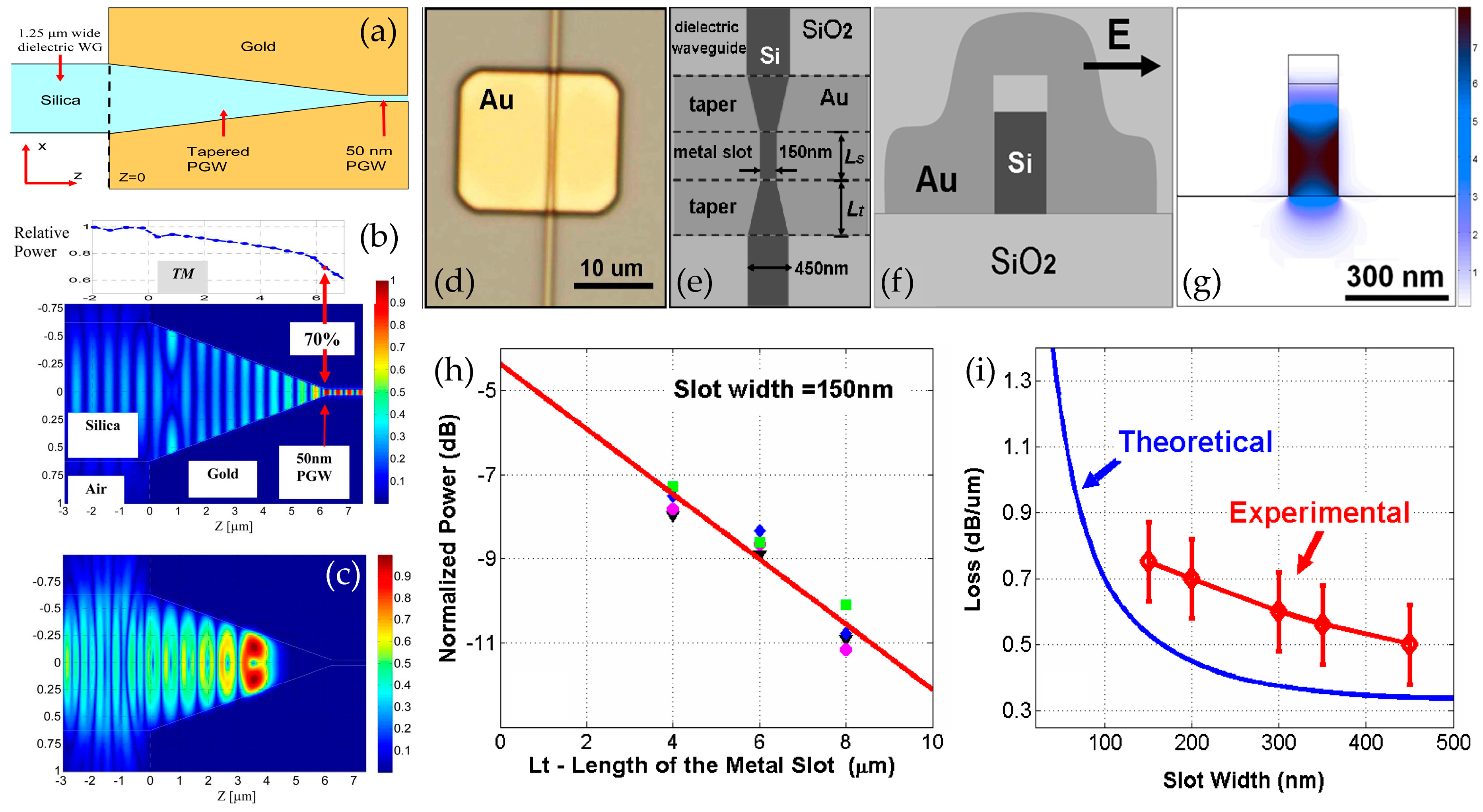
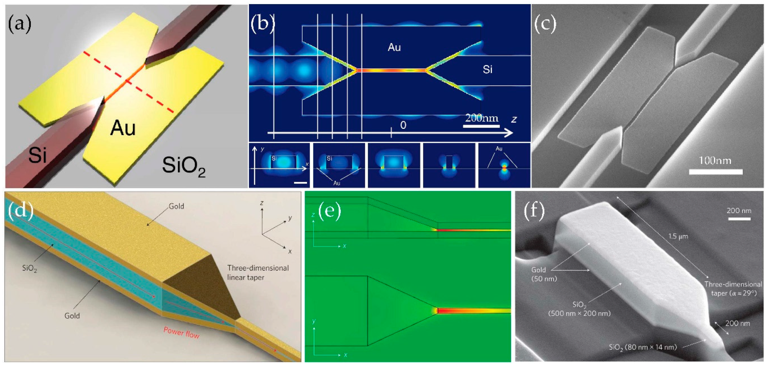
3.1. Tapered Coupling Design

Early works about the seamless transition between silicon photonic waveguides and plasmonic waveguides date back to decades ago. In 2006, Ginzburg et al. [119] theoretically demonstrated a nonadiabatic taper connecting a microscale dielectric waveguide and a nanoscale plasmonic waveguide (shown in Figure 7a). The input is a 1.25 μm-wide silica waveguide with air cladding, and the output is a 50 nm-wide gold slot with silica as the core. A 6 μm-long linear plasmonic gap taper acts as the coupler to realize mode conversion between these two types of waveguides, and a coupling loss of less than 2 dB can be achieved in theory. The field profiles simulated by FDTD are shown in Figure 7b,c. For TM excitation, the light field propagates through the taper with about 70% transmission, while for TE excitation, no plasmon mode can exist. In [120], Chen et al. fabricated metal tapers and slots on silicon-on-insulator wafers by electron-beam lithography patterning, reactive ion etching, metal evaporation, and the liftoff process. The microscope image of the fabricated sample is shown in Figure 7d, and the schematic structure is shown in Figure 7e,f. The silicon waveguide and the metal slot are both 250 nm thick, and the widths are 450 nm and 150–450 nm, respectively. The taper for coupling is about 4 μm long. Results of the experiment are shown in Figure 7h,i. From the linear fit of the normalized power versus the length of the metal slot waveguide (Figure 7h), the coupling and propagation loss for 150 nm wide metal slot can be found to be about 2.5 dB and 0.8 dB/μm, respectively.
However, if we demand stronger light confinement and higher focusing efficiency, the tapers should not only have a reduction in width but also in thickness. Figure 8 shows the reported tapered structure with a reduction in both width and thickness. Figure 8a illustrates a tapered mode converter between the Si-strip waveguide and plasmonic slot waveguide. The core size of the Si-strip waveguide is 400 nm × 200 nm, and the air-core size of the plasmonic slot waveguide is 50 nm × 20 nm. Thus, there is a large thickness mismatch between the silicon and plasmon waveguide, which should have resulted in considerable coupling loss. However, in this work [121], the authors note that the optical field in the Si-strip waveguide has two side lobes outside the core. These side lobes are similar to the mode profiles in the plasmonic slot waveguide and gradually increase in size while the light propagates to the apex of the silicon taper. Finally, they are coupled to the mode of the plasmonic slot waveguide. Due to the existence of the side lobes, a 600 nm-long tapered mode converter achieves a coupling loss of only 1.7 dB even with discontinuity in thickness. The core size of the plasmonic slot waveguide is as small as ~(λ/n)2/2000, which realizes a relatively high field intensity enhancement of 41. Furthermore, Choo et al. [122] demonstrated a three-dimensional linear taper for focusing light into an 80 nm × 14 nm MIM plasmonic waveguide (as shown in Figure 8d–f). They fabricated the 3D taper using e-beam-induced deposition (EBID), focused ion-beam (FIB) milling, and electron-beam evaporation. Without discontinuity, the 3D taper can enable the optical field to undergo a gradual conversion and achieve a field intensity enhancement of 400. Table 3 summarizes some other tapered coupling design reported in the literature.
In theory, some more complicated structures can achieve higher coupling efficiencies. For example, Veronis et al. [127] investigated a multisection tapered coupler between a 300 nm-wide Si-slab waveguide and a 50 nm-wide metal–insulator–metal plasmonic waveguides. As shown in Figure 9a, the taper consists of four silicon waveguide sections and four MIM plasmonic waveguide sections. The lengths of the eight waveguide sections are all 50 nm, and the widths of them are optimized by the microgenetic algorithm. With the optimal value of w1 = 420 nm, w2 = 440 nm, w3 = 440 nm, w4 = 340 nm, w5 = 330 nm, w6 = 40 nm, w7 = 40 nm, w8 = 120 nm, the multisection taper reaches a coupling efficiency of 93%. Similarly, a partially corrugated taper [143] (shown in Figure 9b) was demonstrated by Y. Liu. et al. The dispersion relationship of corrugated waveguides can be engineered to extend across the light line [147,148]. In the coupler design, they utilized this principle to convert the silicon-waveguide-guided mode across the light line to match the plasmonic gap waveguide mode. As a result, a coupling efficiency of 93% was also realized between a 1.25 μm-wide Si-slab waveguide and a 50 nm-wide plasmonic gap waveguide. Figure 9c illustrates a coupler structure for silicon slot waveguides and hybrid plasmonic waveguides. The coupling region consists of a small air gap with a length of Hgap = 50 nm. Compared with direct coupling, the insertion of the intermediate section improves the coupling efficiency from 75% to 90%. By taking more parameters into account, these more complicated taper structures can be designed to significantly reduce the coupling loss. However, the complexity of structures can be challenging in fabrication. In [132], a slot–funnel (SF) structure (shown in Figure 9d) for mode conversion was designed and fabricated. An additional silicon strip–slot mode converter was added before the conventional taper structure. According to the slot–slot coupling scheme, the mode and effective refractive index matching are improved, and only a small loss due to the gaps between silicon and metal is introduced. In the experiment, the coupling loss of the slot–funnel mode converter was measured to be 4 dB, which is above expectations and can be attributed to the fabrication roughness and misalignment.

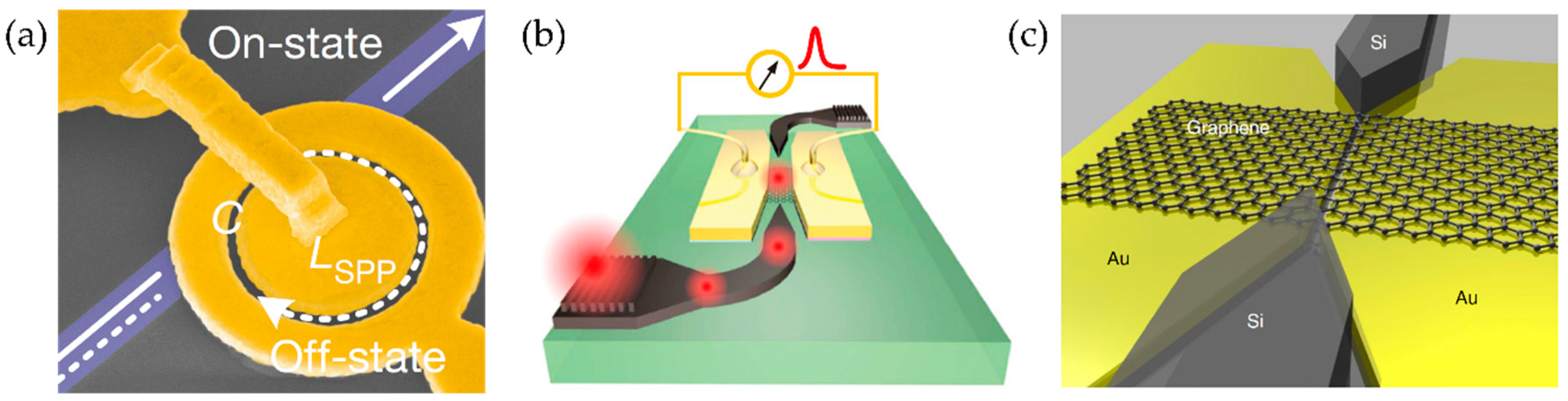
3.2. Directional Coupling Design

As opposed to tapered coupling, the silicon and plasmonic waveguides should be parallel to each other in the directional coupling design for overlapping the evanescent fields. In 2004, Hochberg et al. [149] demonstrated the directional coupling between a 500 nm × 120 nm silicon waveguide and a 100 nm-thick layer of silver. As shown in Figure 10, the silicon waveguide is placed beside the silver layer with a separation of 150 nm and a coupling length of 1.8 μm. Since the plasmonic waveguide is just a simple single interface one, the light field tends to escape into free space. The coupling loss was measured to be 4.2 ± 1.6 dB at the wavelength range of 1510–1520 nm in the experiment.
Compared with the single interface metal, the directional coupling into metal–insulator–metal multilayer plasmonic waveguides usually have better light confinement and lower coupling loss. Figure 11 shows two reported directional couplers between silicon waveguides and MIM plasmonic waveguides with horizontal and vertical space, respectively. Figure 11a,b is the cross-section and top views of a horizontally spaced directional coupler [150]. For overlapping with the evanescent fields in the silicon waveguide, the MIM plasmonic waveguide should also be a horizontally oriented one in the horizontally spaced directional coupler (as shown in Figure 11a). According to the coupled-mode theory, the TM mode couples between the silicon and plasmonic waveguides and oscillates as a function of the length. The characterization of directional coupling is illustrated in Figure 11c, in which the different coupling lengths L1 and L2 correspond to two different distances of 20 nm and 60 nm between the silicon and plasmonic waveguides. The electric field distribution is shown in Figure 11d, which also reveals the nature of field oscillating in directional coupling. In [151], Delacour et al. designed and fabricated a directional coupler with the silicon and plasmonic waveguides vertically spaced (shown in Figure 11e–i), of which the principle is the same as the previous one in [150]. In the experiment, they measured at least 70% coupling efficiency around the wavelength of 1550 nm from a 400 nm × 220 nm silicon strip waveguide to a 25 nm × 50 nm silver slot waveguide with a metal–silicon gap of 30 nm and coupling length of 0.9 μm.
The directional coupler for silicon waveguide and hybrid plasmonic waveguide was designed and fabricated by Chelladurai et al. [112] in 2019. The schematic and SEM image of the hybrid plasmonic coupler are presented in Figure 12a,b. The authors fabricated the device in three steps: first, they created the silicon by electron beam lithography and dry etching, then deposited the silica spacer layer using PECVD, and, finally, used a lift-off process to evaporate the titanium adhesion layer and the gold layer. Figure 12c shows the schematic of the structure used to measure the coupling loss and propagation loss of the coupler. By linear-fitting the measured transmission of the through and cross ports for the varying hybrid length L, the coupling loss and propagation loss could be found to be 0.16 dB/μm and 0.27 dB with the optimal structure. Compared with tapered coupling designs, the hybrid plasmonic directional coupler can achieve much higher coupling efficiency, which could be attributed to the physical principle of the directional coupling and larger fabrication tolerance of the directional coupler structure design. However, the input and output waveguides are non-collinear in the directional coupler, while the tapered coupler can simply connect the input and output waveguides together on one straight line. For these reasons, it is better to choose the coupling methods based on practical usage.

4. Prospects and Challenges of HPPs

Silicon-based hybrid plasmonic devices and circuits have attracted the interest of researchers for some time. This is due to the unique characteristics of plasmonics that can realize stronger light confinement and improve the performance and integration of silicon-based optoelectronics. Figure 13 shows some recent representative works of silicon-based hybrid plasmonics that also concern the coupling designs of plasmonic waveguides. In 2018, an outcome of a plasmonic electro-optic modulator was reported by Haffner et al. [91]. As shown in Figure 13a, the plasmonic ring resonator couples to the silicon waveguide by directional coupling methods with a coupling loss of about 1 dB. In the off state, light is coupled to the plasmonic ring resonator. While in the on state, the plasmonic ring is out of resonance to prevent coupling loss. The fabricated compact plasmonic electro-optic ring modulator can be operated at over 100 GHz with great energy efficiency. This result reveals the potential of silicon-based hybrid plasmonics to realize fast and compact communications technologies. Similarly, Ding et al. and Ono et al. demonstrated a graphene plasmonic photodetector (Figure 13b) and switch (Figure 13c), respectively, in 2020. These structures use tapered couplers to connect to silicon waveguides. Taking advantage of higher carrier mobility, unique electronic band structure, and ultra-broadband nonlinear absorption, these graphene-based devices realize ultra-compact footprints, high speed, and efficient energy consumption at the same time.
Obviously, silicon hybrid plasmonics is still in its infancy. The great dream of making hybrid plasmonic circuits on a silicon-on-insulator platform will require much further research. By using an efficient coupling design, some hybrid plasmonic components may find their way into silicon-based optoelectronics as discrete elements. However, one of the major blocks in the way is its non-compatibility with conventional CMOS fabrication processes. Involving metals or low-dimensional materials (e.g., graphene), these hybrid plasmonic components must be fabricated with film liftoff and transfer technology, which requires additional processing steps. Since silicon photonic devices are almost fully CMOS-compatible, it is our hope that some supplementary processes will be developed in the future.

5. Conclusions

In this review, we present the development trends of silicon-based optoelectronics and the challenges that can be overcome by hybrid plasmon polaritons. Silicon photonic devices and systems dissipate much less power and have greater bandwidth than electronic ones. Compatibility with the mature CMOS technology also makes silicon-based optoelectronics the best candidate for large-scale optoelectronic integration. One of the major challenges in the development of silicon-based optoelectronics is the diffraction limit, which impedes the further improvement of chip integration. Plasmonics has unique prospects for designing highly integrated optoelectronic circuits due to its significantly strong light confinement. However, metals exhibit substantial heating losses in the interaction with light. Hence, hybrid plasmon polaritons can enhance silicon-based optoelectronics in light confinement while keeping a low propagation loss. Two coupling designs for silicon and plasmonic waveguides have been reported in the literature. The tapered coupling design can achieve a higher field intensity enhancement, while the directional coupling design has a lower coupling loss. With enhancement by hybrid plasmon polaritons, it is expected that silicon-based optoelectronics will obtain further development to a higher integration scale.

Funding

This research was funded by the National Natural Science Foundation of China, grant number 61775005 and Key Program of National Natural Science Foundation of China (62035001).

Institutional Review Board Statement

Not applicable.

Informed Consent Statement

Not applicable.

Data Availability Statement

Not applicable.

Conflicts of Interest

The authors declare no conflict of interest.

References

  1. Zhou, Z.; Yin, B.; Michel, J. On-chip light sources for silicon photonics. Light Sci. Appl. 2015, 4, e358. [Google Scholar] [CrossRef]
  2. Reed, G.T.; Mashanovich, G.; Gardes, F.Y.; Thomson, D.J. Silicon optical modulators. Nat. Photonics 2010, 4, 518–526. [Google Scholar] [CrossRef] [Green Version]
  3. Liu, D.; Tang, J.; Meng, Y.; Li, W.; Zhu, N.; Li, M. Ultra-low Vpp and high-modulation-depth InP-based electro–optic microring modulator. J. Semicond. 2021, 42, 82301. [Google Scholar] [CrossRef]
  4. Dai, D.; Bowers, J.E. Silicon-based on-chip multiplexing technologies and devices for Peta-bit optical interconnects. Nanophotonics 2014, 3, 283–311. [Google Scholar] [CrossRef]
  5. Li, C.; Liu, D.; Dai, D. Multimode silicon photonics. Nanophotonics 2019, 8, 227–247. [Google Scholar] [CrossRef]
  6. Son, G.; Han, S.; Park, J.; Kwon, K.; Yu, K. High-efficiency broadband light coupling between optical fibers and photonic integrated circuits. Nanophotonics 2018, 7, 1845–1864. [Google Scholar] [CrossRef]
  7. Marchetti, R.; Lacava, C.; Carroll, L.; Gradkowski, K.; Minzioni, P. Coupling strategies for silicon photonics integrated chips [Invited]. Photonics Res. 2019, 7, 201–239. [Google Scholar] [CrossRef]
  8. Dai, D.; Bauters, J.; Bowers, J.E. Passive technologies for future large-scale photonic integrated circuits on silicon: Polarization handling, light non-reciprocity and loss reduction. Light Sci. Appl. 2012, 1, e1. [Google Scholar] [CrossRef]
  9. Su, L.; Ouyang, W.; Fang, X. Facile fabrication of heterostructure with p-BiOCl nanoflakes and n-ZnO thin film for UV photodetectors. J. Semicond. 2021, 42, 52301. [Google Scholar] [CrossRef]
  10. Yin, Z.; Hu, X.; Zeng, J.; Zeng, Y.; Peng, W. Self-powered circularly polarized light detector based on asymmetric chiral metamaterials. J. Semicond. 2020, 41, 122301. [Google Scholar] [CrossRef]
  11. Sun, C.; Wade, M.T.; Lee, Y.; Orcutt, J.S.; Alloatti, L.; Georgas, M.S.; Waterman, A.S.; Shainline, J.M.; Avizienis, R.R.; Lin, S.; et al. Single-chip microprocessor that communicates directly using light. Nature 2015, 528, 534–538. [Google Scholar] [CrossRef] [Green Version]
  12. Intel. The 50G Silicon Photonics Link; White Paper; Intel: Santa Clara, CA, USA, 2010. [Google Scholar]
  13. Vlasov, Y.A.; McNab, S.J. Losses in single-mode silicon-on-insulator strip waveguides and bends. Opt. Express 2004, 12, 1622–1631. [Google Scholar] [CrossRef]
  14. Fang, A.W.; Park, H.; Cohen, O.; Jones, R.; Paniccia, M.J.; Bowers, J.E. Electrically pumped hybrid AlGaInAs-silicon evanescent laser. Opt. Express 2006, 14, 9203–9210. [Google Scholar] [CrossRef] [PubMed]
  15. Assefa, S.; Shank, S.; Green, W.; Khater, M.; Kiewra, E.; Reinholm, C.; Vlasov, Y. A 90nm CMOS integrated Nano-Photonics technology for 25Gbps WDM optical communications applications. In Proceedings of the 2012 International Electron Devices Meeting, San Francisco, CA, USA, 10–13 December 2012; pp. 33–38. [Google Scholar]
  16. Molex Active Optical Cable. Available online: https://www.molex.com/molex/products/family (accessed on 23 August 2021).
  17. Liao, L.; Liu, A.; Rubin, D.; Basak, J.; Chetrit, Y.; Nguyen, H.; Cohen, R.; Izhaky, N.; Paniccia, M. 40 Gbit/s silicon optical modulator for high-speed applications. Electron. Lett. 2007, 43, 1196–1197. [Google Scholar] [CrossRef]
  18. Kang, Y.; Liu, H.; Morse, M.; Paniccia, M.J.; Zadka, M.; Litski, S.; Sarid, G.; Pauchard, A.; Kuo, Y.; Chen, H.; et al. Monolithic germanium/silicon avalanche photodiodes with 340 GHz gain–bandwidth product. Nat. Photonics 2009, 3, 59–63. [Google Scholar] [CrossRef]
  19. Luxtera 100G (4 × 26) PSM4 QSFP Module. Available online: http://www.luxtera.com/luxtera/products (accessed on 23 August 2021).
  20. Zhou, Z.; Chen, R.; Li, X.; Li, T. Development trends in silicon photonics for data centers. Opt. Fiber Technol. 2018, 44, 13–23. [Google Scholar] [CrossRef]
  21. International Technology Roadmap for Semiconductors 2.0, 2015 ed.; Beyond CMOS. In 2015; ITRS: New York, NY, USA, 2015.
  22. Gramotnev, D.K.; Bozhevolnyi, S.I. Plasmonics beyond the diffraction limit. Nat. Photonics 2010, 4, 83–91. [Google Scholar] [CrossRef]
  23. Barnes, W.L.; Dereux, A.; Ebbesen, T.W. Surface plasmon subwavelength optics. Nature 2003, 424, 824–830. [Google Scholar] [CrossRef]
  24. Sorger, V.J.; Oulton, R.F.; Ma, R.; Zhang, X. Toward integrated plasmonic circuits. MRS Bull. 2012, 37, 728–738. [Google Scholar] [CrossRef] [Green Version]
  25. Brongersma, M.L.; Shalaev, V.M. The Case for Plasmonics. Science 2010, 328, 440. [Google Scholar] [CrossRef]
  26. Berini, P. Figures of merit for surface plasmon waveguides. Opt. Express 2006, 14, 13030–13042. [Google Scholar] [CrossRef] [PubMed]
  27. Conway, J.A.; Sahni, S.; Szkopek, T. Plasmonic interconnects versus conventional interconnects: A comparison of latency, crosstalk and energy costs. Opt. Express 2007, 15, 4474–4484. [Google Scholar] [CrossRef]
  28. Maier, S.A. Plasmonics: Fundamentals and Applications; Springer: Berlin/Heidelberg, Germany, 2007. [Google Scholar]
  29. Bertolotti, M.; Sibilia, C.; Guzman, A.M. Evanescent Waves in Optics: An Introduction to Plasmonics; Springer: Berlin/Heidelberg, Germany, 2017; Volume 206. [Google Scholar]
  30. Ritchie, R.H. Plasma Losses by Fast Electrons in Thin Films. Phys. Rev. 1957, 106, 874–881. [Google Scholar] [CrossRef]
  31. Ozbay, E. Plasmonics: Merging Photonics and Electronics at Nanoscale Dimensions. Science 2006, 311, 189–193. [Google Scholar] [CrossRef]
  32. Khattak, H.K.; Bianucci, P.; Slepkov, A.D. Linking plasma formation in grapes to microwave resonances of aqueous dimers. Proc. Natl. Acad. Sci. USA 2019, 116, 4000. [Google Scholar] [CrossRef] [Green Version]
  33. Rotenberg, N.; Kuipers, L. Mapping nanoscale light fields. Nat. Photonics 2014, 8, 919–926. [Google Scholar] [CrossRef]
  34. Yu, H.; Peng, Y.; Yang, Y.; Li, Z. Plasmon-enhanced light–matter interactions and applications. NPJ Comput. Mater. 2019, 5, 45. [Google Scholar] [CrossRef]
  35. Wang, Y.; Plummer, E.W.; Kempa, K. Foundations of Plasmonics. Adv. Phys. 2011, 60, 799–898. [Google Scholar] [CrossRef]
  36. Enoch, S.; Bonod, N. Plasmonics: From Basics to Advanced Topics; Springer: Berlin/Heidelberg, Germany, 2012; Volume 167. [Google Scholar]
  37. Bozhevolnyi, S.I.; Martin-Moreno, L.; Garcia-Vidal, F. Quantum Plasmonics. In Springer Series in Solid-State Sciences; Springer: Berlin/Heidelberg, Germany, 2016; p. 185. [Google Scholar]
  38. Coronado, E.A.; Schatz, G.C. Surface plasmon broadening for arbitrary shape nanoparticles: A geometrical probability approach. J. Chem. Phys. 2003, 119, 3926–3934. [Google Scholar] [CrossRef]
  39. Sambles, J.R.; Bradbery, G.W.; Yang, F. Optical excitation of surface plasmons: An introduction. Contemp. Phys. 1991, 32, 173–183. [Google Scholar] [CrossRef]
  40. Beyond the diffraction limit. Nat. Photonics 2009, 3, 361. [CrossRef] [Green Version]
  41. Stockman, M.I.; Kneipp, K.; Bozhevolnyi, S.I.; Saha, S.; Dutta, A.; Ndukaife, J.; Kinsey, N.; Reddy, H.; Guler, U.; Shalaev, V.M.; et al. Roadmap on plasmonics. J. Opt. 2018, 20, 43001. [Google Scholar] [CrossRef] [Green Version]
  42. Stockman, M.I. Nanoplasmonics: The physics behind the applications. Phys. Today 2011, 64, 39–44. [Google Scholar] [CrossRef] [Green Version]
  43. Kneipp, K. Surface-enhanced Raman scattering. Phys. Today 2007, 60, 40–46. [Google Scholar] [CrossRef] [Green Version]
  44. Feng, J.; Siu, V.S.; Roelke, A.; Mehta, V.; Rhieu, S.Y.; Palmore, G.T.R.; Pacifici, D. Nanoscale Plasmonic Interferometers for Multispectral, High-Throughput Biochemical Sensing. Nano Lett. 2012, 12, 602–609. [Google Scholar] [CrossRef] [Green Version]
  45. Chung, T.; Lee, S.; Song, E.Y.; Chun, H.; Lee, B. Plasmonic Nanostructures for Nano-Scale Bio-Sensing. Sensors 2011, 11, 10907–10929. [Google Scholar] [CrossRef] [PubMed]
  46. Xu, Y.; Ji, D.; Song, H.; Zhang, N.; Hu, Y.; Anthopoulos, T.D.; Di Fabrizio, E.M.; Xiao, S.; Gan, Q. Light–Matter Interaction within Extreme Dimensions: From Nanomanufacturing to Applications. Adv. Opt. Mater. 2018, 6, 1800444. [Google Scholar] [CrossRef]
  47. Schuller, J.A.; Barnard, E.S.; Cai, W.; Jun, Y.C.; White, J.S.; Brongersma, M.L. Plasmonics for extreme light concentration and manipulation. Nat. Mater. 2010, 9, 193–204. [Google Scholar] [CrossRef]
  48. Knoll, B.; Keilmann, F. Near-field probing of vibrational absorption for chemical microscopy. Nature 1999, 399, 134–137. [Google Scholar] [CrossRef]
  49. Kawata, S.; Inouye, Y.; Verma, P. Plasmonics for near-field nano-imaging and superlensing. Nat. Photonics 2009, 3, 388–394. [Google Scholar] [CrossRef]
  50. Gramotnev, D.K.; Bozhevolnyi, S.I. Nanofocusing of electromagnetic radiation. Nat. Photonics 2014, 8, 13–22. [Google Scholar] [CrossRef]
  51. Lee, B.; Kim, S.; Kim, H.; Lim, Y. The use of plasmonics in light beaming and focusing. Prog. Quant. Electron. 2010, 34, 47–87. [Google Scholar] [CrossRef]
  52. Kim, S.; Lim, Y.; Kim, H.; Park, J.; Lee, B. Optical beam focusing by a single subwavelength metal slit surrounded by chirped dielectric surface gratings. Appl. Phys. Lett. 2008, 92, 13103. [Google Scholar] [CrossRef] [Green Version]
  53. Fu, Y.; Zhou, W.; Lim, L.E.N.; Du, C.L.; Luo, X.G. Plasmonic microzone plate: Superfocusing at visible regime. Appl. Phys. Lett. 2007, 91, 61124. [Google Scholar] [CrossRef]
  54. Mote, R.G.; Yu, S.F.; Ng, B.K.; Zhou, W.; Lau, S.P. Near-field focusing properties of zone plates in visible regime—New insights. Opt. Express 2008, 16, 9554–9564. [Google Scholar] [CrossRef]
  55. Shi, H.; Wang, C.; Du, C.; Luo, X.; Dong, X.; Gao, H. Beam manipulating by metallic nano-slits with variant widths. Opt. Express 2005, 13, 6815–6820. [Google Scholar] [CrossRef]
  56. Min, C.; Wang, P.; Jiao, X.; Deng, Y.; Ming, H. Beam focusing by metallic nano-slit array containing nonlinear material. Appl. Phys. B 2008, 90, 97–99. [Google Scholar] [CrossRef]
  57. Jia, S.; Wu, Y.; Wang, X.; Wang, N. A Subwavelength Focusing Structure Composite of Nanoscale Metallic Slits Array With Patterned Dielectric Substrate. IEEE Photonics J. 2014, 6, 1–8. [Google Scholar] [CrossRef]
  58. Wang, B.; Wu, X.; Zhang, Y. Multiple-Wavelength Focusing and Demultiplexing Plasmonic Lens Based on Asymmetric Nanoslit Arrays. Plasmonics 2013, 8, 1535–1541. [Google Scholar] [CrossRef]
  59. Meinzer, N.; Barnes, W.L.; Hooper, I.R. Plasmonic meta-atoms and metasurfaces. Nat. Photonics 2014, 8, 889–898. [Google Scholar] [CrossRef] [Green Version]
  60. Yin, L.; Vlasko-Vlasov, V.K.; Pearson, J.; Hiller, J.M.; Hua, J.; Welp, U.; Brown, D.E.; Kimball, C.W. Subwavelength Focusing and Guiding of Surface Plasmons. Nano Lett. 2005, 5, 1399–1402. [Google Scholar] [CrossRef]
  61. Nomura, W.; Ohtsu, M.; Yatsui, T. Nanodot coupler with a surface plasmon polariton condenser for optical far/near-field conversion. Appl. Phys. Lett. 2005, 86, 181108. [Google Scholar] [CrossRef]
  62. Liu, Z.; Steele, J.M.; Srituravanich, W.; Pikus, Y.; Sun, C.; Zhang, X. Focusing Surface Plasmons with a Plasmonic Lens. Nano Lett. 2005, 5, 1726–1729. [Google Scholar] [CrossRef] [PubMed]
  63. Stockman, M.I. Nanofocusing of Optical Energy in Tapered Plasmonic Waveguides. Phys. Rev. Lett. 2004, 93, 137404. [Google Scholar] [CrossRef] [PubMed] [Green Version]
  64. Babadjanyan, A.J.; Margaryan, N.L.; Nerkararyan, K.V. Superfocusing of surface polaritons in the conical structure. J. Appl. Phys. 2000, 87, 3785–3788. [Google Scholar] [CrossRef]
  65. Issa, N.A.; Guckenberger, R. Optical Nanofocusing on Tapered Metallic Waveguides. Plasmonics 2007, 2, 31–37. [Google Scholar] [CrossRef] [Green Version]
  66. Krüger, M.; Schenk, M.; Hommelhoff, P. Attosecond control of electrons emitted from a nanoscale metal tip. Nature 2011, 475, 78–81. [Google Scholar] [CrossRef] [Green Version]
  67. Nerkararyan, K.V. Superfocusing of a surface polariton in a wedge-like structure. Phys. Lett. A 1997, 237, 103–105. [Google Scholar] [CrossRef]
  68. Gramotnev, D.K.; Vernon, K.C. Adiabatic nano-focusing of plasmons by sharp metallic wedges. Appl. Phys. B 2007, 86, 7–17. [Google Scholar] [CrossRef] [Green Version]
  69. Durach, M.; Rusina, A.; Stockman, M.I.; Nelson, K. Toward Full Spatiotemporal Control on the Nanoscale. Nano Lett. 2007, 7, 3145–3149. [Google Scholar] [CrossRef] [Green Version]
  70. Vernon, K.C.; Gramotnev, D.K.; Pile, D.F.P. Adiabatic nanofocusing of plasmons by a sharp metal wedge on a dielectric substrate. J. Appl. Phys. 2007, 101, 104312. [Google Scholar] [CrossRef] [Green Version]
  71. Verhagen, E.; Kuipers, L.K.; Polman, A. Plasmonic Nanofocusing in a Dielectric Wedge. Nano Lett. 2010, 10, 3665–3669. [Google Scholar] [CrossRef] [PubMed]
  72. Gramotnev, D.K.; Tan, S.J.; Kurth, M.L. Plasmon Nanofocusing with Negative Refraction in a High-Index Dielectric Wedge. Plasmonics 2014, 9, 175–184. [Google Scholar] [CrossRef]
  73. Gramotnev, D.K. Adiabatic nanofocusing of plasmons by sharp metallic grooves: Geometrical optics approach. J. Appl. Phys. 2005, 98, 104302. [Google Scholar] [CrossRef] [Green Version]
  74. Pile, D.F.P.; Vogel, M.W.; Zhang, X.; Gramotnev, D.K. Local electric field enhancement during nanofocusing of plasmons by a tapered gap. Phys. Rev. B 2007, 75, 35431. [Google Scholar] [CrossRef] [Green Version]
  75. Gramotnev, D.K.; Vogel, M.W.; Stockman, M.I. Optimized nonadiabatic nanofocusing of plasmons by tapered metal rods. J. Appl. Phys. 2008, 104, 34311. [Google Scholar] [CrossRef] [Green Version]
  76. Pile, D.F.P.; Gramotnev, D.K. Adiabatic and nonadiabatic nanofocusing of plasmons by tapered gap plasmon waveguides. Appl. Phys. Lett. 2006, 89, 41111. [Google Scholar] [CrossRef] [Green Version]
  77. Volkov, V.S.; Bozhevolnyi, S.I.; Devaux, E.; Ebbesen, T.W. Bend loss for channel plasmon polaritons. Appl. Phys. Lett. 2006, 89, 143108. [Google Scholar] [CrossRef]
  78. Bozhevolnyi, S.I.; Volkov, V.S.; Devaux, E.; Laluet, J.; Ebbesen, T.W. Channel plasmon subwavelength waveguide components including interferometers and ring resonators. Nature 2006, 440, 508–511. [Google Scholar] [CrossRef] [PubMed]
  79. Volkov, V.S.; Bozhevolnyi, S.I.; Devaux, E.; Laluet, J.; Ebbesen, T.W. Wavelength Selective Nanophotonic Components Utilizing Channel Plasmon Polaritons. Nano Lett. 2007, 7, 880–884. [Google Scholar] [CrossRef] [PubMed]
  80. Dionne, J.A.; Sweatlock, L.A.; Sheldon, M.T.; Alivisatos, A.P.; Atwater, H.A. Silicon-Based Plasmonics for On-Chip Photonics. IEEE J. Sel. Top. Quant. 2010, 16, 295–306. [Google Scholar] [CrossRef] [Green Version]
  81. Ebbesen, T.W.; Genet, C.; Bozhevolnyi, S.I. Surface-plasmon circuitry. Phys. Today 2008, 61, 44–50. [Google Scholar] [CrossRef] [Green Version]
  82. Charbonneau, R.; Lahoud, N.; Mattiussi, G.; Berini, P. Demonstration of integrated optics elements based on long-ranging surface plasmon polaritons. Opt. Express 2005, 13, 977–984. [Google Scholar] [CrossRef]
  83. Huang, K.C.Y.; Seo, M.; Sarmiento, T.; Huo, Y.; Harris, J.S.; Brongersma, M.L. Electrically driven subwavelength optical nanocircuits. Nat. Photonics 2014, 8, 244–249. [Google Scholar] [CrossRef]
  84. Maradudin, A.A.; Novikov, I.V. Channel polaritons. Phys. Rev. B 2002, 66, 35403. [Google Scholar] [CrossRef]
  85. Gramotnev, D.K.; Pile, D.F.P. Single-mode subwavelength waveguide with channel plasmon-polaritons in triangular grooves on a metal surface. Appl. Phys. Lett. 2004, 85, 6323–6325. [Google Scholar] [CrossRef] [Green Version]
  86. Volkov, V.S.; Devaux, E.; Ebbesen, T.W.; Bozhevolnyi, S.I. Channel Plasmon-Polariton Guiding by Subwavelength Metal Grooves. Phys. Rev. Lett. 2005, 95, 46802. [Google Scholar] [CrossRef] [Green Version]
  87. Neutens, P.; Lagae, L.; Borghs, G.; Van Dorpe, P. Electrical Excitation of Confined Surface Plasmon Polaritons in Metallic Slot Waveguides. Nano Lett. 2010, 10, 1429–1432. [Google Scholar] [CrossRef]
  88. Melikyan, A.; Koehnle, K.; Lauermann, M.; Palmer, R.; Koeber, S.; Muehlbrandt, S.; Schindler, P.C.; Elder, D.L.; Wolf, S.; Heni, W.; et al. Plasmonic-organic hybrid (POH) modulators for OOK and BPSK signaling at 40 Gbit/s. Opt. Express 2015, 23, 9938–9946. [Google Scholar] [CrossRef] [Green Version]
  89. Melikyan, A.; Alloatti, L.; Muslija, A.; Hillerkuss, D.; Schindler, P.C.; Li, J.; Palmer, R.; Korn, D.; Muehlbrandt, S.; Van Thourhout, D.; et al. High-speed plasmonic phase modulators. Nat. Photonics 2014, 8, 229–233. [Google Scholar] [CrossRef]
  90. Haffner, C.; Heni, W.; Fedoryshyn, Y.; Niegemann, J.; Melikyan, A.; Elder, D.L.; Baeuerle, B.; Salamin, Y.; Josten, A.; Koch, U.; et al. All-plasmonic Mach–Zehnder modulator enabling optical high-speed communication at the microscale. Nat. Photonics 2015, 9, 525–528. [Google Scholar] [CrossRef]
  91. Haffner, C.; Chelladurai, D.; Fedoryshyn, Y.; Josten, A.; Baeuerle, B.; Heni, W.; Watanabe, T.; Cui, T.; Cheng, B.; Saha, S.; et al. Low-loss plasmon-assisted electro-optic modulator. Nature 2018, 556, 483–486. [Google Scholar] [CrossRef]
  92. Sorger, V.J.; Lanzillotti-Kimura, N.D.; Ma, R.; Zhang, X. Ultra-compact silicon nanophotonic modulator with broadband response. Nanophotonics 2012, 1, 17–22. [Google Scholar] [CrossRef] [Green Version]
  93. Dionne, J.A.; Diest, K.; Sweatlock, L.A.; Atwater, H.A. PlasMOStor: A Metal−Oxide−Si Field Effect Plasmonic Modulator. Nano Lett. 2009, 9, 897–902. [Google Scholar] [CrossRef] [PubMed]
  94. Han, Z.; Radko, I.P.; Mazurski, N.; Desiatov, B.; Beermann, J.; Albrektsen, O.; Levy, U.; Bozhevolnyi, S.I. On-Chip Detection of Radiation Guided by Dielectric-Loaded Plasmonic Waveguides. Nano Lett. 2015, 15, 476–480. [Google Scholar] [CrossRef] [Green Version]
  95. Neutens, P.; Van Dorpe, P.; De Vlaminck, I.; Lagae, L.; Borghs, G. Electrical detection of confined gap plasmons in metal–insulator–metal waveguides. Nat. Photonics 2009, 3, 283–286. [Google Scholar] [CrossRef]
  96. Falk, A.L.; Koppens, F.H.L.; Yu, C.L.; Kang, K.; de Leon Snapp, N.; Akimov, A.V.; Jo, M.; Lukin, M.D.; Park, H. Near-field electrical detection of optical plasmons and single-plasmon sources. Nat. Phys. 2009, 5, 475–479. [Google Scholar] [CrossRef]
  97. Raether, H. Surface Plasmons; Springer: Berlin/Heidelberg, Germany, 1988. [Google Scholar]
  98. Dionne, J.A.; Lezec, H.J.; Atwater, H.A. Highly Confined Photon Transport in Subwavelength Metallic Slot Waveguides. Nano Lett. 2006, 6, 1928–1932. [Google Scholar] [CrossRef]
  99. Spasenović, M.; Polman, A.; Kuipers, L.K.; Verhagen, E. Nanowire Plasmon Excitation by Adiabatic Mode Transformation. Phys. Rev. Lett. 2009, 102, 203904. [Google Scholar] [CrossRef] [Green Version]
  100. Pile, D.F.P.; Ogawa, T.; Gramotnev, D.K.; Okamoto, T.; Haraguchi, M.; Fukui, M.; Matsuo, S. Theoretical and experimental investigation of strongly localized plasmons on triangular metal wedges for subwavelength waveguiding. Appl. Phys. Lett. 2005, 87, 61106. [Google Scholar] [CrossRef] [Green Version]
  101. Steinberger, B.; Hohenau, A.; Ditlbacher, H.; Stepanov, A.L.; Drezet, A.; Aussenegg, F.R.; Leitner, A.; Krenn, J.R. Dielectric stripes on gold as surface plasmon waveguides. Appl. Phys. Lett. 2006, 88, 94104. [Google Scholar] [CrossRef]
  102. Song, Y.; Wang, J.; Li, Q.; Yan, M.; Qiu, M. Broadband coupler between silicon waveguide and hybrid plasmonic waveguide. Opt. Express 2010, 18, 13173–13179. [Google Scholar] [CrossRef]
  103. Li, Q.; Song, Y.; Zhou, G.; Su, Y.; Qiu, M. Asymmetric plasmonic-dielectric coupler with short coupling length, high extinction ratio, and low insertion loss. Opt. Lett. 2010, 35, 3153–3155. [Google Scholar] [CrossRef] [PubMed]
  104. Dai, D.; He, S. A silicon-based hybrid plasmonic waveguide with a metal cap for a nano-scale light confinement. Opt. Express 2009, 17, 16646–16653. [Google Scholar] [CrossRef] [PubMed]
  105. Sorger, V.J.; Ye, Z.; Oulton, R.F.; Wang, Y.; Bartal, G.; Yin, X.; Zhang, X. Experimental demonstration of low-loss optical waveguiding at deep sub-wavelength scales. Nat. Commun. 2011, 2, 331. [Google Scholar] [CrossRef] [Green Version]
  106. Oulton, R.F.; Sorger, V.J.; Genov, D.A.; Pile, D.F.P.; Zhang, X. A hybrid plasmonic waveguide for subwavelength confinement and long-range propagation. Nat. Photonics 2008, 2, 496–500. [Google Scholar] [CrossRef] [Green Version]
  107. Lou, F.; Dai, D.; Thylen, L.; Wosinski, L. Design and analysis of ultra-compact EO polymer modulators based on hybrid plasmonic microring resonators. Opt. Express 2013, 21, 20041–20051. [Google Scholar] [CrossRef] [PubMed]
  108. Bian, Y.; Gong, Q. Low-loss light transport at the subwavelength scale in silicon nano-slot based symmetric hybrid plasmonic waveguiding schemes. Opt. Express 2013, 21, 23907–23920. [Google Scholar] [CrossRef] [PubMed]
  109. Adhem, K.; Avrutsky, I. Local field enhancement on demand based on hybrid plasmonic-dielectric directional coupler. Opt. Express 2016, 24, 5699–5708. [Google Scholar] [CrossRef] [Green Version]
  110. Alam, M.Z.; Aitchison, J.S.; Mojahedi, M. Theoretical Analysis of Hybrid Plasmonic Waveguide. IEEE J. Sel. Top. Quant. 2013, 19, 4602008. [Google Scholar] [CrossRef]
  111. He, X.; Ning, T.; Lu, S.; Zheng, J.; Li, J.; Li, R.; Pei, L. Ultralow loss graphene-based hybrid plasmonic waveguide with deep-subwavelength confinement. Opt. Express 2018, 26, 10109–10118. [Google Scholar] [CrossRef] [PubMed]
  112. Chelladurai, D.; Doderer, M.; Koch, U.; Fedoryshyn, Y.; Haffner, C.; Leuthold, J. Low-loss hybrid plasmonic coupler. Opt. Express 2019, 27, 11862–11868. [Google Scholar] [CrossRef] [PubMed]
  113. Prodan, E.; Radloff, C.; Halas, N.J.; Nordlander, P. A Hybridization Model for the Plasmon Response of Complex Nanostructures. Science 2003, 302, 419. [Google Scholar] [CrossRef]
  114. Haus, H.A.; Huang, W. Coupled-mode theory. Proc. IEEE 1991, 79, 1505–1518. [Google Scholar] [CrossRef] [Green Version]
  115. Nishihara, H.; Haruna, M.; Suhara, T. Optical Integrated Circuits; McGraw Hill Professional: New York, NY, USA, 1989; Volume 1. [Google Scholar]
  116. Hardy, A.; Streifer, W. Coupled mode theory of parallel waveguides. J. Lightwave Technol. 1985, 3, 1135–1146. [Google Scholar] [CrossRef]
  117. Breukelaar, I.G. Surface Plasmon-Polaritons in Thin Metal Strips and Slabs: Waveguiding and Mode Cutoff. Ph.D. Thesis, University of Ottawa, Ottawa, ON, Canada, 2004. [Google Scholar]
  118. Shahbazyan, T.V.; Stockman, M.I. Plasmonics: Theory and Applications; Springer: Berlin/Heidelberg, Germany, 2013. [Google Scholar]
  119. Ginzburg, P.; Arbel, D.; Orenstein, M. Gap plasmon polariton structure for very efficient microscale-to-nanoscale interfacing. Opt. Lett. 2006, 31, 3288–3290. [Google Scholar] [CrossRef] [PubMed] [Green Version]
  120. Chen, L.; Shakya, J.; Lipson, M. Subwavelength confinement in an integrated metal slot waveguide on silicon. Opt. Lett. 2006, 31, 2133–2135. [Google Scholar] [CrossRef]
  121. Ono, M.; Taniyama, H.; Xu, H.; Tsunekawa, M.; Kuramochi, E.; Nozaki, K.; Notomi, M. Deep-subwavelength plasmonic mode converter with large size reduction for Si-wire waveguide. Optica 2016, 3, 999–1005. [Google Scholar] [CrossRef]
  122. Choo, H.; Kim, M.; Staffaroni, M.; Seok, T.J.; Bokor, J.; Cabrini, S.; Schuck, P.J.; Wu, M.C.; Yablonovitch, E. Nanofocusing in a metal–insulator–metal gap plasmon waveguide with a three-dimensional linear taper. Nat. Photonics 2012, 6, 838–844. [Google Scholar] [CrossRef] [Green Version]
  123. Zhu, K.; Xu, P.; Sun, P.; Liu, X.; Li, H.; Zhou, Z. An Ultra-compact Broadband TE-pass Nanofocusing Structure. In Proceedings of the Asia Communications and Photonics Conference/International Conference on Information Photonics and Optical Communications 2020 (ACP/IPOC), Beijing, China, 24–27 October 2020; p. M151A. [Google Scholar]
  124. Zhu, K.; Xu, P.; Sun, P.; Liu, X.; Li, H.; Zhou, Z. Low Loss, High Extinction Ratio Plasmonic Spot Size Converter. In Proceedings of the Asia Communications and Photonics Conference/International Conference on Information Photonics and Optical Communications 2020 (ACP/IPOC), Beijing, China, 24–27 October 2020; p. M31A. [Google Scholar]
  125. Tian, J.; Yu, S.; Yan, W.; Qiu, M. Broadband high-efficiency surface-plasmon-polariton coupler with silicon-metal interface. Appl. Phys. Lett. 2009, 95, 13504. [Google Scholar] [CrossRef]
  126. Han, Z.; Elezzabi, A.Y.; Van, V. Experimental realization of subwavelength plasmonic slot waveguides on a silicon platform. Opt. Lett. 2010, 35, 502–504. [Google Scholar] [CrossRef]
  127. Veronis, G.; Fan, S. Theoretical investigation of compact couplers between dielectric slab waveguides and two-dimensional metal-dielectric-metal plasmonic waveguides. Opt. Express 2007, 15, 1211–1221. [Google Scholar] [CrossRef] [PubMed] [Green Version]
  128. Briggs, R.M.; Grandidier, J.; Burgos, S.P.; Feigenbaum, E.; Atwater, H.A. Efficient Coupling between Dielectric-Loaded Plasmonic and Silicon Photonic Waveguides. Nano Lett. 2010, 10, 4851–4857. [Google Scholar] [CrossRef] [PubMed] [Green Version]
  129. Conway, J. Efficient Optical Coupling to the Nanoscale. Ph.D. Thesis, University of California, Los Angeles, CA, USA, 2006. [Google Scholar]
  130. Yu, J.; Ohtera, Y.; Yamada, H. Highly efficient coupler for dielectric slot waveguides and hybrid plasmonic waveguides. Jpn. J. Appl. Phys. 2018, 57, 052202. [Google Scholar] [CrossRef]
  131. Chen, C.T.; Xu, X.; Hosseini, A.; Pan, Z.; Subbaraman, H.; Zhang, X.; Chen, R.T. Design of Highly Efficient Hybrid Si-Au Taper for Dielectric Strip Waveguide to Plasmonic Slot Waveguide Mode Converter. J. Lightwave Technol. 2015, 33, 535–540. [Google Scholar] [CrossRef]
  132. Zhu, B.Q.; Tsang, H.K. High Coupling Efficiency Silicon Waveguide to Metal–Insulator–Metal Waveguide Mode Converter. J. Lightwave Technol. 2016, 34, 2467–2472. [Google Scholar] [CrossRef]
  133. Feng, N.; Dal Negro, L. Plasmon mode transformation in modulated-index metal-dielectric slot waveguides. Opt. Lett. 2007, 32, 3086–3088. [Google Scholar] [CrossRef] [Green Version]
  134. Zhu, S.; Liow, T.Y.; Lo, G.Q.; Kwong, D.L. Silicon-based horizontal nanoplasmonic slot waveguides for on-chip integration. Opt. Express 2011, 19, 8888–8902. [Google Scholar] [CrossRef]
  135. Ginzburg, P.; Arbel, D.; Tein, M.O. Efficient Coupling of Nano-Plasmonics to Micro-Photonic Circuitry. In Proceedings of the Conference on Lasers and Electro-Optics/Quantum Electronics and Laser Science and Photonic Applications Systems Technologies, Baltimore, MD, USA, 22–27 May 2005; p. N5. [Google Scholar]
  136. Ginzburg, P.; Arbel, D.; Orenstein, M. Surface Plasmon Assisted Interfacing between Nano and Micro Scale Photonic Circuits. In Proceedings of the Integrated Photonics Research and Applications/Nanophotonics for Information Systems, San Diego, CA, USA, 10–13 April 2005; p. A5. [Google Scholar]
  137. Yang, R.; Wahsheh, R.A.; Lu, Z.; Abushagur, M.A.G. Efficient light coupling between dielectric slot waveguide and plasmonic slot waveguide. Opt. Lett. 2010, 35, 649–651. [Google Scholar] [CrossRef]
  138. Wu, M.; Han, Z.; Van, V. Conductor-gap-silicon plasmonic waveguides and passive components at subwavelength scale. Opt. Express 2010, 18, 11728–11736. [Google Scholar] [CrossRef]
  139. Lau, B.; Swillam, M.A.; Helmy, A.S. Hybrid orthogonal junctions: Wideband plasmonic slot-silicon waveguide couplers. Opt. Express 2010, 18, 27048–27059. [Google Scholar] [CrossRef]
  140. Shi, P.; Zhou, G.; Chau, F.S. Enhanced coupling efficiency between dielectric and hybrid plasmonic waveguides. J. Opt. Soc. Am. B 2013, 30, 1426–1431. [Google Scholar] [CrossRef]
  141. Lee, S.; Park, J.; Kang, M.; Lee, B. Highly efficient plasmonic interconnector based on the asymmetric junction between metal-dielectric-metal and dielectric slab waveguides. Opt. Express 2011, 19, 9562–9574. [Google Scholar] [CrossRef]
  142. Heydari, M.B.; Asgari, M.; Jafari, N. Novel analytical model for nano-coupler between metal–insulator–metal plasmonic and dielectric slab waveguides. Opt. Quant. Electron. 2018, 50, 432. [Google Scholar] [CrossRef]
  143. Liu, Y.; Lai, Y.; Chang, K. Plasmonic Coupler for Silicon-Based Micro-Slabs to Plasominc Nano-Gap Waveguide Mode Coversion Enhancement. J. Lightwave Technol. 2013, 31, 1708–1712. [Google Scholar] [CrossRef]
  144. Lim, H.J.; Kwon, M.S. Efficient Coupling Between Photonic and Dielectric-Loaded Surface Plasmon Polariton Waveguides with the Same Core Material. IEEE Photonics J. 2014, 6, 1–9. [Google Scholar] [CrossRef] [Green Version]
  145. Desiatov, B.; Goykhman, I.; Levy, U. Plasmonic nanofocusing of light in an integrated silicon photonics platform. Opt. Express 2011, 19, 13150–13157. [Google Scholar] [CrossRef]
  146. Wahsheh, R.A.; Abushagur, M.A.G. Experimental and theoretical investigations of an air-slot coupler between dielectric and plasmonic waveguides. Opt. Express 2016, 24, 8237–8242. [Google Scholar] [CrossRef] [PubMed]
  147. Brimont, A.; Vicente Galán, J.; Maria Escalante, J.; Martí, J.; Sanchis, P. Group-index engineering in silicon corrugated waveguides. Opt. Lett. 2010, 35, 2708–2710. [Google Scholar] [CrossRef]
  148. Bryant, G.H. Propagation in Corrugated Waveguides. Proc. Inst. Electr. Eng. 1969, 116, 203–213. [Google Scholar] [CrossRef]
  149. Hochberg, M.; Baehr-Jones, T.; Walker, C.; Scherer, A. Integrated plasmon and dielectric waveguides. Opt. Express 2004, 12, 5481–5486. [Google Scholar] [CrossRef] [PubMed] [Green Version]
  150. Melikyan, A.; Kohl, M.; Sommer, M.; Koos, C.; Freude, W.; Leuthold, J. Photonic-to-plasmonic mode converter. Opt. Lett. 2014, 39, 3488–3491. [Google Scholar] [CrossRef] [PubMed]
  151. Delacour, C.; Blaize, S.; Grosse, P.; Fedeli, J.M.; Bruyant, A.; Salas-Montiel, R.; Lerondel, G.; Chelnokov, A. Efficient Directional Coupling between Silicon and Copper Plasmonic Nanoslot Waveguides: Toward Metal−Oxide−Silicon Nanophotonics. Nano Lett. 2010, 10, 2922–2926. [Google Scholar] [CrossRef]
  152. Ding, Y.; Cheng, Z.; Zhu, X.; Yvind, K.; Dong, J.; Galili, M.; Hu, H.; Mortensen, N.A.; Xiao, S.; Oxenløwe, L.K. Ultra-compact integrated graphene plasmonic photodetector with bandwidth above 110 GHz. Nanophotonics 2020, 9, 317–325. [Google Scholar] [CrossRef] [Green Version]
  153. Ono, M.; Hata, M.; Tsunekawa, M.; Nozaki, K.; Sumikura, H.; Chiba, H.; Notomi, M. Ultrafast and energy-efficient all-optical switching with graphene-loaded deep-subwavelength plasmonic waveguides. Nat. Photonics 2020, 14, 37–43. [Google Scholar] [CrossRef] [Green Version]
Figure 1. The development trend of silicon-based optoelectronics and some significant works in the past few decades. Figures reproduced from [11,12,13,14,15,16].
Photonics 08 00482 g001
Figure 2. (a) Optical field profile (Ez) of surface plasmons on the air–Ag interface. (b) The operating speed and device sizes of semiconductor electronics, dielectric photonics, and plasmonics. Plasmonics can bridge the gap between nanoelectronics and photonics.
Photonics 08 00482 g002
Figure 3. The unique dispersion curve of surface plasmons mode illustrates the momentum mismatch, with the surface plasmons mode lying on the right side of the light line. This yields extraordinary high wave vectors k sp capable of overcoming the diffraction limit of light.
Photonics 08 00482 g003
Figure 4. Topographical (a,c,e,g,i,l) and near-field optical (b,d,f,h,j,k,m) images of plasmonic subwavelength waveguide components. (a,b) S-bend [77]. (c,d) Y-splitter [77]. (e,f) Mach–Zehnder (M.Z.) interferometer [78]. (g,h) Waveguide–ring (WR) resonator [78]. (ik) WR-resonator-based add-drop multiplexer [79]. (l,m) Bragg grating filter (BGF) [79]. Figures reproduced from (ad) [77]; (eh) [78]; (im) [79].
Photonics 08 00482 g004
Figure 5. Schematics (a,c) and field distributions (b,d) of two types of hybrid plasmonic waveguides reported in literature. (a,b) A dielectric cylinder above a metal surface [106]. (c,d) A metal cap on an SOI slab with a low-index nano-layer between them [104]. This type of hybrid plasmonic waveguide is compatible with standard processes for SOI wafers and is thus easily fabricated. Figures reproduced from (b) [106]; (d) [104].
Photonics 08 00482 g005
Figure 6. Schematics illustrating the light confinement of (a) dielectric versus (b) plasmonic waveguides for various core diameters. The dotted lines approximately indicate the 1/e level of the field.
Photonics 08 00482 g006
Figure 7. Tapered coupling design with reduction in width. Schematic configuration of the proposed taper for coupling a 1.25 μm-wide dielectric strip waveguide with a 50 nm-wide metal slot waveguide (a) and its field profile (b,c) [119]. Microscope image (d), schematic structure (e,f), and field distribution (g) of the fabricated tapered coupler between a standard silicon strip waveguide and a metal slot waveguide. (h,i) The transmitted power as a function of the length of metal slot Lt and the propagation losses as a function of the metal slot width, respectively [120]. The wavelength λ = 1550 nm. Figures reproduced from (ac) [119]; (di) [120].
Photonics 08 00482 g007
Figure 8. Tapered coupling design with reduction in both width and thickness. (ac) A taper with large reduction in thickness for Si-strip waveguide to plasmonic slot waveguide mode conversion [121]. (df) A three-dimensional linear taper for highly efficient nanofocusing in MIM plasmonic waveguide [122]. (a,d) Schematics of the proposed tapers. (b,e) Field distributions. (c,f) SEM images of the fabricated tapers. Figures reproduced from (ac) [121]; (df) [122].
Photonics 08 00482 g008
Figure 9. Some more complicated tapered coupling designs with simulated coupling efficiencies of (a) 93% [127], (b) 93% [143], (c) 90% [130], and experimentally measured coupling loss of (d) 4 dB [132]. Figures reproduced from (a) [127]; (b) [143]; (c) [130]; (d) [132].
Photonics 08 00482 g009
Figure 10. Directional coupling between silicon waveguides and a single interface plasmonic waveguide. (a) A rendering of simulated field profile of the coupler. (b) An SEM image of the fabricated coupler. Figures reproduced from [149].
Photonics 08 00482 g010
Figure 11. Directional coupling between silicon waveguides and metal–insulator–metal plasmonic waveguides. (a) Cross-section and (b) top views of a horizontally spaced directional coupler, of which the coupling efficiency and field distribution are shown in (c,d), respectively. (e) Perspective and (f) side views of a vertically spaced directional coupler, of which the SEM cross-section view, top view, and normalized transmission are shown in (g,h,i), respectively. Figures reproduced from (ad) [150]; (ei) [151].
Photonics 08 00482 g011
Figure 12. Directional coupling between silicon waveguides and hybrid plasmonic waveguides. (a) Schematic structure and (b) SEM image of the proposed coupler. (c) Schematic structure used to measure the coupling efficiency in the experiment. (d) Measured (dots) and simulated (solid lines) coupling efficiencies as functions of the gap width. Figures reproduced from [112].
Photonics 08 00482 g012
Figure 13. Some latest works of HPPs based on SOI platform. (a) A plasmonic electro-optic modulator. (b) An integrated graphene plasmonic photodetector. (c) A graphene-loaded plasmonic all-optical switch. Figures reproduced from (a) [91]; (b) [152]; (c) [153].
Photonics 08 00482 g013
Table 1. The properties of metal for different frequency of light.
Frequency
region
Very high
frequency
Optical
frequency
Very low
frequency
At plasma frequency
Photonics 08 00482 i001 Photonics 08 00482 i002 ε ( ω ) = 1 ω p 2 ω 2 + i γ ω is complex Photonics 08 00482 i003
ω > ω p γ ω < ω p ω γ ω = ω p
Relative permittivity ε > 0 ,   ε 0 ε < 0 ,   ε 0 ε ε ε 0
Refractive index n > 0 ,   n 0
n is real
n 0 ,   n > 0
n is complex
n n ε / 2 n 0
Properties of Metal Photonics 08 00482 i004
Metal is like dielectric
Photonics 08 00482 i005
Fields decay exponentially
Photonics 08 00482 i006
Fields decay rapidly
Only collective longitudinal oscillations of free electrons exist (called volume plasmons)
Table 2. Attenuation of several types of plasmonic waveguides reported in literature by experiments.
Waveguide TypeSchematics 1Free Space Wavelength λ (nm) M o d e   A r e a ( λ / 2 ) 2 Propagation   Length   L m / λ
Metal–insulator–metal (MIM) [98] Photonics 08 00482 i00768510%5
Insulator–metal–insulator (IMI) [99] Photonics 08 00482 i008155014%14
Triangular metal wedge [100] Photonics 08 00482 i009633-2
Dielectric stripe on metal [101] Photonics 08 00482 i010800-10
1 The schematics show the plasmonic waveguide cross-sections, with the optical field propagating in the third dimension. The yellow color marks metal, blue—dielectric, pink—mode intensity distributions.
Table 3. Summary of reported taper design for coupling silicon waveguides with plasmonic waveguides.
Ref.Dielectric Waveguide
Type and Core Size
Plasmonic Waveguide
Type and Core Size
Taper Length
/nm
λ/nmCoupling Loss/dBPropagation Loss
/(dB × μm −1)
Field
Enhancement
[123]Si-strip 400 nm × 220 nmHPW 60 nm × 20 nm10801550<0.8-135.5
[124]Si-strip 400 nm × 220 nmHPW 20 nm × 40 nm-1550<0.7-75
[102]Si-strip 450 nm × 250 nmHPW 200 nm × 250 nm40015501.5--
[121] *Si-strip 400 nm × 200 nmAu-air-Au 50 nm × 20 nm6001500–16001.71.841
[125] *Si-strip 450 nm × 250 nmAu-air-Au 200 nm × 250 nm958.91460–15404.52.5-
[122] *SiO2-strip 500 nm × 200 nmAu- SiO2-Au 80 nm × 14 nm15008301.34.9400
[126] *Si-strip 300 nm × 340 nmAu-PMMA-Au 200 nm × 200 nm>250015505.20.78-
[119]SiO2-strip 1250 nm in widthAu- SiO2-Au 50 nm in width600015501.5--
[127]Si-strip 300 nm in widthAg-air-Ag 50 nm in width40015500.3--
[128] *Si-ridge 740 nm × 220 nmDielectric-loaded 500 nm × 560 nm~2000155010.09-
[129]SiO2-slab 50 nm in thicknessAg- SiO2-Ag 1 nm in thickness~428476~2~109~350
[130]Si-slot 650 nm in widthHPW 300 nm in width501550~0.5--
[131]Si-strip 450 nm × 250 nmAu-SU8-Au 250 nm × 250 nm170015500.30.32-
[132] *Si-strip 450 nm × 230 nmAu-PMMA-Au 80 nm × 180 nm5400164041.8-
[133]Si-strip 450 nm × 300 nmHPW 350 nm × 300 nm5001400–1700<0.10.116
[120] *Si-strip 450 nm × 250 nmAu-Si-Au 150 nm × 250 nm400015502.50.8-
[134] *Si-strip 500 nm × 340 nmHPW 45 nm × 340 nm100015500.40.63-
[135]SiO2-strip 1250 nm in widthAu- SiO2-Au 50 nm in width250015501.5--
[136]SiO2-strip 1250 nm in widthAu- SiO2-Au 50 nm in width60001550<2--
[137] *Si-slot 460 nm × 260 nmAu-air-Au 80 nm × 260 nm-15503.72-
[138] *Si-strip 1000 nm × 340 nmHPW 200 nm × 440 nm100015500.970.1-
[139] *Si-strip 400 nm × 340 nmAg-air-Ag 50 nm × 340 nm-1530–1590~1.5~3.6-
[140]Si-strip with SiN 400 nm × 390 nmHPW 200 nm × 460 nm3001300–1650<0.5~0.2-
[141]Si-strip 1000 nm × 370 nmAg- SiO2-Ag 1000 nm × 100 nm5401550~0.6--
[142]Si-slab 300 nm in widthAg-air-Ag 63 nm in width-15501.2--
[143]Si-slab 1250 nm in widthAg-Si-Ag 50 nm in width150015500.3--
[144] *Si-strip 2500 nm × 900 nmHPW 500 nm × 900 nm400015501.10.083-
[145] *Si-strip 900 nm × 250 nmAu-Si-Au 50 nm × 200 nm20001552~1.2-~10
[146] *Si-strip 460 nm × 250 nmAu-air-Au 80 nm × 250 nm501260–1620~2.8~2-
* Experimental results.
Publisher’s Note: MDPI stays neutral with regard to jurisdictional claims in published maps and institutional affiliations.

