Article

An Ultra-Compact Design of Plasmonic Memristor with Low Loss and High Extinction Efficiency Based on Enhanced Interaction between Filament and Concentrated Plasmon

1
School of Information and Electronic Engineering, Hunan City University, Yiyang 413000, China
2
Chongqing United Microelectronics Center, Chongqing 410332, China
3
All-Solid-State Energy Storage Materials and Devices Key Laboratory of Hunan Province, Yiyang 413000, China
*
Author to whom correspondence should be addressed.
Photonics 2021, 8(10), 437; https://doi.org/10.3390/photonics8100437
Submission received: 4 September 2021 / Revised: 2 October 2021 / Accepted: 7 October 2021 / Published: 12 October 2021

Abstract

:
We present a numerical design of the plasmonic memristive switching device operated at the telecommunication wavelength of 1.55 μm, which consists of a triangle-shaped metal taper mounted on top of a Si waveguide, with rational doping in the area below the apex of the taper. This device can achieve optimal vertical coupling of light energy from the Si waveguide to the plasmonic region and, at the same time, focus the plasmon into the apex of the metal taper. Moreover, the area with concentrated plasmon is overlapped with that where the memristive switching occurs, due to the formation/removal of the metallic nano-filament. As a result, the highly distinct transmission induced by the switching of the plasmonic memristor can be produced because of the maximized interactions between the filament and the plasmon. Our numerical simulation shows that the device hasa compact size (610 nm), low insertion loss (~1 dB), and high extinction efficiency (4.6 dB/μm). Additionally, we point out that stabilizing the size of the filament is critical to improve the operation repeatability of the plasmonic memristive switching device.

1. Introduction

Integrated photonic chips have been widely studied and applied in photonic science and engineering, which can efficiently speed up on-chip information processing [1]. However, owing to the diffraction limit, it is difficult to realize integrated photonic circuits with a density comparable to the electronic counterpart [1]. In recent years, much research attention has been paid to plasmonic devices, which have the capability of controlling the light fieldon a deep subwavelength scale [2,3,4,5,6]. Along with the good development of the components for the propagation, modulationand detection of plasmon [7,8,9], explorations of plasmonic devices for logic operation and data storage are also on the road, e.g., recently, surface plasmon polaritons (SPP) were introduced into the memristor, making its resistive state optical readable [10]. This is from the perspective that the combination of plasmon and the memristor might induce unique opportunities for new functional plasmonic devices.
The memristor is a device that can be tuned between a high-resistance (HR) state and low-resistance (LR) state by the external voltage/current signal (Figure 1a) [11]. It typically consists of a capacitor-like metal–insulator–metal (MIM) or metal–insulator–semiconductor (MIS) structure [11,12,13], which naturallycould also serve as the plasmonic waveguide [14]. Hence, interestingly, the memristor in an HR or LR state could exhibit a discrepant optical response when interacting with the plasmon, as shown in Figure 1b [10,14,15]. This system (namely, “plasmonic memristor”), on one hand, has volatile or non-volatile memory with electrical write/erase and optical readout functionality [10,15,16]. On the other hand, noting the potential of the memristor as a basic unit for a chip with the capability of neuron computation and implication logical operation [17,18], many of the applications, such as in-memory optical computing, optoelectronic artificial synapses, image recognition and even neuromorphic visual systems, were explored at different wavelength ranges [10,14,15,19,20,21,22,23]. The plasmonic memristor based on a silicon photonics platform is especially attractive, due to its emerging chances to realize large-scale interrogation via a CMOS compatible process [10,14,15,19,20], as well as its potential to fuse its data processing capability with the strong power of silicon photonics on data transmission at communication wavelengths around 1.31 μm and 1.55 μm [19,20].
There are many memristive mechanisms [24,25,26], which enable the use of optical memristive switches at the micro- to atomic scale [16]. In the plasmonic memristor based on the formation/rupture of the metallic filament in the insulator, its filament induces absorption and scattering in small volumes at the nano- or even atomic scale [10,14].This, in principle, is quite beneficial to shrink the size of the plasmonic memristor. In this work, we numerically design a plasmonic memristor operating at a telecom wavelength of 1.55 μm, based on filament formation/rupture. The simulation shows that the proposed structure is rather compact (width ~400 nm, length ~610 nm), and with a relative low loss and high extinction efficiency [10,14].

2. Experimental and Methods

The basic structure of the device proposed in this work is a small triangle-shaped Ag taper on top of a silicon (Si) waveguide, as shown in Figure 1c. The substrate is silicon dioxide (SiO2), and a SiO2 buffer layer is used to separate the Ag triangle and the Si waveguide. Such an MIS (Ag/SiO2/Si) structure could guide the plasmon, but to ensure the device could truly work similarly to a plasmonic memristor, we still experimentally pre-check the memristive behaviors of the Ag/SiO2/Si tri-layered system. Its preparation starts from the p-doped Si substrate, which is ultrasonically cleaned successively in acetone, ethanol, acetone, ethanol, and deionized water for 10 min each, then blown dry by N2 flow and baked in vacuum oven at 120 °C for 2 h. A layer ofSiO2 with thickness of ~30 nm is deposited by e-beam evaporation (BOC Edward FL400) on the cleaned silicon chip, which is dipped in 10% HF solution and blown dry by N2 flow to remove the natural surface oxide layer. After that, the top electrode Ag layer with 100 nm thickness is defined by lithography plus lift-off process (SUSS MJB4). The electrical tests on the obtained sample are performed on Keithley-2635A sourcemeter. A voltage sequence (0 V → 2 V → −1 V → 0 V) is applied on the Ag/SiO2/Si trilayer structure and the current is probed, where the positive voltage is applied from Ag to Si (serves as the grounded bottom electrode). On the other hand, the numerical design of the plasmonic memristor containingAg/SiO2/Si trilayer structure is performed in FDTD solution and mode solution from Ansys-Lumerical.

3. Results and Discussions

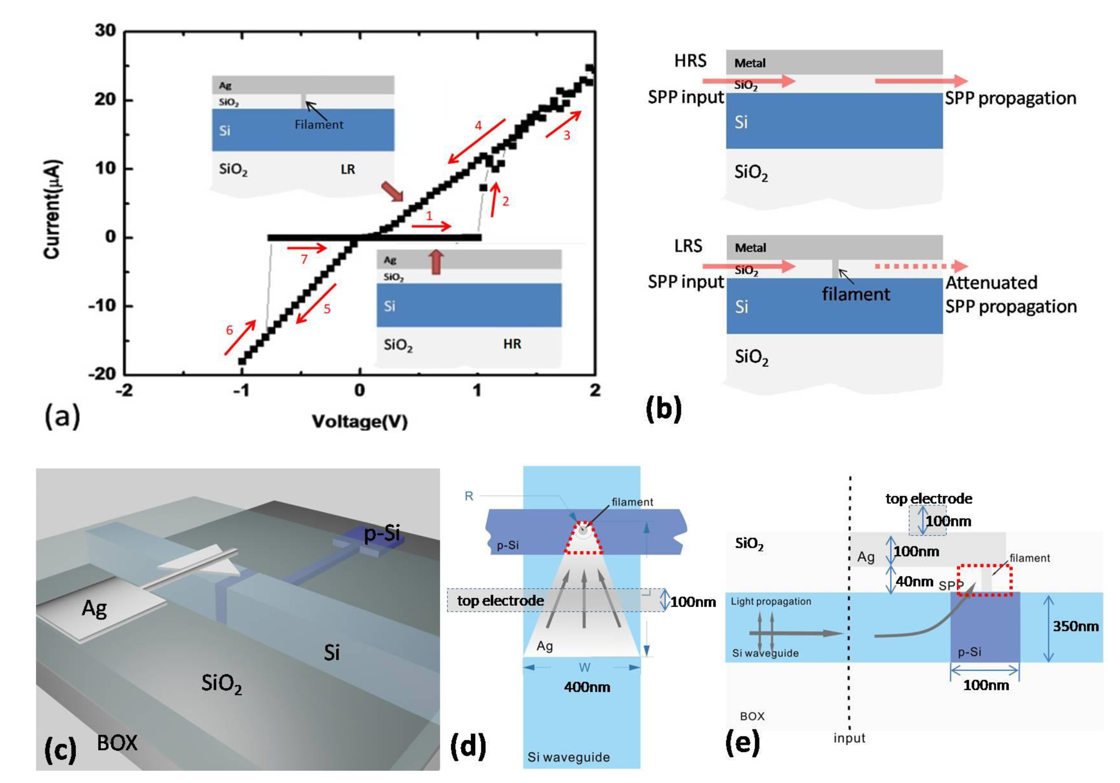
3.1. The Device Working Principle

As shown in Figure 1a, as the positive voltage reaches ~1 V, the current through the device presents a sudden increase, which corresponds to the switching of the Ag/SiO2/Si system from an HR to LR state; while, in the negative voltage regime, a voltage ~−0.8 V could produce the reverse switching from the LR to HR state. Such inter-switching between the HR and LR state, under a rational electrical field, is a typical memristive phenomenon, verifying the Ag/SiO2/Si trilayer structure could be a good memristor. Moreover, the IV characteristic of the Ag/SiO2/Si device in the LR state seems highly ohmic, which is a conductive feature of the metal and strongly implies the formation of a metal filament during the switching. Hence, without the loss of rationality, we assume that the Ag/SiO2/Si memristor is based on a metal filament formation/rupture mechanism. Under this precondition, the Ag/SiO2/Si system with a triangle-shaped Ag taperis employed to design the plasmonic memristor because it is a memristor and could simultaneously support the HP mode in the SiO2 buffer layer.
In this system, it has been observed that the plasmon can be concentrated to the area below the apex of the taper (Figure 1d, the top view of the structure), while the loss is low and the size is small [27,28]. Hence, if the length of the taper is also chosen to maximize the energy transfer from the incident Si waveguide to plasmonic taper (Figure 1e, the side view of the structure) [28], these two factors together ensure that the electromagnetic energy of the incident light could be tightly focused on the SiO2 buffer layer at the area below the apex of the taper, with a small volume. Furthermore, the Ag taper can also be employed as the top electrode of the plasmonic memristor, and connected via the Ag line on its upper side, while the bottom electrode is the silicon with p-doping in the area below the apex of the taper (note that the Ag taper, the SiO2 buffer layer, and the Si waveguide together form the memristive Ag/SiO2/Si trilayer structure; the heavy doping level to the silicon at the ~1020 cm3 level is suggested to minimize series resistance [29]). Since the memristive behavior (the filament forms or dissolves) would just take place in the area sandwiched by the top and bottom electrode [24,26], i.e., the zone in the SiO2 buffer layer below the apex of the taper (as marked by a red dotted line in Figure 1d,e), the memristive area would be exactly overlapped with the concentrated light. As a result, the interactions between the plasmon and the filament are maximized to obtain a high extinction efficiency. Meanwhile, the device has a compact size (as discussed below), and, consequently, low loss. This is the core thought of our work.
The geometric structure of the device is shown in its top view (Figure 1d) and side view (Figure 1e). We use W to denote the length of the base of the isosceles triangle (metal taper), and L to denote the perpendicular length from the input side to the apex. For simplicity, we will call W the (maximum) width of the triangle and L the length of the triangle throughout this paper. Since the apex of the metal triangle is always rounded up in real manufacturing, we introduce the radius of curvature R (=20 nm) at the tip, which is a typical feature size feasible by, e.g., a regular e-beam lithography tool, if no special measures are conducted to further enhance the fabrication resolution [30].

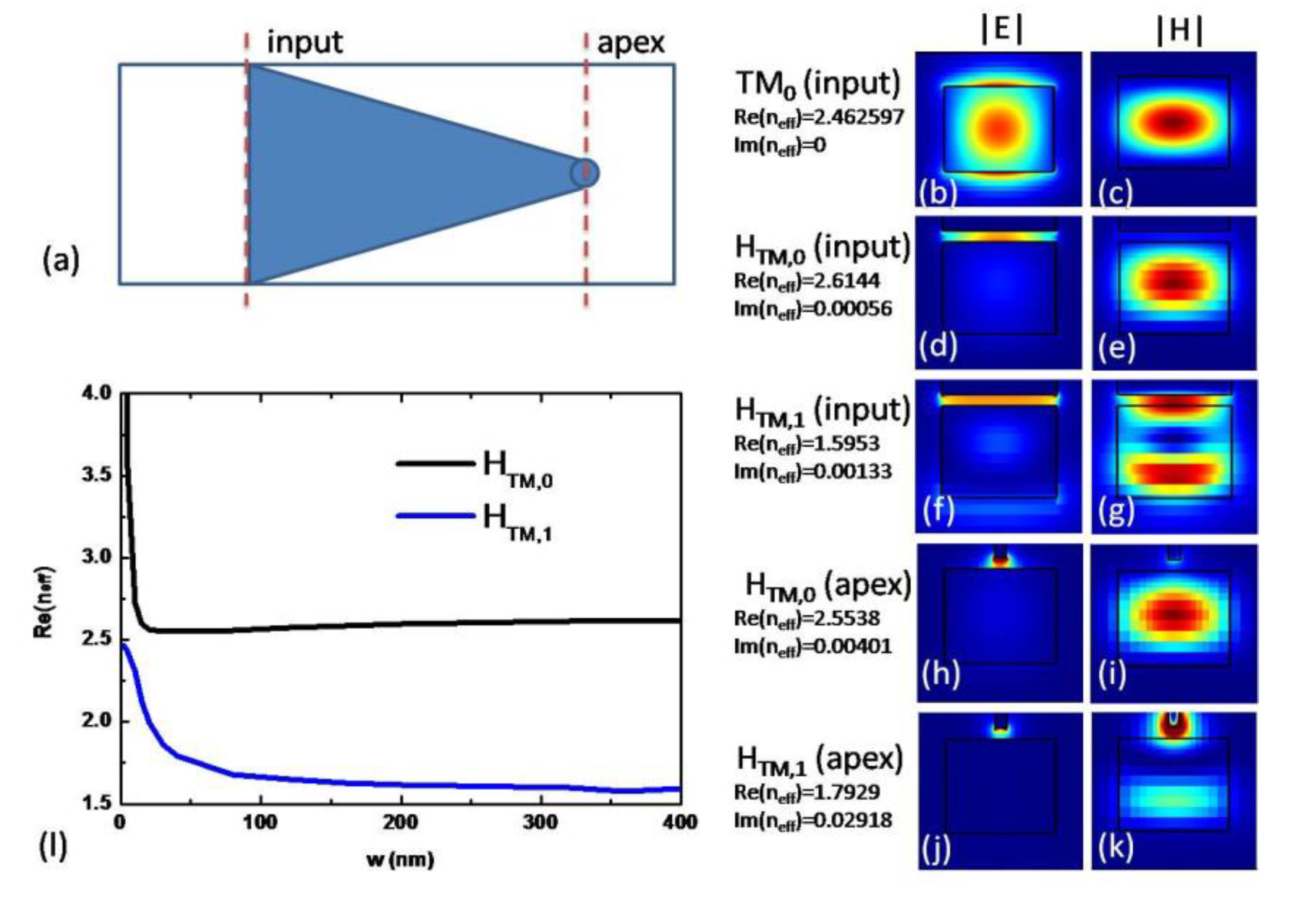
3.2. Mode Analysis of the Plasmonic Memristor

There are two types of modes existing in the plasmonic taper, TE-like modes and TM-like modes [28], but the TM-like modes are of more of interest because they can be focused at the tip of the triangle, as opposed to the TE modes. Hence, in the following, we naturally focus on the TM-like modes in the taper (Figure 2a). As specified for the incident fundamental TM photonic mode of the Si waveguide at a wavelength of 1550 nm (Figure 2b,c), the HTM, 0 and HTM, 1 super modes can be excited at the input of the plasmonic taper (i.e., at w = 400 nm, see Figure 2d–g). The width of the taper gradually decreases from w = 400 nm at the input to w = 0 nm at the apex (their mode profiles at the place near the apex with a narrow taper width of 40 nm are shown in Figure 2h–k), which can be confirmed from the dependence of the effective index of these modes on the taper width, as shown in Figure 2l. It can be clearly observed that for either of the HTM, 0 and HTM, 1 modes, the electrical field is tightly confined in the SiO2 layer. Meanwhile, their distribution is always under the metal zone, such that the HTM, 0 and HTM, 1 modes are highly overlapped with each other in the taper, and, accordingly, they propagate through the plasmonic nano-taper and could couple via directional coupling mechanism [28].
As specified for the HTM, 0 and HTM, 1 modes, the beat length (BL), given by the length over which the relative phase of the super modes differs by 2π, is inversely proportional to the real part of the difference between their effective indices, and can be obtained as follows [28]:
B L ( w ) = λ / Re ( Δ n e f f ( w ) )
where λ is the operation wavelength, and Δneff is the difference between the effective index of HTM, 0 and that of HTM, 1. Obviously, BL decreases as the light propagates along the triangle because the effective index of HTM, 0 increases steeply as the width of the triangle nanotaper decreases, as shown in Figure 2l. Finally, the effective index of HTM, 0 increases asymptotically to infinity, as the effective index of HTM, 1 is less than 2.5 (Figure 2l), and, thus, the BL approaches zero at the apex of the triangle taper, where the group velocity asymptotically approaches zero. Consequently, the electromagnetic energy is horizontally focused at the apex of the taper. Such a light localization process is common to most geometry-induced nano-focusing based on structures such as the plasmonic taper shown here [31], and serves as one of the main mechanisms to produce extreme light concentration (Figure 1c). Moreover, we check the light-leaking during the focusing by the adiabatic theory. Especially, using the Wentzel−Kramers−Brillouin (WKB) approximation, the aneikonal parameter (also called adiabatic parameter) can be defined as [31]:
δ = | ( d w / d x ) ( d ( k 0 n e f f ) 1 / d x ) |
where k0 and neff are the wavevector in vacuum and the effective index of the HTM, 0 mode, respectively. The eikonal parameter for the HTM, 0 mode (the main adiabatically changing mode when the width w is tapered down) is less than 0.5 (dw/dx) when w > 16 nm, indicating quite-low light-leaking generated in this geometry focusing process. Besides geometry focusing, another critical factor for the light concentration in our plasmonic memristor is the optimal energy transfer from the dielectric waveguide to the plasmonic taper [28]. In particular, for a taper with length L, the following applies:
0 L d z B L ( w ) = ( 0 L Δ n e f f ( w ) d z ) / λ = 1 / 2
where z is the position away from the input end, and w is the width of the metal taper at position z. Here w is determined by the width at the input end (W = 400 nm) and the taper length L with w(z) = W(Lz)/L, if the shape imperfection due to apex-rounding are ignored. Then, the light energy could be vertically coupled efficiently into the SiO2 buffer layer at the apex of the taper (Figure 1d). The combination of geometry-induced horizontal focusing and optimal energy transfer to the plasmonic taper would maximize the light concentration in the SiO2 buffer layer at the apex of the taper, which is overlapped with the memristive area where the filament could form or dissolve. This is the key to achieving a high extinction efficiency.

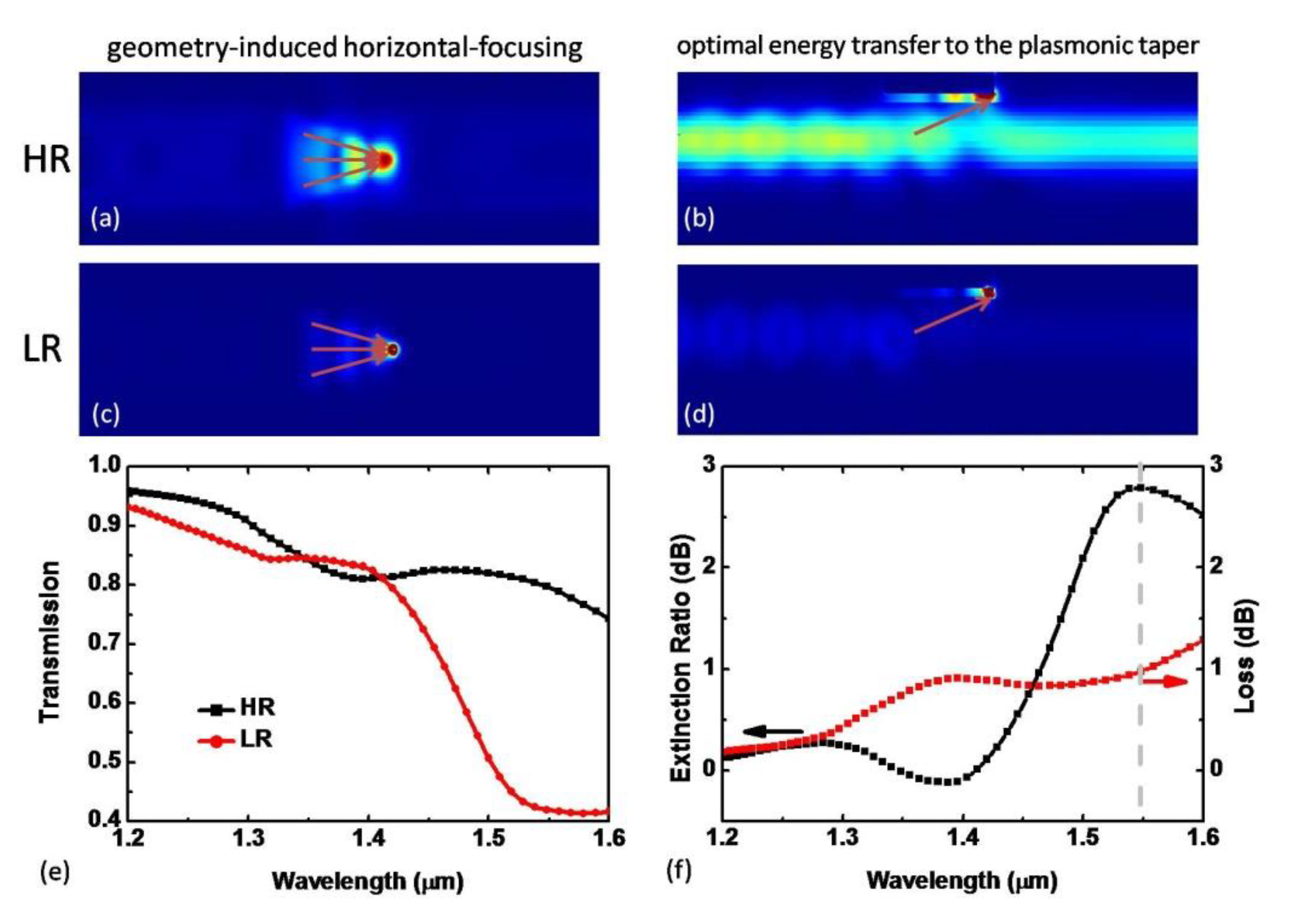
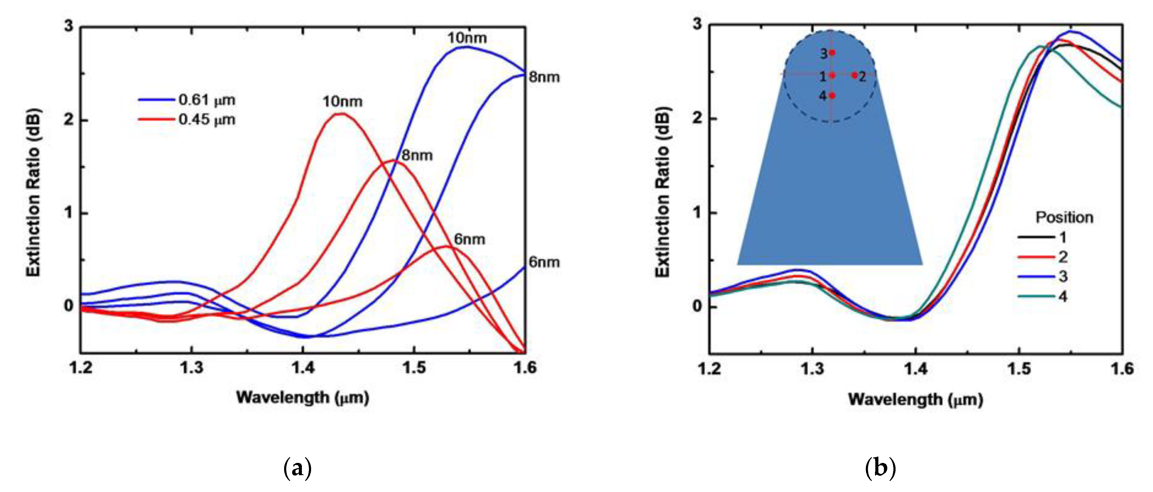
3.3. The Properties of the Plasmonic Memristor with Specified Size

The performance of the plasmonic memristor can be evaluated by checking its optical transmission at the HR stateand LRstate, as well as comparing their difference via a finite-difference time-domain (FDTD, Lumerical solution) simulation. A mode source (TM0, see Figure 2b) supported by the Si waveguide is feed in at the input side and propagates to the taper apex. When the plasmonic memristor is at the HR state, the incident light will go forwards continuously along the Si waveguide. Consequently, the monitor that detects the output light would receive a strong signal, i.e., the plasmonic memristor at the HR state is highly transparent for the TM0 incident source; while, for the device at the LR state, metal filaments would form in the SiO2 buffer layer, resulting in the light absorbing and scattering. Accordingly, low light transmission is produced. The transmission difference between the HR and LR state could be a qualitative reflection of the plasmon–filament interaction, and could be used to evaluate the performance of the plasmonic memristor. Although, in the real device, the size, shape and/or site of the filament could be highly random, without the loss of generality, here, we set our plasmonic memristor at the LR state, with a circular filament in the SiO2 buffer layer under the taper apex, located at the center of the circle, as marked in Figure 2a. The diameter of the filament is set as ~10 nm, according to Refs. [32,33,34] (the geometric influence of the filament will be discussed in detail in Section 3.5).
The specific size of the taper, as well as the Si waveguide, is as shown in Figure 1c,d; however, since L is governed by an integral equation (Equation (3)), and neff(w) in this equation is not given in an analytical form, but from the numerical calculated effective index of the HTM, 0 and HTM, 1 modes at different widths w, it is quite difficult to explicitly determine the taper length by Equation (3). However, considering that the BL of the triangular taper can be approached by BL (wavg) [28], where wavg is the average metallic width over the taper length, corresponding to about 1/2 of the maximum width W of the taper (i.e., wavg ≈ W/2 = 200 nm), we obtain the following:
Δ n e f f ( w a v g ) L λ / 2 o r L λ 2 Δ n e f f ( w a v g )
It is noteworthy that from the calculation based on Equation (4), we cannot obtain a precise value of the optimal L because neff(w) would become very large as w is small, and the initial phase difference between HTM, 0 and HTM, 1 at the input side is not taken into account. As a result, 0 L Δ n e f f ( w ) d z would be underestimated by neff(wavg)L, resulting in the overestimation of the rational taper length from Equation (4). However, such an approach, as well as the proportional relationship between the taper length and the wavelength revealed from it, still gives us the clues to obtain the rational initial design and/or the guideline for further structure optimization. The optimized length L is 610 nm to produce the maximum extinction ratio at the telecommunication wavelength of 1.55 μm (the details of the optimization will be discussed, together with the taper length dependence of the properties of the plasmonic memristor, in Section 3.4). In this structure, geometry-induced horizontal focusing can be clearly observed in Figure 3a, and the optimal energy transfer to the plasmonic taper is also achieved (Figure 3b). These two effects co-produce the strong plasmon–filament interaction as the device is switched to the LR state, as shown in Figure 3c,d. From the optical transmission features (Figure 3e), it is found that its LR and HR states correspond to two distinct spectra, TLR (λ) and THR (λ), especially around the C-band (~1.55 μm). Accordingly, it produces an extinction ratio (defined as −10l g (TLR/THR)) of 2.8 dB at the wavelength 1550 nm (Figure 3f), equivalent to the extinction efficiency of 4.6 dB/μm. Moreover, as this design has a compact size (overall length is 610 nm) much shorter than other structures [10,14,35], the intrinsic propagation loss of the plasmonic taper, positively correlated to its length, is reduced [36], resulting in a quite low loss of typically ~1 dB around 1550 nm (Figure 3f). Although the properties of the device discussed in this work are evaluated based on the simulations, and are perhaps not suitable to directly compare with the experimental reports summarized in Table 1 [10,14,19,20,35,37], the achieved results still imply that introducing the small triangle-shaped metal taper on top of the dielectric waveguide could be a promising design for a plasmonic memristor with superior performances. However, it is noteworthy that at the other important communication window (1.31 μm, O-band), the spectra change induced by the memristive switching is much weaker, and in an even shorter wavelength range, and the transmission spectra of the device at the HR state become very close to that at the LR state (see Figure 3e and Figure 4); hence, in the following, we mainly focus on the 1.55 μm range.

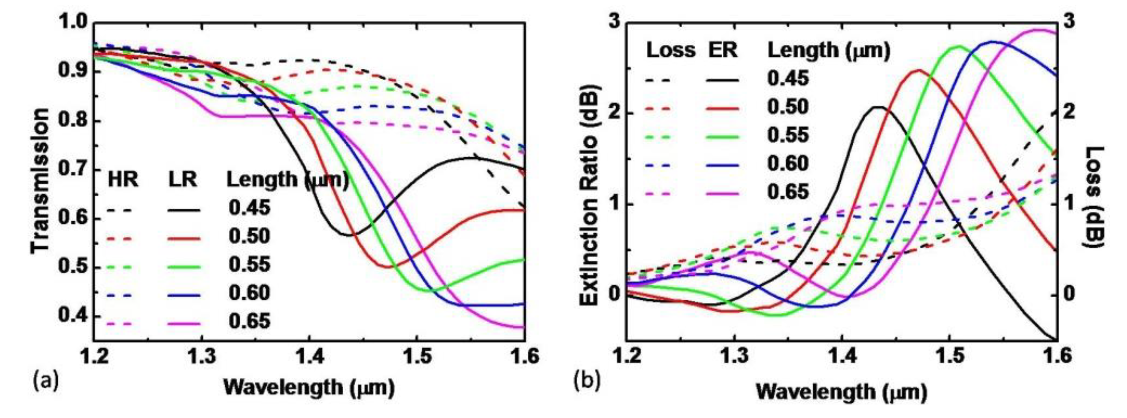
3.4. Taper Length Dependence of the Properties of the Plasmonic Memristor

Initially, we estimate the optimal taper length (=791 nm) by Equation (4), and simulate the optical response of this structure at both the LR and HR states. It founds a maximum extinction ratio at a relatively longer wavelength out of the telecommunication window. However, as the taper length is gradually reduced, a high ER at the C-band can be achieved, and, finally, we can obtain the best ER when the taper length is 610 nm, as proposed above. To further study the influences of the taper length on our plasmonic memristor around the C-band, in this section, we discuss the transmission spectra of the plasmonic memristor (in both the HR and LR states) with different metallic taper lengths, from 0.65 μm to 0.45 μm.
Figure 4a shows that the transmission T of the plasmonic memristor (at the HR state) is generally at a high level (from 0.95 to 0.6, depending on the taper length) at wavelengths from 1.2 μm to 1.6 μm. Accordingly, the insertion loss of the plasmonic memristor is typically 1~2 dB at the C-band (Figure 4b). Such a low loss in our design, compared with other reported structures, is due to the compact size, which reduces the intrinsic propagation loss of the plasmonic taper as discussed above; while, at the LR state, the transmission of the plasmonic memristor clearly decreases, indicating the remarkable extinction due to the formation of the filament (Figure 4a). When the taper length changes from 0.65 μm to 0.45 μm, the maximum extinction ratio shifts from 1.43 μm to 1.58 μm. This is because of the positive correlation between the operation wavelength and the optimal taper length, which can be quantitatively observed from Equation (4). However, along with the shorting of the taper length, the extinction ratio decreases, as shown in Figure 4b. This is ascribed to the subsiding of the geometry-induced horizontal focusing for the short taper. Actually, according to the adiabatic theory based on the WKB approximation [31], for the long taper with a small dw/dx, its adiabatic parameter δ, defined by Equation (2), is accordingly small, and, subsequently, the geometric focusing of the light would be close to the ideal adiabatic focusing, while, for the shorter taper (large dw/dx), the δ increases, and thus the light concentration becomes non-adiabatic, i.e., not all the light input into the taper could be concentrated to its apex—some light energy leaks out of the taper and does not contribute to the plasmon-filament interaction [31].

3.5. Filament Dependence of the Properties of the Plasmonic Memristor

Other than the circular column filament with a radius of 10 nm, considered in the aforementioned simulations, the filament in the cycled operations to the memristor has a different size and shape, and forms randomly at different sites of the insulator layer between the two electrodes [24,26]. The influences of these factors should be investigated. The recent work, based on kinetic Monte Carlo simulation, shows that the extinction behavior of the filament should be insensitive to its shape, but mainly governed by its size [32], so without the loss of generality, we fix the shape of the filament as the circular column, as conducted above, and check the extinction produced by the filament with a different radius, to evaluate the filament size-dependent properties of the plasmonic memristor. On the other hand, to understand the effects of the randomness of the filament site, which is a regular phenomenon existing in the memristor [24], we also study the variation in extinction due to the change in the position of the filament.
Figure 5a shows that for the taper with a length of 0.61 μm, as the filament radius decreases from 10 nm to 6 nm, the extinction peak red-shifts remarkably and moves out of the C-band. As a result, the extinction ratio at 1.55 μm decreases from 2.8 dB to 0.02 dB (accordingly the extinction efficiency changes from 4.6 dB/μm to 0.033 dB/μm). Similarly, for the taper with a length of 0.45μm, as the filament radius decreases from 10 nm to 6 nm, the extinction peak red-shifts from 1.43μm to 1.53 μm, and the maximum extinction ratio changes from 2.08 dB to 0.65 dB (corresponding to the change in the extinction efficiency from 4.62 dB/μm to 1.44 dB/μm). Therefore, it can be concluded that the extinction induced by the formation of the filament is positively correlated to its size. Meanwhile, it is noteworthy that the smaller the filament, the longer the peak wavelength of the extinction. The filament size dependence of the extinction behavior is very similar to the spectra features of the electrochemically programmable plasmonic antennas observed very recently [32]. Such a similarity indicates that the absorption and scattering of the filament to the plasmon, as proposed in previous research about the extinction mechanism of the plasmonic memristor [10,14], may be highly affected by the transition of the localized resonant plasmonic mode (e.g., in the electrochemically programmable plasmonic antennas, the formation of the filament results in the transition from a bonding dipole plasmon to a charge transfer plasmon) [32]. Therefore, checking the possible influences of the resonance transition of the hybrid plasmon in the MIS structure might be beneficial for us to further improve the device’s performance.
Figure 5b shows the extinction behavior that is dependent on the position of the filament. It was found that, for the filament with a fixed size, the closer its position to the apex, the higher the extinction ratio obtained. This is a quite natural result, since in our design, the electromagnetic energy of the plasmon is truly concentrated to the apex, due to the combination of geometry-induced horizontal focusing and optimal energy transfer from the Si waveguide to the plasmonic taper, as discussed above. However, other than the size of the filament, the extinction behavior of the plasmonic memristor is much less sensitive to the variation in the filament position. Therefore, practically, to achieve repeatable memristive operation of the plasmon, it is more critical to stabilize the filament size in comparison with reducing the randomness of the filament site. Fortunately, thanks to the increasingly deep understanding of the mechanisms of the memristor [24,38,39], as well as the uninterrupted development of the strategy to control the filament growth in the memristors over the last few years [40,41], it is believable that the plasmonic memristor could become more repeatable and stable.

4. Conclusions

In this paper, we propose a design of a plasmonic memristor working at a telecom wavelength of 1.55 μm, with a compact size (0.61 μm), low insertion loss (1 dB), and high extinction efficiency (4.6 dB/μm). It consists of a triangle Ag taper integrated on the Si waveguide with a SiO2 buffer layer. In this structure, the Ag taper serves as both the top electrode of the memristor and light concentrator, due to the combination of geometry-induced horizontal focusing and optimal energy transfer to the taper. The rational doping to the Si waveguide in the area below the apex of the taper defines the bottom electrode and, accordingly, confines the zone in which the memristive behaviors (formation and rupture of the filament) occur in the area near the apex. As a result, the interactions between the plasmon and the filament in the memristor could be maximized. We point out that the key to improving the repeatable and stable plasmonic memristor is the effective control of the filament size. Our work might be valuable to improve the plasmonic memristor, as well as promote its application in on-chip optical memory, opto-electrical hybrid synapse, etc.

Author Contributions

Conceptualization, Y.T. and S.Z; simulations, Y.T.; writing—original draft preparation, Y.T.; writing—review and editing, Y.T., S.Z. and W.T. All authors have read and agreed to the published version of the manuscript.

Funding

This research was supported by NSFC (11947088, U1832143), Hunan Provincial Natural Science Fund (2019JJ50025) and the Scientific Research Fund of Hunan Provincial Education Department (No. 19B100).

Data Availability Statement

All data included in this study are available upon request by contact with the corresponding author.

Conflicts of Interest

The authors declare no conflict of interest.

References

  1. Soref, R. The Past, Present, and Future of Silicon Photonics. IEEE J. Sel. Top. Quantum Electron. 2006, 12, 1678–1687. [Google Scholar] [CrossRef]
  2. Melikyan, A.; Koehnle, K.; Lauermann, M.; Palmer, R.; Koeber, S.; Muehlbrandt, S.; Schindler, P.; Elder, D.; Wolf, S.; Heni, W.; et al. Plasmonic-organic hybrid (POH) modulators for OOK and BPSK signaling at 40 Gbit/s. Opt. Express. 2015, 23, 9938–9946. [Google Scholar] [CrossRef] [PubMed] [Green Version]
  3. Melikyan, A.; Alloatti, L.; Muslija, A.; Hillerkuss, D.; Schindler, P.C.; Li, J.; Palmer, R.; Korn, D.; Muehlbrandt, S.; Van Thourhout, D.; et al. High-speed plasmonic phase modulators. Nat. Photon. 2014, 8, 229–233. [Google Scholar] [CrossRef]
  4. Barnes, W.L.; Dereux, A.; Ebbesen, T.W. Surface plasmon subwavelength optics. Nature 2003, 424, 824–830. [Google Scholar] [CrossRef]
  5. Tian, Y.; Jiang, L.; Deng, Y.; Deng, S.; Zhang, G.; Zhang, X. Bi-nanorod/Si-nanodot hybrid structure: Surface dewetting induced growth and its tunable surface plasmon resonance. Opt. Mater. Express 2015, 5, 2655–2666. [Google Scholar] [CrossRef]
  6. Yang, J.; Perrin, M.; Lalanne, P. Analytical Formalism for the Interaction of Two-Level Quantum Systems with Metal Nanoresonators. Phys. Rev. X 2015, 5, 021008. [Google Scholar] [CrossRef]
  7. Pile, D.F.; Ogawa, T.; Gramotnev, D.K.; Matsuzaki, Y.; Vernon, K.C.; Yamaguchi, K.; Okamoto, T.; Haraguchi, M.; Fukui, M. Two-dimensionally localized modes of a nanoscale gap plasmon waveguide. Appl. Phys. Lett. 2005, 87, 261114. [Google Scholar] [CrossRef] [Green Version]
  8. Nikolajsen, T.; Leosson, K.; Bozhevolnyi, S.I. Surface plasmon polariton based modulators and switches operating at telecom wavelengths. Appl. Phys. Lett. 2004, 85, 5833–5835. [Google Scholar] [CrossRef]
  9. Heeres, R.W.; Dorenbos, S.N.; Koene, B.; Solomon, G.S.; Kouwenhoven, L.P.; Zwiller, V. On-chip single plasmon detection. Nano Lett. 2009, 10, 661–664. [Google Scholar] [CrossRef] [PubMed] [Green Version]
  10. Emboras, A.; Goykhman, I.; Desiatov, B.; Mazurski, N.; Stern, L.; Shappir, J.; Levy, U. Nanoscale Plasmonic Memristor with Optical Readout Functionality. Nano Lett. 2013, 13, 6151–6155. [Google Scholar] [CrossRef]
  11. Strukov, D.B.; Snider, G.S.; Stewart, D.R.; Williams, S. The missing memristor found. Nature 2008, 453, 80–83. [Google Scholar] [CrossRef] [PubMed]
  12. Mehonic, A.; Cueff, S.; Wojdak, M.; Hudziak, S.; Jambois, O.; Labbé, C.; Garrido, B.; Rizk, R.; Kenyon, A. Resistive switching in silicon suboxide films. J. Appl. Phys. 2012, 111, 074507. [Google Scholar] [CrossRef]
  13. Tian, Y.; Guo, C.; Guo, S.; Yu, T.; Liu, Q. Bivariate-continuous-tunable interface memristor based on Bi2S3 nested nano-networks. Nano Res. 2014, 7, 953–962. [Google Scholar] [CrossRef]
  14. Hoessbacher, C.; Fedoryshyn, Y.; Emboras, A.; Melikyan, A.; Kohl, M.; Hillerkuss, D.; Hafner, C.; Leuthold, J. The plasmonic memristor: A latching optical switch. Optica 2014, 1, 198. [Google Scholar] [CrossRef]
  15. Di Martino, G.; Tappertzhofen, S.; Hofmann, S.; Baumberg, J. Nanoscale Plasmon-Enhanced Spectroscopy in Memristive Switches. Small 2016, 12, 1334–1341. [Google Scholar] [CrossRef] [Green Version]
  16. Koch, U.; Hoessbacher, C.; Emboras, A.; Leuthold, J. Optical memristive switches. J. Electroceramics 2017, 39, 239–250. [Google Scholar] [CrossRef] [Green Version]
  17. Borghetti, J.; Snider, G.S.; Kuekes, P.J.; Yang, J.J.; Stewart, D.R.; Williams, R.S. Memristive’switches enable ‘stateful’ logic operations via material implication. Nature 2010, 464, 873–876. [Google Scholar] [CrossRef]
  18. Kvatinsky, S.; Kolodny, A.; Weiser, U.C.; Friedman, E.G. Memristor-based IMPLY logic design procedure. In Proceedings of the 2011 IEEE 29th International Conference on Computer Design (ICCD), Amherst, MA, USA, 9–12 October 2011; pp. 142–147. [Google Scholar]
  19. Parra, J.; Olivares, I.; Brimont, A.; Sanchis, P. Non-volatile epsilon-near-zero readout memory. Opt. Lett. 2019, 44, 3932–3935. [Google Scholar] [CrossRef]
  20. Singh, L.; Jain, S.; Kumar, M. Electrically writable silicon nanophotonic resistive memory with inherent stochasticity. Opt. Lett. 2019, 44, 4020–4023. [Google Scholar] [CrossRef]
  21. Ríos, C.; Youngblood, N.; Cheng, Z.; Le Gallo, M.; Pernice, W.H.P.; Wright, C.D.; Sebastian, A.; Bhaskaran, H. In-memory computing on a photonic platform. Sci. Adv. 2019, 5, eaau5759. [Google Scholar] [CrossRef] [Green Version]
  22. Xue, W.; Ci, W.; Xu, X.-H.; Liu, G. Optoelectronic memristor for neuromorphic computing. Chin. Phys. B 2020, 29, 048401. [Google Scholar] [CrossRef]
  23. Portner, K.; Schmuck, M.; Lehmann, P.; Weilenmann, C.; Haffner, C.; Ma, P.; Leuthold, J.; Luisier, M.; Emboras, A. Analog Nanoscale Electro-Optical Synapses for Neuromorphic Computing Applications. ACS Nano 2021, 15, 14776–14785. [Google Scholar] [CrossRef] [PubMed]
  24. Waser, R.; Dittmann, R.; Staikov, G.; Szot, K. Redox-based resistive switching memories–nanoionics mechanisms, prospects, and challenges. Adv. Mater. 2009, 21, 2632–2663. [Google Scholar] [CrossRef]
  25. Tian, Y.; Pan, L.; Guo, C.F.; Liu, Q. Atomic origin of the traps in memristive interface. Nano Res. 2016, 10, 1924–1931. [Google Scholar] [CrossRef]
  26. Sawa, A. Resistive switching in transition metal oxides. Mater. Today 2008, 11, 28–36. [Google Scholar] [CrossRef]
  27. Flammer, P.D.; Banks, J.M.; Furtak, T.E.; Durfee, C.G.; Hollingsworth, R.E.; Collins, R.T. Hybrid plas-mon/dielectric waveguide for integrated silicon-on-insulator optical elements. Opt. Express 2010, 18, 21013–21023. [Google Scholar] [CrossRef] [PubMed]
  28. Luo, Y.; Chamanzar, M.; Adibi, A. Compact on-chip plasmonic light concentration based on a hybrid pho-tonic-plasmonic structure. Opt. Expres. 2013, 21, 1898–1910. [Google Scholar] [CrossRef]
  29. Dong, P.; Liao, S.; Liang, H.; Shafiiha, R.; Feng, D.; Li, G.; Zheng, X.; Krishnamoorthy, A.V.; Asghari, M. Submilliwatt, ultrafast and broadband electro-optic silicon switches. Opt. Express 2010, 18, 25225–25231. [Google Scholar] [CrossRef] [PubMed]
  30. Chen, Y.; Shu, Z.; Zhang, S.; Zeng, P.; Liang, H.; Zheng, M.; Duan, H. Sub-10 nm fabrication: Methods and applications. Int. J. Extreme Manuf. 2021, 3, 032002. [Google Scholar] [CrossRef]
  31. Stockman, M.I. Nanofocusing of Optical Energy in Tapered Plasmonic Waveguides. Phys. Rev. Lett. 2004, 93, 137404. [Google Scholar] [CrossRef] [Green Version]
  32. Dong, S.; Zhang, K.; Yu, Z.; Fan, J.A. Electrochemically Programmable Plasmonic Antennas. ACS Nano 2016, 10, 6716–6724. [Google Scholar] [CrossRef] [PubMed]
  33. Ahn, Y.; Son, J.Y. The effect of size on the resistive switching characteristics of NiO nanodots. J. Phys. Chem. Solids 2016, 99, 134–137. [Google Scholar] [CrossRef]
  34. Ma, Y.; Yeoh, P.P.; Shen, L.; Goodwill, J.M.; Bain, J.A.; Skowronski, M. Evolution of the conductive filament with cycling in TaOx-based resistive switching devices. J. Appl. Phys. 2020, 128, 194501. [Google Scholar] [CrossRef]
  35. Emboras, A.; Niegemann, J.; Ma, P.; Haffner, C.; Pedersen, A.; Luisier, M.; Schimmel, T.; Leuthold, J. Atomic Scale Plasmonic Switch. Nano Lett. 2016, 16, 709–714. [Google Scholar] [CrossRef]
  36. Matsuzaki, Y.; Okamoto, T.; Haraguchi, M.; Fukui, M.; Nakagaki, M. Characteristics of gap plasmon wave-guide with stub structures. Opt. Express. 2008, 16, 16314–16325. [Google Scholar] [CrossRef]
  37. Singh, L.; Srivastav, S.; Kaushik, V.; Rajput, S.; Mishra, R.D.; Kumar, M. Light Assisted Electro-Metallization in Resistive Switch with Optical Accessibility. J. Light. Technol. 2021. [Google Scholar] [CrossRef]
  38. Tian, Y.; Zhang, J.; Guo, C.F.; Zhang, B.; Liu, Q. Photoconductive probing of the trap distribution in switchable interfaces. Nanoscale 2016, 8, 915–920. [Google Scholar] [CrossRef]
  39. Pan, F.; Chen, C.; Wang, Z.-S.; Yang, Y.-C.; Yang, J.; Zeng, F. Nonvolatile resistive switching memo-ries-characteristics, mechanisms and challenges. Prog. Nat. Sci. Mater. Int. 2010, 20, 1–15. [Google Scholar] [CrossRef] [Green Version]
  40. Wu, W.; Shan, B.; Feng, K.; Nan, H. Resistive switching behavior of Sb2S3 thin film prepared by chemical bath deposition. Mater. Sci. Semicond. Process. 2016, 44, 18–22. [Google Scholar] [CrossRef]
  41. Nardi, F.; Ielmini, D.; Cagli, C.; Spiga, S.; Fanciulli, M.; Goux, L.; Wouters, D. Control of filament size and reduction of reset current below 10μA in NiO resistance switching memories. Solid State Electron. 2011, 58, 42–47. [Google Scholar] [CrossRef]
Figure 1. (a) Memristive behaviors of Ag/SiO2/Si trilayer system; (b) conceptual illustration of the distinct interaction between plasmon and memristor at HR (upper) and LR (bottom) state; (c) three-dimensional visualization of the designed plasmonic memristor based on triangle-shaped metal taper on top of a dielectric wave guide (BOX: buried oxide); (d) top view; and (e) side view of the plasmonic memristor.
Photonics 08 00437 g001
Figure 2. (a) The concerned sites (input and apex as marked by red dashed lines) in the mode analysis to the plasmonic memristor; (b) electrical field and (c) magnetic field profile of the TM mode inputted from Si waveguide; (d) electrical field and (e) magnetic field profile of the HTM, 0 mode exited at the input of the taper (w = 400 nm); (f) electrical field and (g) magnetic field profile of the HTM, 1 mode exited at the input of the taper (w = 400 nm); (h) electrical field and (i) magnetic field profile of the HTM, 0 mode propagated to the apex of the taper (w = 40 nm); (j) electrical field and (k) magnetic field profile of the HTM, 1 mode propagated to the apex of the taper (w = 40 nm); (l) mode effective indices of HTM, 0 and HTM, 1 modes as the function of the width at different sites of silver taper.
Photonics 08 00437 g002
Figure 3. (a) Geometry-induced horizontal focusing and (b) optimal energy transfer to the taper of the plasmonic memristor at HR state; enhanced plasmon–filament interaction in the plasmonic memristor at LR state due to (c) geometry-induced horizontal focusing and (d) optimal energy transfer; (e) optical transmission of the plasmonic memristor at HR and LR state; (f) extinction ration (ER) and insertion loss of the plasmonic memristor.
Photonics 08 00437 g003
Figure 4. (a) Taper length dependence of the optical transmission of the plasmonic memristor at HR and LR states; (b) taper length dependence of the extinction ration (ER) and insertion loss of the plasmonic memristor.
Photonics 08 00437 g004
Figure 5. (a) Filament size dependence of the extinction ration (ER) of the plasmonic memristor; (b) filament position dependence of the optical transmission of the plasmonic memristor at HR and LR state.
Photonics 08 00437 g005
Table 1. Summary of the performances of some reported plasmonic memristors.
RefsDevice Length (μm) Loss (dB) extinction Ratio (dB) Extinction Efficiency (dB/μm)
[10]34.20.090.03
[14]5 (10) 18 (23) 6 (12) 1.2
[25]2.2259.24.2
[32] *,#50.2102
[33]5000/100.002
[34]1000/160.016
This work *0.6112.84.6
# Employ the epsilon-near-zero media between metal-like (plasmonic dispersion) and dielectric-like response; * numerical simulation results.
Publisher’s Note: MDPI stays neutral with regard to jurisdictional claims in published maps and institutional affiliations.

