Development and Analysis of a Modular LED Array Light Source


Abstract
1. Introduction
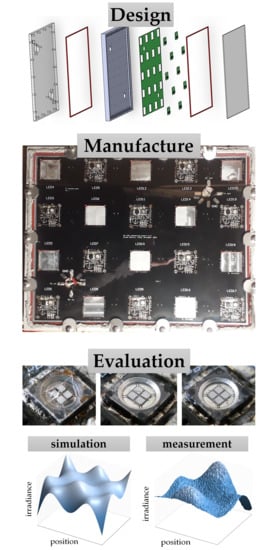
2. Array Design
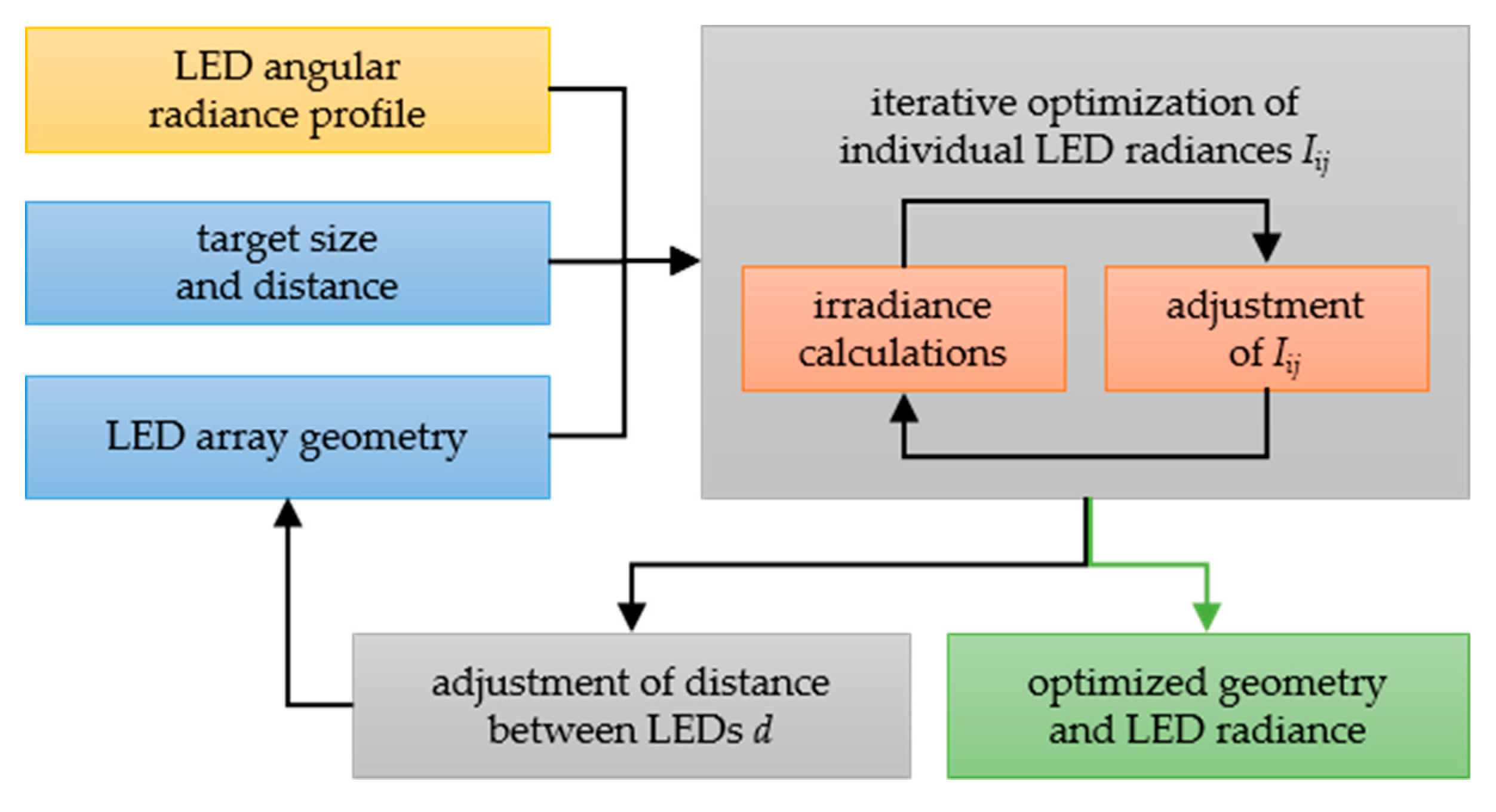
2.1. Irradiance Homogeneity Optimization
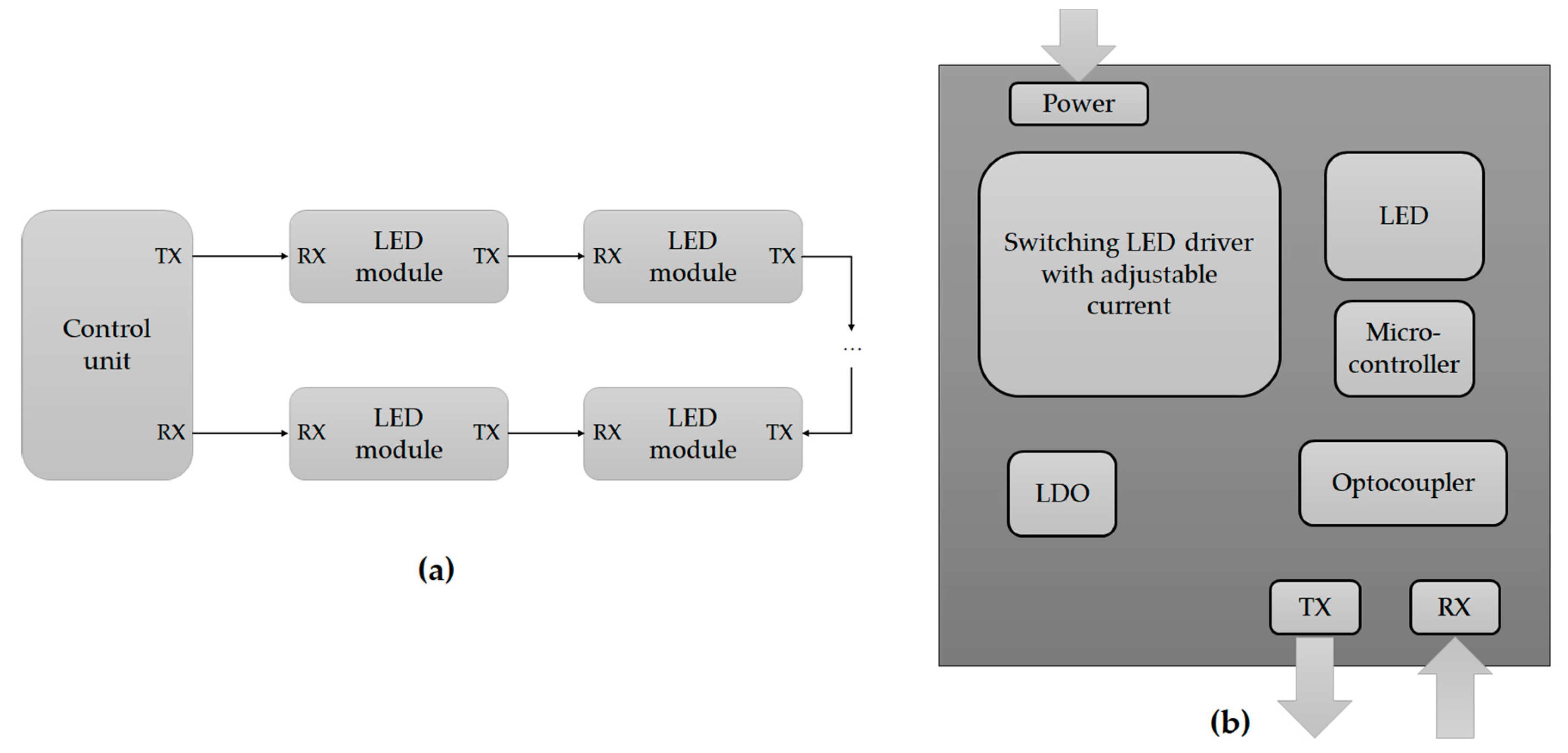
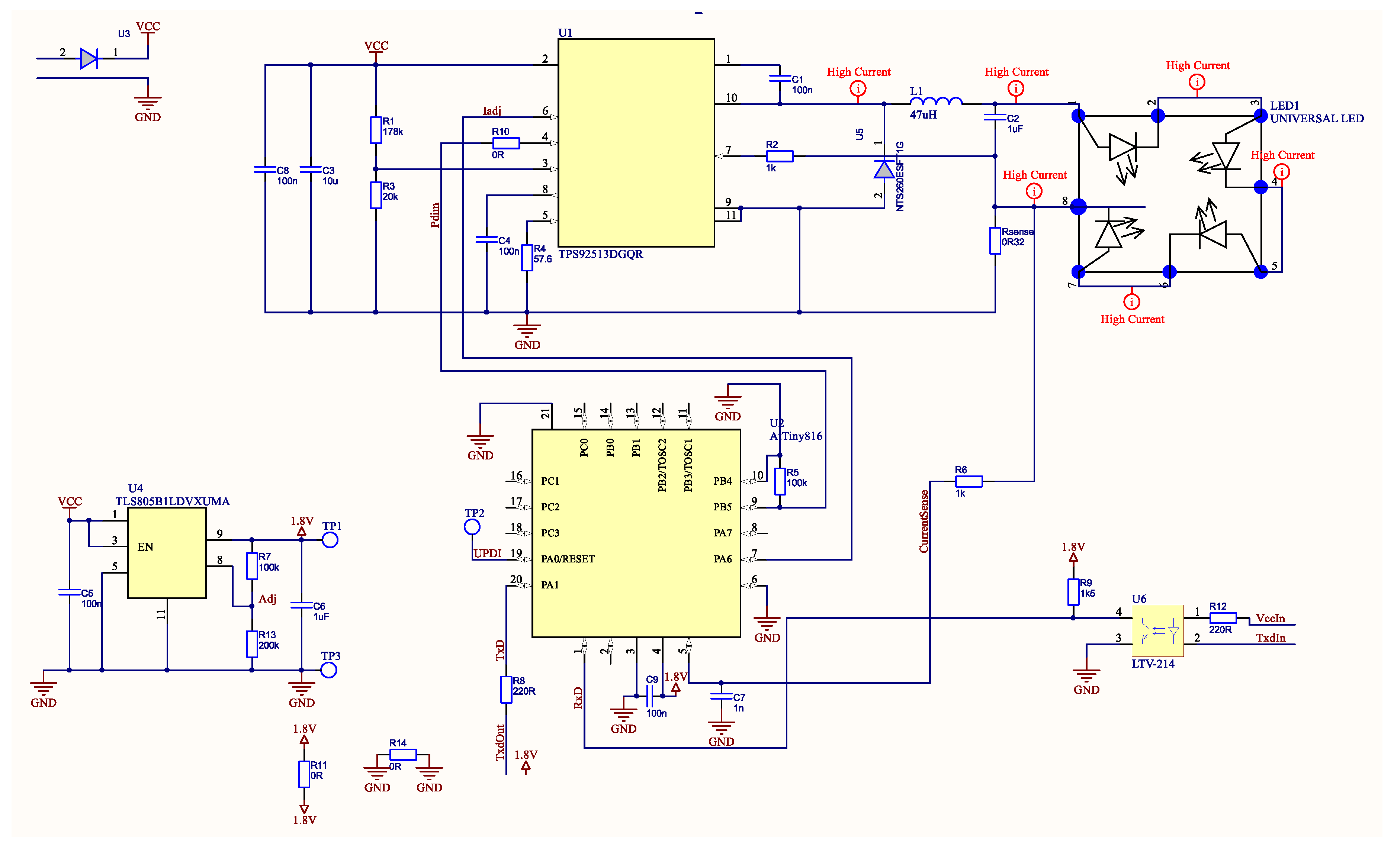
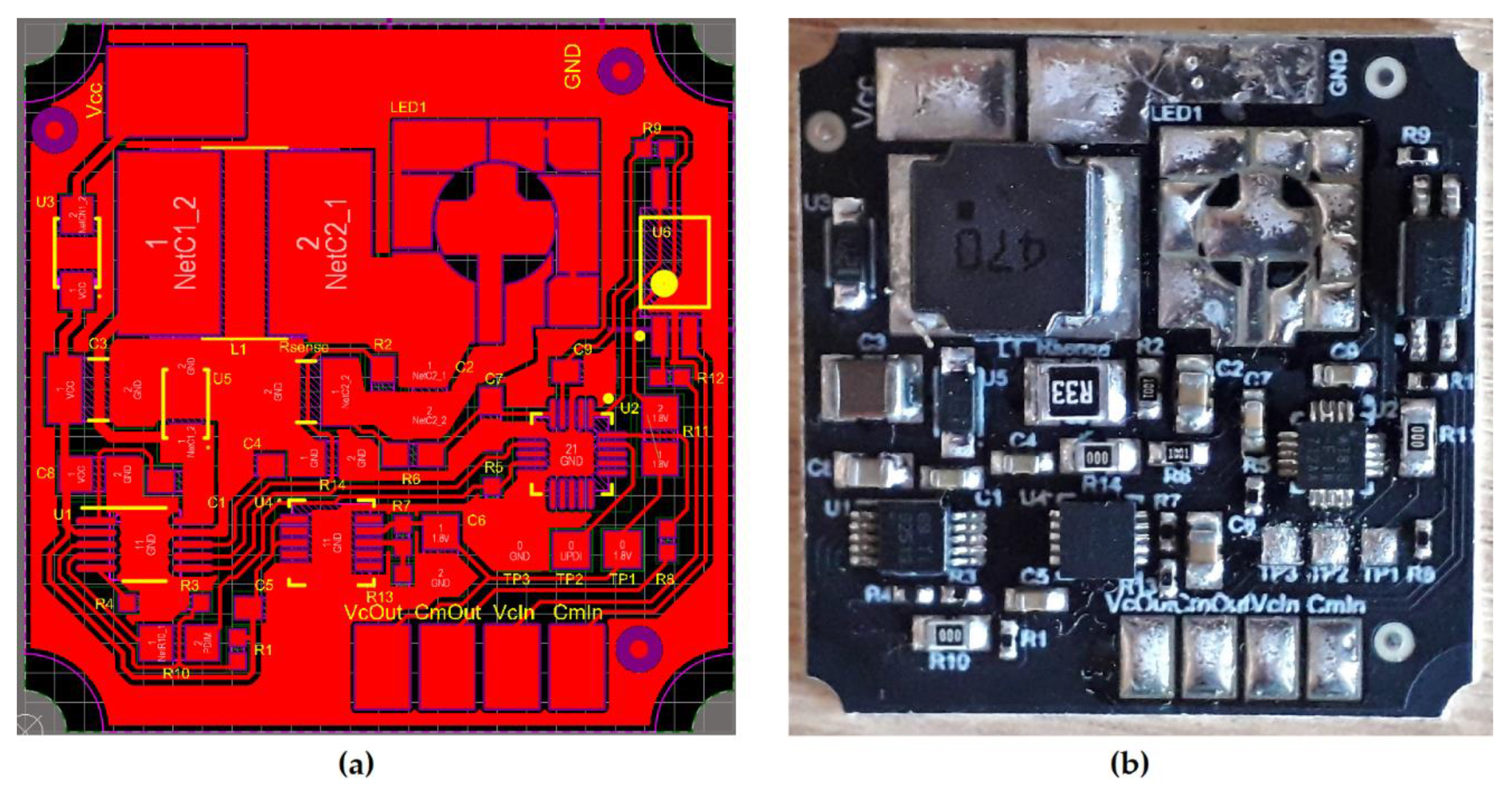
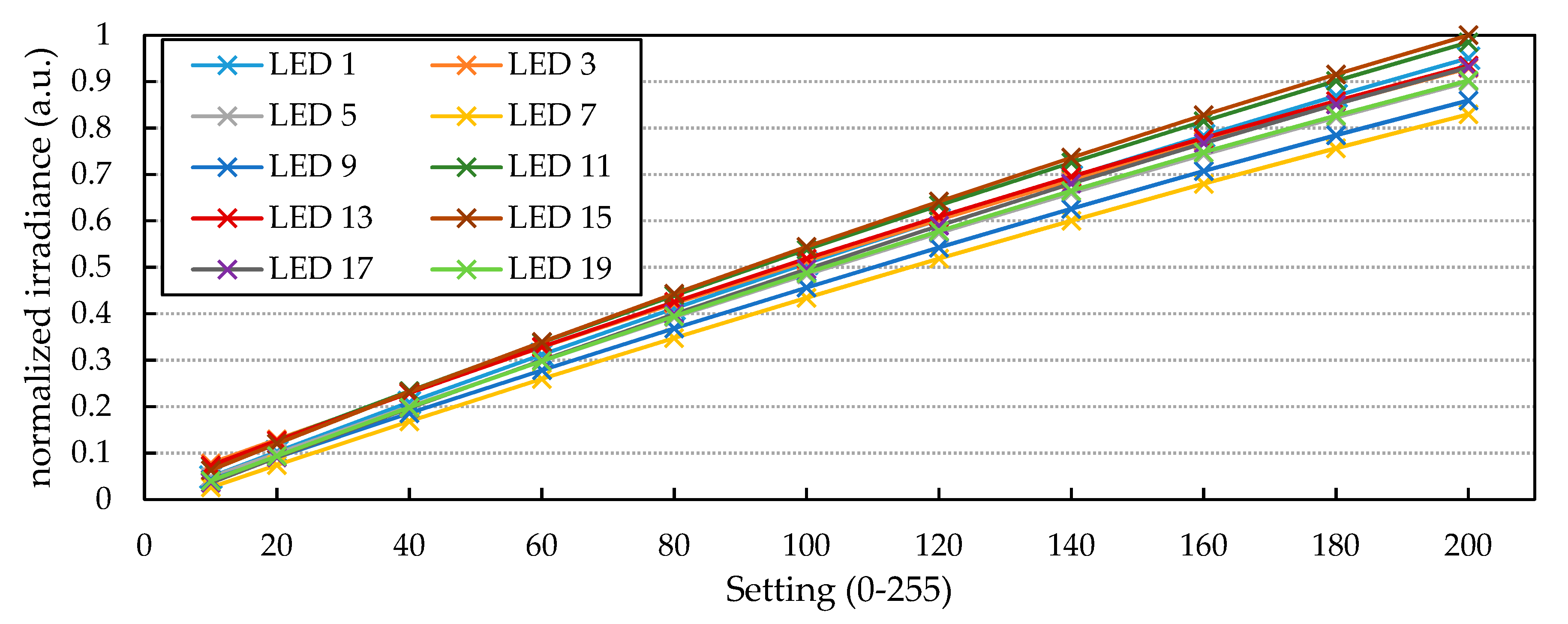
2.2. Electronic LED Drivers
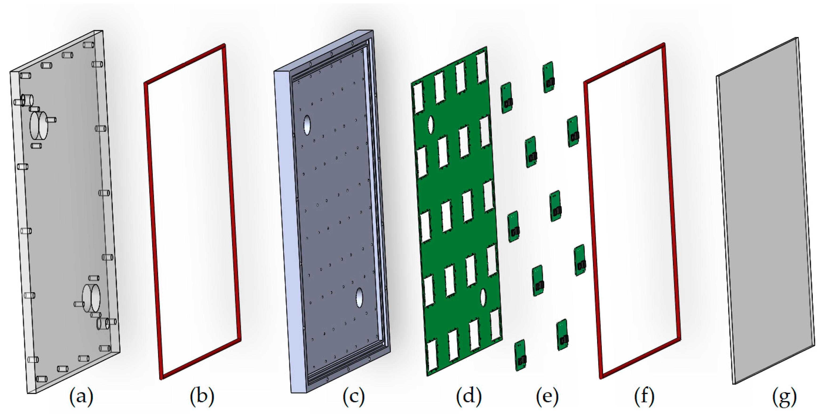
2.3. Mounting and Cooling of the Array
3. Array Prototype Characterization
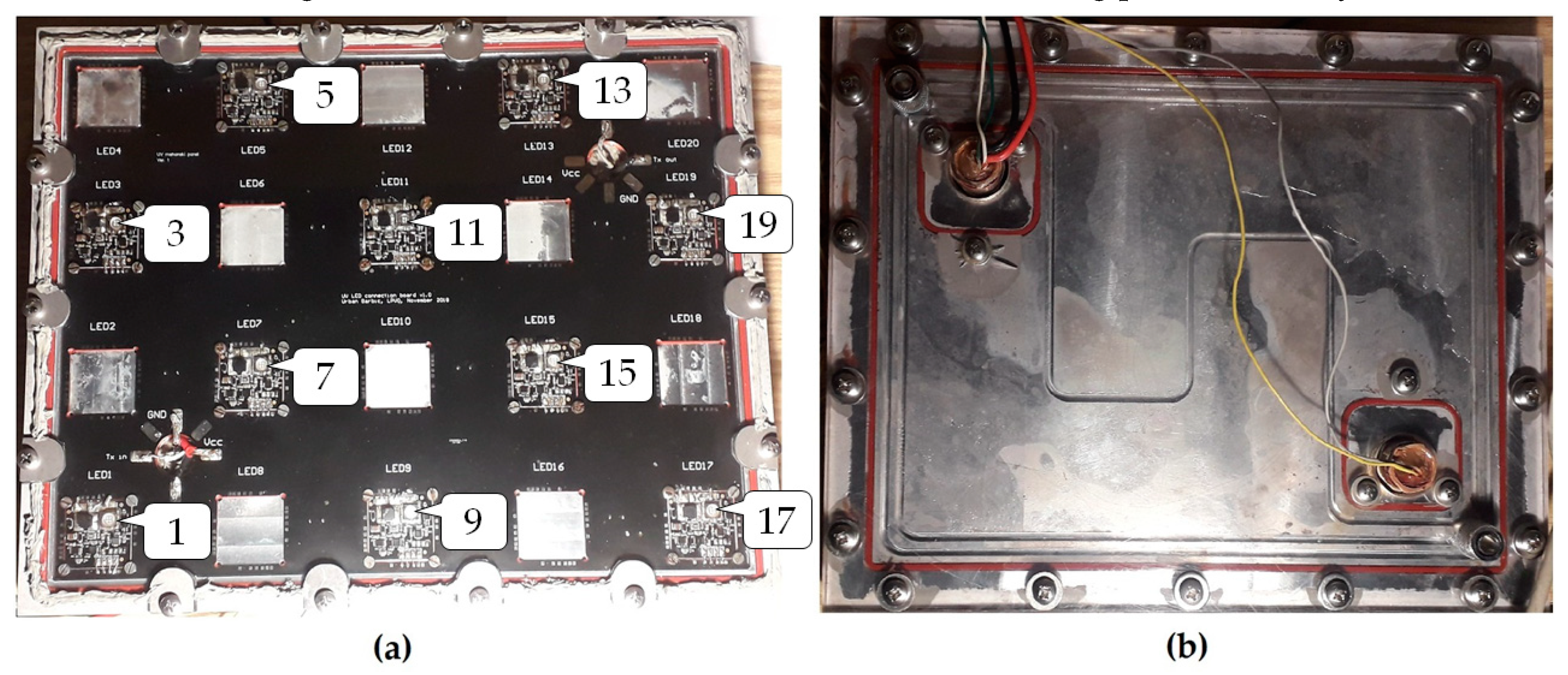
3.1. Array Manufacturing
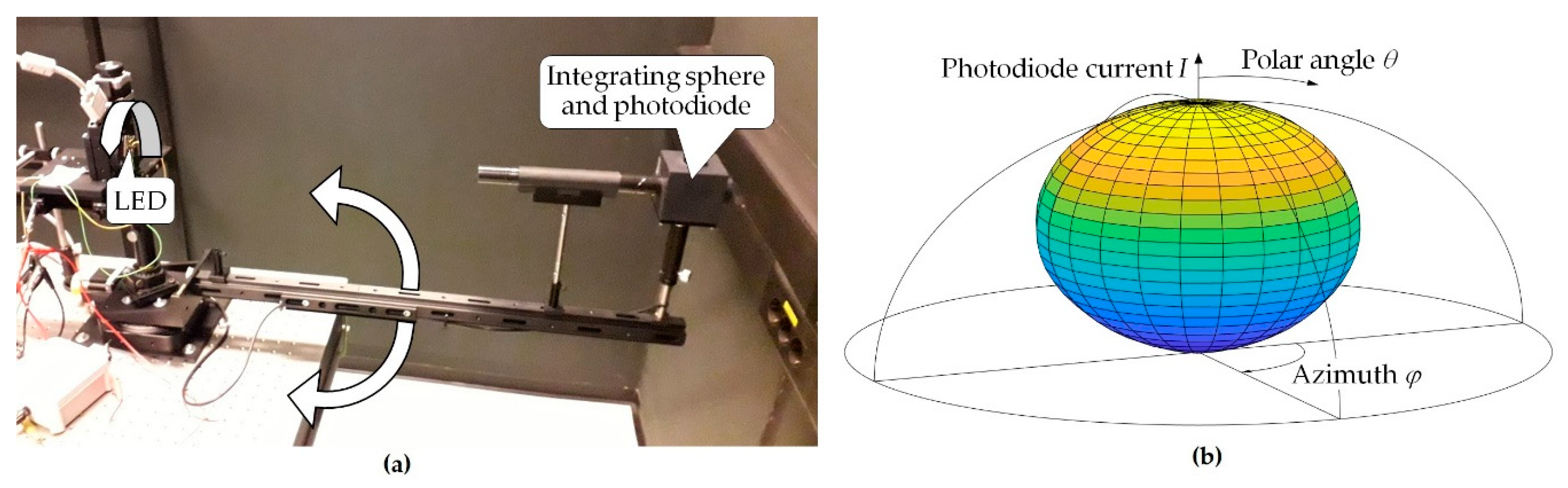
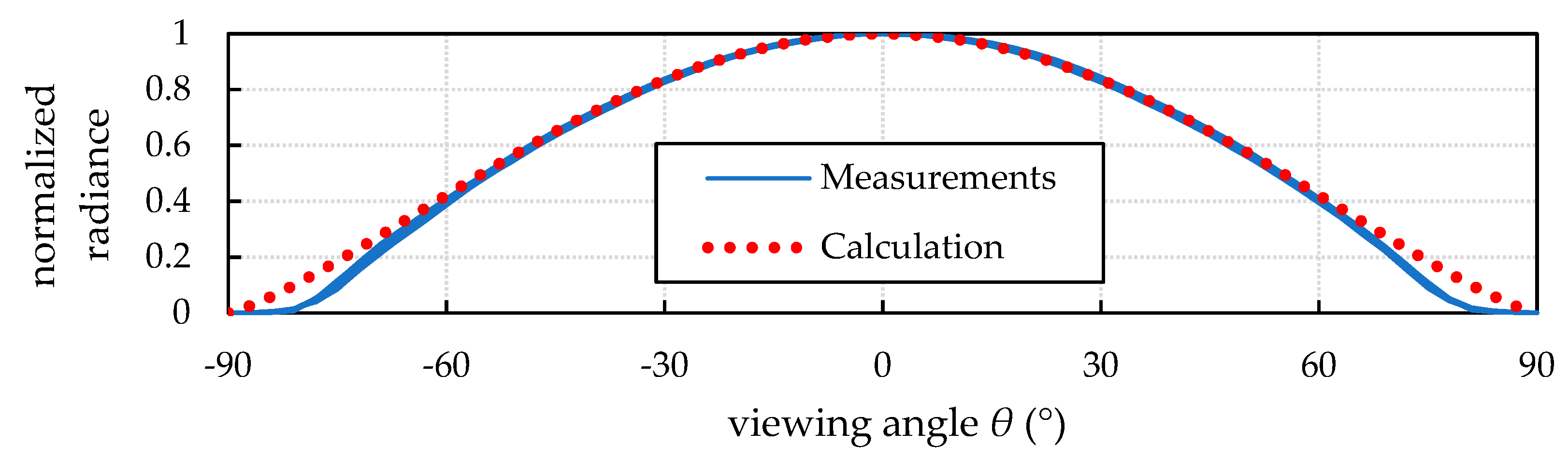
3.2. Angular LED Radiance
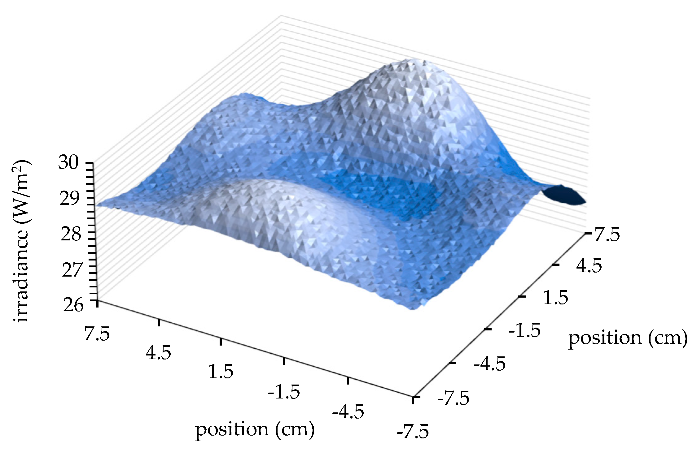
3.3. Spatial Irradiance Profile
3.4. Test in Climatic Chamber
4. Results
4.1. Driver Operation
4.2. Irradiance Homogeneity
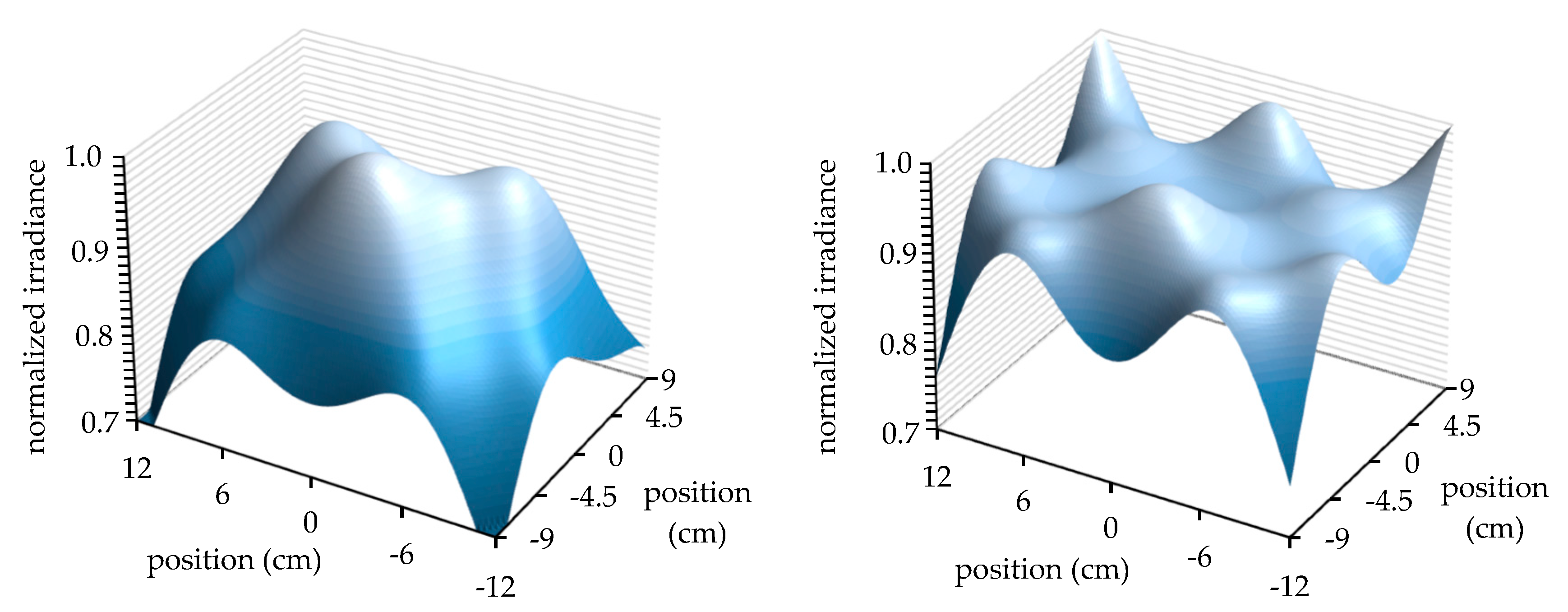
4.2.1. Optimization Method
4.2.2. Measurements
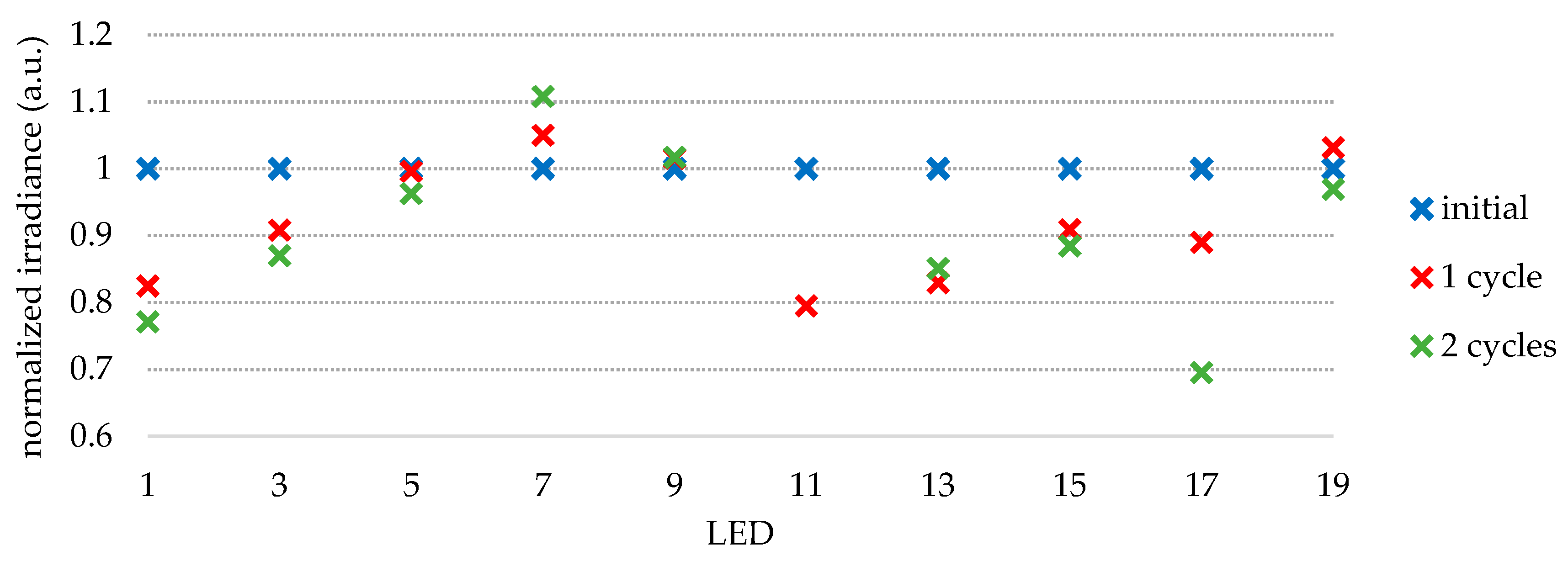
4.3. Characterization after Degradation
4.3.1. Total LED Radiance
4.3.2. LED Radiance Spectrum
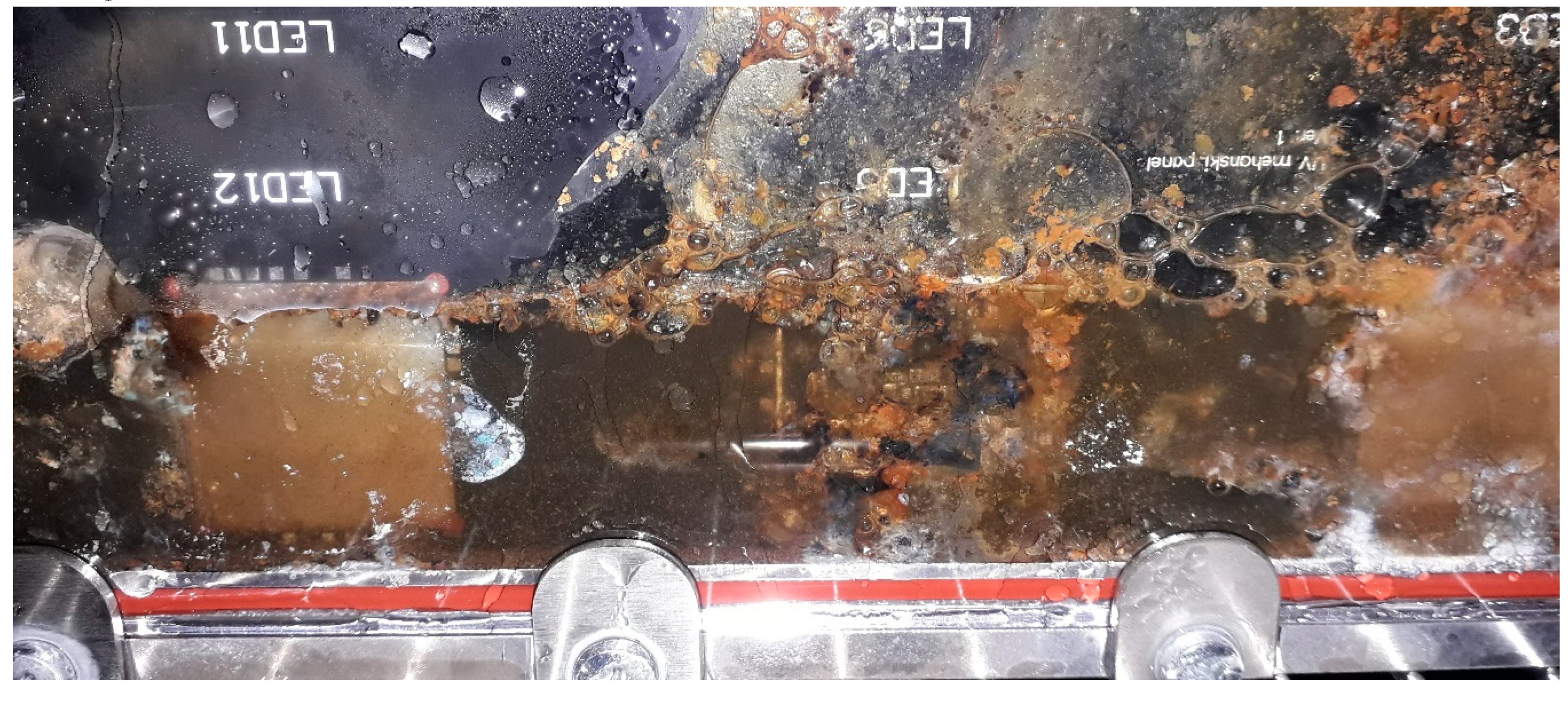
4.4. Enclosure Sealing Failure
5. Discussion
6. Conclusions
Author Contributions
Funding
Acknowledgments
Conflicts of Interest
References
- Zissis, G.; Bertoldi, P. Status of LED-Lighting World Market in 2017; European Commission, JRC: Ispra, Italy, 2018; p. 1. [Google Scholar]
- Dupuis, R.D.; Krames, M.R. History, development, and applications of high-brightness visible light-emitting diodes. J. Lightwave Technol. 2008, 26, 1154–1171. [Google Scholar] [CrossRef]
- Muramoto, Y.; Kimura, M.; Nouda, S. Development and future of ultraviolet light-emitting diodes: UV-LED will replace the UV lamp. Semicond. Sci. Technol. 2014, 29, 084004. [Google Scholar] [CrossRef]
- Schubert, E.F. Light-Emitting Diodes, 2nd ed.; Cambridge University Press: New York, NY, USA, 2006; pp. 201–236. [Google Scholar]
- Kasap, S.O. Optoelectronics and Photonics: Principles and Practices; Prentice Hall: Upper Saddle River, NJ, USA, 2001; pp. 144–145. [Google Scholar]
- Blankenbach, K.; Hertlein, F.; Hoffmann, S. Advances in automotive interior lighting concerning new LED approach and optical performance. J. Soc. Inf. Disp. 2020, 28, 655–667. [Google Scholar] [CrossRef]
- Lin, K.-H.; Huang, M.-Y.; Huang, W.-D.; Hsu, M.-H.; Yang, Z.-W.; Yang, C.-M. The effects of red, blue, and white light-emitting diodes on the growth, development, and edible quality of hydroponically grown lettuce (Lactuca sativa L. var. capitata). Sci. Hortic. 2013, 150, 86–91. [Google Scholar] [CrossRef]
- Scherff, M.L.D.; Nutter, J.; Fuss-Kailuweit, P.; Suthues, J.; Brammer, T. Spectral mismatch and solar simulator quality factor in advanced LED solar simulators. Jpn. J. Appl. Phys. 2017, 56, 08MB24. [Google Scholar] [CrossRef][Green Version]
- Matafonova, G.; Batoev, V. Recent advances in application of UV light-emitting diodes for degrading organic pollutants in water through advanced oxidation processes: A review. Water Res. 2018, 132, 177–189. [Google Scholar] [CrossRef]
- Hessling, M.; Gross, A.; Hoenes, K.; Rath, M.; Stangl, F.; Tritschler, H.; Sift, M. Efficient disinfection of tap and surface water with single high power 285 nm LED and square quartz tube. Photonics 2016, 3, 7. [Google Scholar] [CrossRef]
- Davitt, K.; Song, Y.-K.; Patterson III, W.R.; Nurmikko, A.V.; Gherasimova, M.; Han, J.; Pan, Y.-L.; Chang, R.K. 290 and 340 nm UV LED arrays for fluorescence detection from single airborne particles. Opt. Express 2005, 13, 9548. [Google Scholar] [CrossRef]
- Hubert, M.; Dimas, C.F.; Orava, P.; Koo, J. High-power UV LED array for curing photoadhesives. In Proceedings of the Applications of Photonic Technology, Quebec City, QC, Canada, 15 December 2003; pp. 163–168. [Google Scholar]
- Hölz, K.; Lietard, J.; Somoza, M.M. High-power 365 nm UV LED mercury arc lamp replacement for photochemistry and chemical photolithography. ACS Sustain. Chem. Eng. 2017, 5, 828–834. [Google Scholar] [CrossRef]
- Pirc, M.; Caserman, S.; Ferk, P.; Topič, M. Compact UV LED lamp with low heat emissions for biological research applications. Electronics 2019, 8, 343. [Google Scholar] [CrossRef]
- Moreno, I.; Avendaño-Alejo, M.; Tzonchev, R.I. Designing light-emitting diode arrays for uniform near-field irradiance. Appl. Opt. 2006, 45, 2265. [Google Scholar] [CrossRef]
- Rey-Barroso, L.; Burgos-Fernández, F.; Delpueyo, X.; Ares, M.; Royo, S.; Malvehy, J.; Puig, S.; Vilaseca, M. Visible and extended near-infrared multispectral imaging for skin cancer diagnosis. Sensors 2018, 18, 1441. [Google Scholar] [CrossRef] [PubMed]
- Błaszczak, U.J.; Gryko, Ł.; Zając, A.S. Characterization of multi-emitter tuneable led source for endoscopic applications. Metrol. Meas. Syst. 2019, 26, 153–169. [Google Scholar] [CrossRef]
- Bartczak, P.; Gebejes, A.; Falt, P.; Parkkinen, J.; Silfstein, P. Led-based spectrally tunable light source for camera characterization. In Proceedings of the 2015 Colour and Visual Computing Symposium (CVCS), Gjovik, Norway, 25–26 August 2015; pp. 1–5. [Google Scholar]
- Kagel, H.; Jacobs, H.; Bier, F.; Glökler, J.; Frohme, M. A novel microtiter plate format high power open source LED array. Photonics 2019, 6, 17. [Google Scholar] [CrossRef]
- Lei, P.; Wang, Q.; Zou, H. Designing LED array for uniform illumination based on local search algorithm. J. Eur. Opt. Soc.-Rapid 2014, 9. [Google Scholar] [CrossRef]
- Rojec, Ž. Optical Optimization of LED Array in a Solar Simulator. Master’s Thesis, University of Ljubljana, Ljubljana, Slovenia, 2014. [Google Scholar]
- Kempe, M.D. Ultraviolet light test and evaluation methods for encapsulants of photovoltaic modules. Sol. Energy Mater. Sol. Cells 2010, 94, 246–253. [Google Scholar] [CrossRef]
- Mansour, D.E.; Barretta, C.; Pitta Bauermann, L.; Oreski, G.; Schueler, A.; Philipp, D.; Gebhardt, P. Effect of Backsheet Properties on PV Encapsulant Degradation during Combined Accelerated Aging Tests. Sustainability 2020, 12, 5208. [Google Scholar] [CrossRef]
- Jošt, M.; Albrecht, S.; Kegelmann, L.; Wolff, C.M.; Lang, F.; Lipovšek, B.; Krč, J.; Korte, L.; Neher, D.; Rech, B.; et al. Efficient light management by textured nanoimprinted layers for perovskite solar cells. ACS Photonics 2017, 4, 1232–1239. [Google Scholar] [CrossRef]
- Owen-Bellini, M.; Hacke, P.; Miller, D.C.; Kempe, M.D.; Spataru, S.; Tanahashi, T.; Mitterhofer, S.; Jankovec, M.; Topič, M. Advancing reliability assessments of photovoltaic modules and materials using combined-accelerated stress testing. Prog. Photovolt. Res. Appl. 2020, in press. [Google Scholar] [CrossRef]
- Ndiaye, A.; Charki, A.; Kobi, A.; Kébé, C.M.; Ndiaye, P.A.; Sambou, V. Degradations of silicon photovoltaic modules: A literature review. Sol. Energy 2013, 96, 140–151. [Google Scholar] [CrossRef]
- Cheng, H.H.; Huang, D.-S.; Lin, M.-T. Heat dissipation design and analysis of high power LED array using the finite element method. Microelectron. Reliab. 2012, 52, 905–911. [Google Scholar] [CrossRef]
- Mitterhofer, S.; Jankovec, M.; Topič, M. A setup for in-situ measurements of potential and UV induced degradation of PV modules inside a climatic chamber. In Proceedings of the 53rd International Conference on Microelectronics, Devices and Materials MIDEM, Ljubljana, Slovenia, 4–6 October 2017; pp. 65–70. [Google Scholar]
- Mitterhofer, S.; Jankovec, M.; Topic, M. Using UV LEDs for PV module aging and degradation study. In Proceedings of the 35th European Photovoltaic Solar Energy Conference and Exhibition, Brussels, Belgium, 24–28 September 2018; pp. 1323–1327. [Google Scholar] [CrossRef]
- Wood, D. Optoelectronic Semiconductor Devices; Prentice Hall: New York, NY, USA, 1994; pp. 84–88. [Google Scholar]
- Korošak, Ž. Modularno Svetilo iz Svetlečih Diod za Osvetljevanje Fotonapetostnih Modulov. Master’s Thesis, University of Ljubljana, Ljubljana, Slovenia, 2018. [Google Scholar]
- LED Engin LZ4-04UV00 Datasheet. Available online: http://www.ledengin.com/files/products/LZ4/LZ4-04UV00.pdf (accessed on 26 February 2020).
- Hamamatsu Photonics S1087/S1133 Series Datasheet. Available online: https://www.hamamatsu.com/resources/pdf/ssd/s1087_etc_kspd1039e.pdf (accessed on 17 June 2020).
- International Electrotechnical Commission. IEC 60904-9:2020—Photovoltaic Devices—Part 9: Classification of Solar Simulator Characteristics; International Electrotechnical Commission: Geneva, Switzerland, 2020; p. 10. [Google Scholar]
Publisher’s Note: MDPI stays neutral with regard to jurisdictional claims in published maps and institutional affiliations. |


| LED # | 1 | 3 | 5 | 7 | 9 | 11 | 13 | 15 | 17 | 19 |
| Rel. Power (%) | 23.5 | 17.2 | 16.0 | 8.9 | 17.2 | 12.0 | 16.0 | 8.9 | 23.5 | 17.2 |
| Setting (0-255) | 57 | 36 | 40 | 28 | 46 | 25 | 34 | 19 | 60 | 44 |
| Relative Humidity (%) | 20 | 50 | 80 | 50 | 20 |
| Time (Days) | 1 | 10 | 7 | 7 | 7 |
| Array Temperature (°C) | 50 ± 3 | 50 ± 3 | 60 ± 3 | 60 ± 3 | 60 ± 3 |
| LED # | 1 | 3 | 5 | 7 | 9 | 11 | 13 | 15 | 17 | 19 |
| Iterative (%) | 100 | 73 | 68 | 38 | 73 | 51 | 68 | 38 | 100 | 73 |
| GA/PS (%) | 100 | 77 | 77 | 52 | 78 | 56 | 77 | 52 | 100 | 77 |
© 2020 by the authors. Licensee MDPI, Basel, Switzerland. This article is an open access article distributed under the terms and conditions of the Creative Commons Attribution (CC BY) license (http://creativecommons.org/licenses/by/4.0/).
Share and Cite
Mitterhofer, S.; Korošak, Ž.; Rojec, Ž.; Jankovec, M.; Topič, M. Development and Analysis of a Modular LED Array Light Source. Photonics 2020, 7, 92. https://doi.org/10.3390/photonics7040092
Mitterhofer S, Korošak Ž, Rojec Ž, Jankovec M, Topič M. Development and Analysis of a Modular LED Array Light Source. Photonics. 2020; 7(4):92. https://doi.org/10.3390/photonics7040092
Chicago/Turabian StyleMitterhofer, Stefan, Žiga Korošak, Žiga Rojec, Marko Jankovec, and Marko Topič. 2020. "Development and Analysis of a Modular LED Array Light Source" Photonics 7, no. 4: 92. https://doi.org/10.3390/photonics7040092
APA StyleMitterhofer, S., Korošak, Ž., Rojec, Ž., Jankovec, M., & Topič, M. (2020). Development and Analysis of a Modular LED Array Light Source. Photonics, 7(4), 92. https://doi.org/10.3390/photonics7040092