Article

Irregular Shifting of RF Driving Signal Phase to Overcome Dispersion Power Fading

Department of Electrical Engineering, Universitas Indonesia, Jawa Barat 16424, Indonesia
*
Author to whom correspondence should be addressed.
Photonics 2019, 6(4), 104; https://doi.org/10.3390/photonics6040104
Submission received: 5 September 2019 / Revised: 2 October 2019 / Accepted: 9 October 2019 / Published: 12 October 2019

Abstract

:
The main problem with the radio-over-fiber (RoF) link is the decrease in the recovered radio frequency (RF) power due to the chromatic dispersion of the fiber known as dispersion power fading. One of the methods for dealing with dispersion power fading is to use the optical single sideband (OSSB) modulation scheme. The OSSB modulation scheme can be generated by biasing the dual-drive Mach–Zehnder modulator (DD-MZM) to the quadrature bias point (QBP) and shifting the RF drive signal phase (θ) by 90°, which is called the regular θ. However, the OSSB modulation scheme only overcomes dispersion power fading well at the modulation index (m) < 0.2. This paper proposes an irregular θ method to overcome dispersion power fading at all m. There are two irregular θ for every m used. The irregular θ managed to handle dispersion power fading better than OSSB modulation scheme did at every m. Specifically, the irregular θ could handle the dispersion power fading well at m ≤ 1. In sum, the irregular θ could overcome the dispersion power fading at any RF frequency and optical wavelength without having to re-adjust the transmitter.

1. Introduction

A radio-over-fiber (RoF) system transmits radio frequency (RF) (XTX(t)) signals through optical fiber used to support wireless communication services. The XTX(t) in the RoF system is converted to an optical signal using an electro-optic (E/O) converter located at the central office (CO). The optical signal is later transmitted through a fiber link, and the RF signal is recovered using an opto-electric (O/E) converter positioned on the radio access point (RAP). The recovered RF signal (Xrec(t)) is then transmitted wirelessly from the RAP to mobile station (MS). It is possible to convert RF signal to the optical one by modulating the optical source directly or externally, both of which serve as intensity modulation (IM) or phase modulation (PM). The intensity modulation is used most commonly because it has a simple system. Recovering RF signal can be done by direct detection (DD) using a photodetector [1].
IM on the RoF system produces modulated light waves (ETX(t)) with double-sideband spectrum (double-sideband optical modulation, henceforth ODSB). When the ODSB signal is transmitted through a fiber link, the chromatic dispersion of the fiber causes the sideband and optical carrier to propagate at different speeds. This leads the modulated signal at the receiver (ERX(t)) to experience a phase difference between the sideband and optical carrier by φ. The proportion of φ follows the length of the fiber (L), the frequency of the RF signal (fm) and the wavelength (λc) used. The phase difference causes the O/E process to generate two identical RF signals but with a different phase of 2φ, resulting in constructive and destructive interference on Xrec(t). The destructive interference reduces the power of the recovered RF signal (Prec(t)), which is known as dispersion power fading. If φ = π, massive decrease in power will occur (deep fade). The proportion of power decrease is obtained by comparing the signal power with and without the fiber, something that is known as the carrier-to-noise (C/N) penalty [2].
There are two types of light sources commonly used in RoF links, namely optical frequency comb (OFC) and single-mode laser. Chromatic dispersion fiber will give different effects on each light source. The effect of chromatic dispersion on RoF links using OFC light sources can be overcome by several methods. In [3], power fading is overcome by utilizing chromatic dispersion. The effect of chromatic dispersion on RoF links using the mode-locked laser diodes (MLLD) can be reduced using an unbalanced Mach–Zehnder interferometer (UMZI) [4], whereas in [5], the effect of chromatic dispersion is reduced by adjusting the MLLD parameters appropriately.
The focus of this paper is to overcome dispersion power fading on RoF links using a single-mode laser as a light source. The most useful method for dealing with dispersion power fading is to use spools of dispersion compensation fiber (DCF) [6]. The dispersion of DCF is negative, so by inserting DCF into the ROF link, the average dispersion is close to zero. The weakness of this method is that DCF must always be adjusted to the L used.
Dispersion power fading can also be overcome by carrier phase-shifted (CPS) method [7,8,9,10,11,12]. In this method, the optical carrier phase before transmission is arranged in such a way that φ becomes zero after transmission. With this method, the Xrec(t) is always in a constructive condition. However, the optical carrier phase before transmission should always be adjusted to the used L, fm, and λc since the proportion of φ accords with L, fm, and λc. In addition, successfully adjusting the optical carrier phase requires complex transmitter circuits.
Another feasible method is using the optical carrier-suppressed (OCS) modulation scheme [13,14,15,16,17,18,19,20]. With the OCS modulation, the optical carrier is removed so that ETX(t) consists only of upper and lower sidebands. The Xrec(t) is thus generated only from the multiplication between the upper and lower sidebands, so no interference resulting in dispersion power fading is possible. The disadvantage of this method is that the Xrec(t) frequency is twice the XTX(t) frequency, so the receiver has to do additional works to turn the Xrec(t) frequency to its original frequency.
It is also possible to deal with dispersion power fading by using an optical single-sideband (OSSB) modulation scheme [13,15,16,19,20,21,22,23,24,25,26,27,28,29,30,31,32,33,34,35,36,37,38,39,40,41,42,43] that has a spectrum consisting only of optical carriers and one sideband (either upper or lower sideband). This modulation scheme allows the Xrec(t) to have the same frequency as that of XTX(t), so it is not necessary for the receiver to adjust the Xrec(t) frequency. The OSSB modulation scheme can be generated by biasing the dual-drive Mach–Zehnder modulator (DD-MZM) on the quadrature bias point (QBP) and at the phase difference of RF drive signal (θ) = 90° [19,30,40,43,44]. The DD-MZM is an electro-optic (E/O) converter that is commonly used on RoF links. The OSSB generated using DD-MZM manages to effectively overcome dispersion power fading if the XTX(t) spectrum is made up only of optical carriers and sideband fundamentals without harmonics. Otherwise, the phase shift occurring in the harmonics may result in a decrease of the Xrec(t) power. To produce XTX(t) without harmonics, the DD-MZM must be operated at a modulation index (m) < 0.2. Hence, this method cannot overcome dispersion power fading efficiently at m ≥ 0.2.
Our previous study [45] has successfully demonstrated that modifying θ of DD-MZM biased on QBP can change the XTX(t) spectrum. Different spectrum will also produce a different level of dispersion power fading. This paper proposes, as an update, the use of irregular θ to overcome dispersion power fading. The irregular θ is a θ that produces a minimum level of dispersion power fading, which is measured using (C/N) deviation factor. To calculate the (C/N) deviation factor, it is necessary, at first, to model the recovered RF signal’s power.
The complete contribution of this paper includes:
  • A new method for dealing with dispersion power fading by using irregular θ.
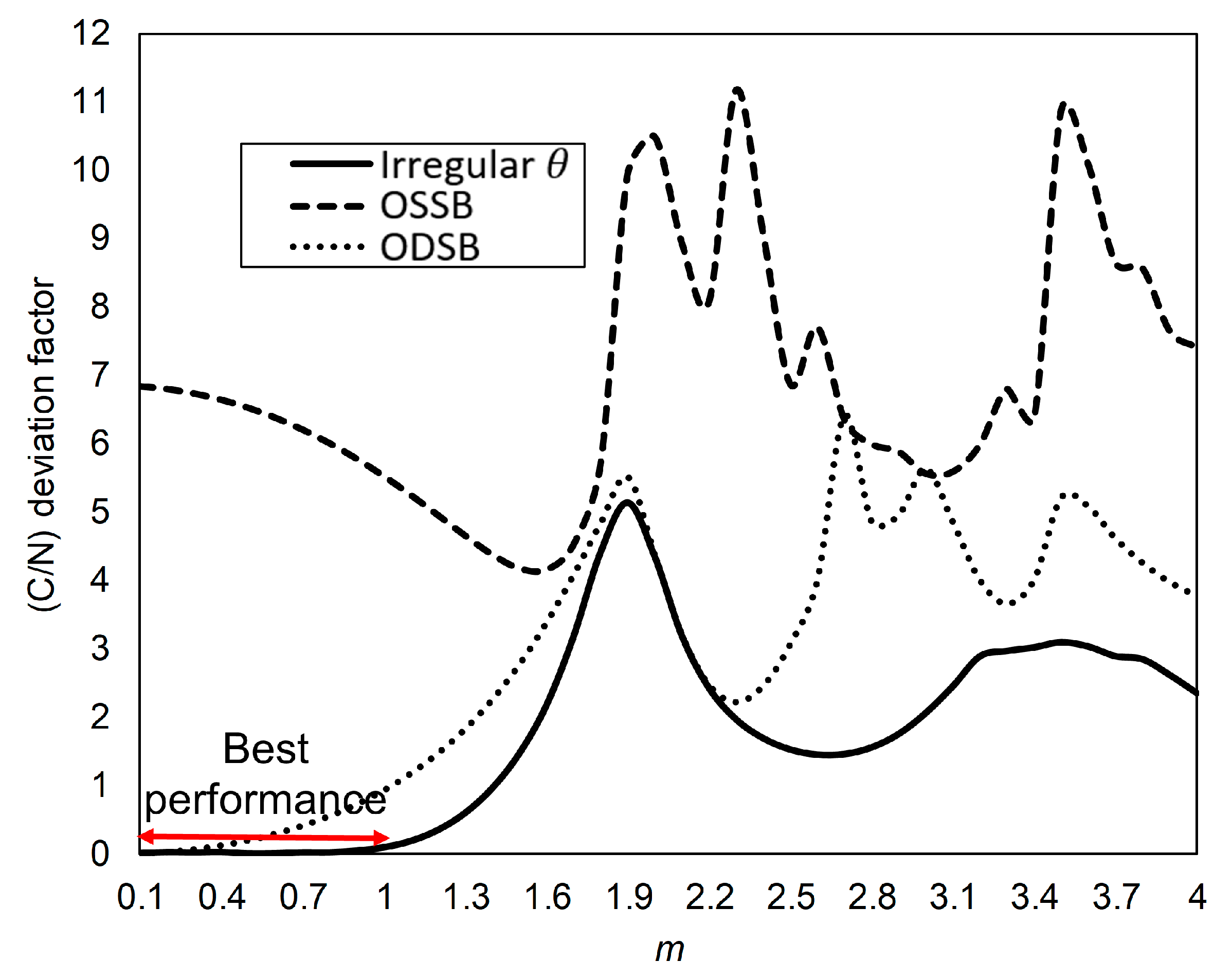
  • Generating a simple RoF link with standard DD-MZM as an E/O converter that can overcome dispersion power fading at all m. This link:
    (a)
    Can be used in any fm, L, and λc without having to re-adjust the transmitter.
    (b)
    Has Xrec(t) set at the same frequency as that of XTX(t), thereby removing any additional work.

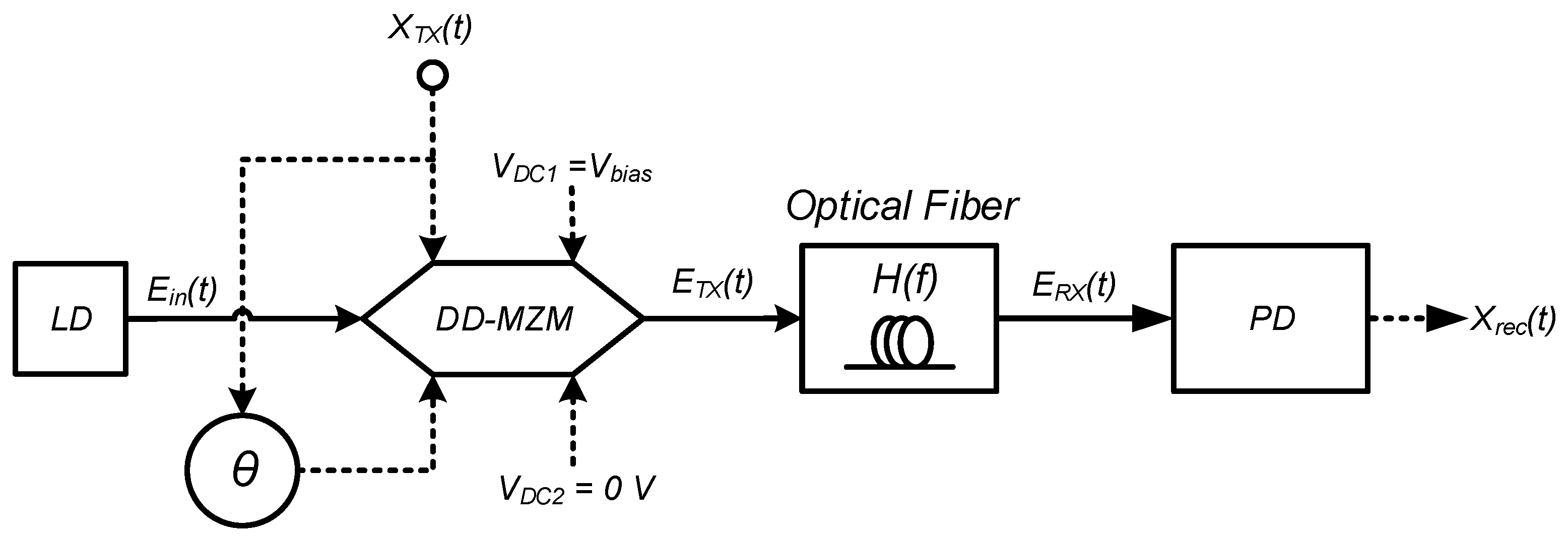
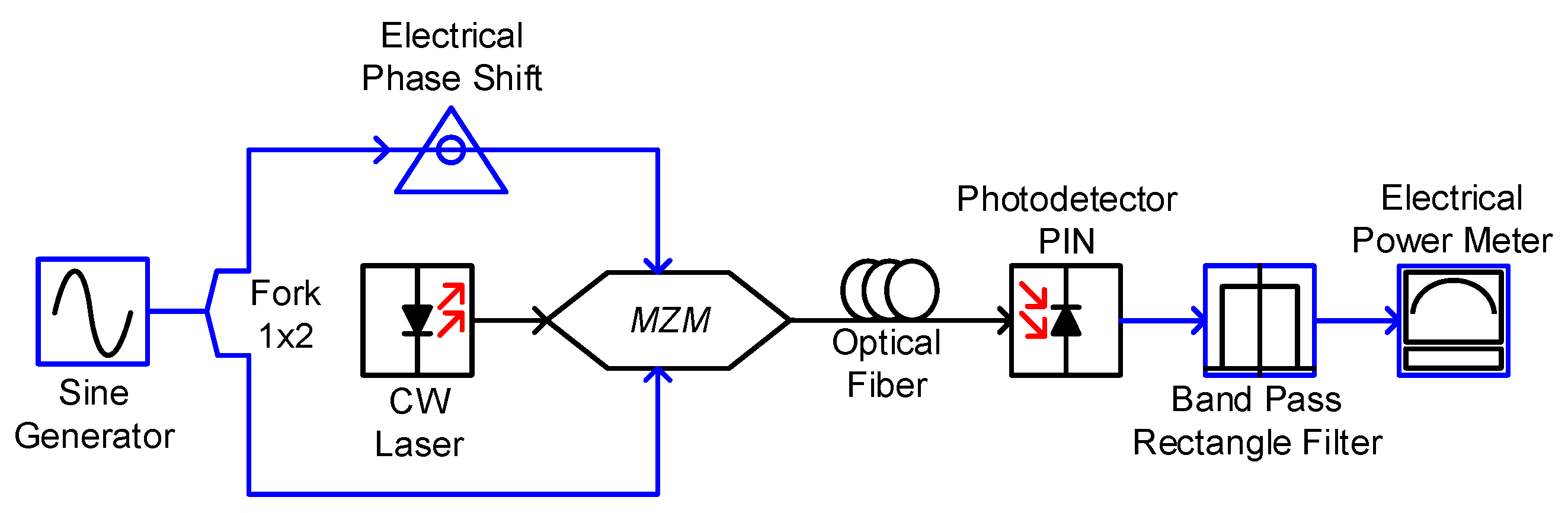
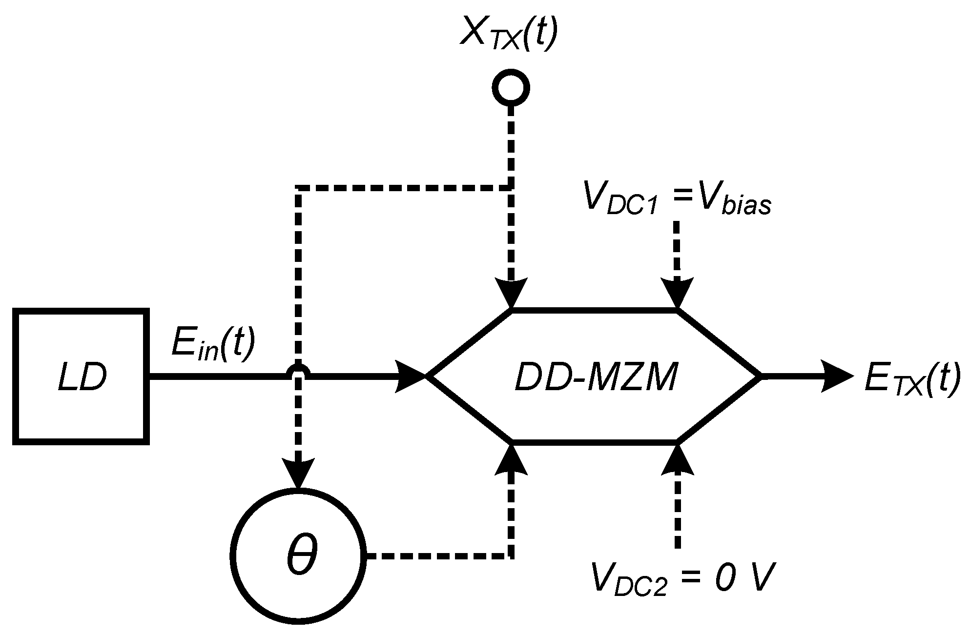
2. Principles of DD-MZM
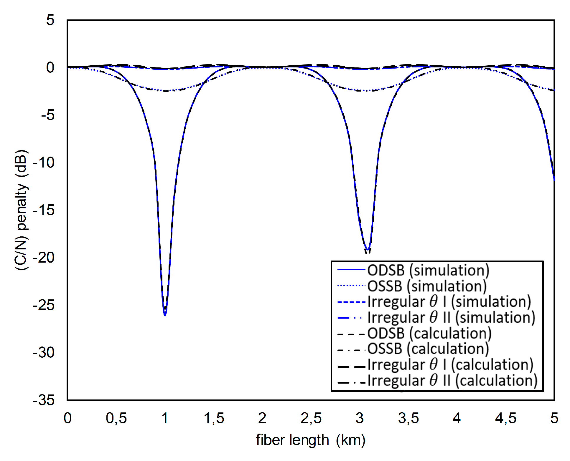
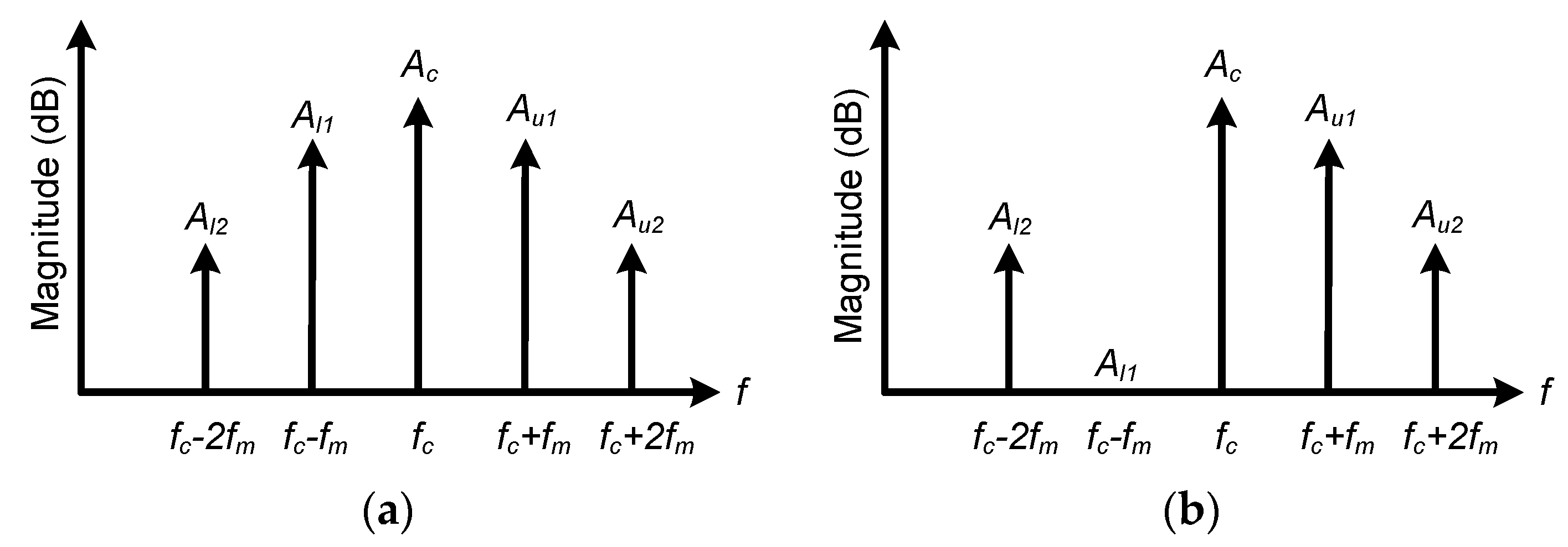
The Mach–Zehnder modulator (MZM) is an external intensity modulator commonly used on optical fiber links. It has two variants, namely single drive (SD-MZM) and dual drive (DD-MZM). The latter has two signal driver ports and two bias ports (up and down) that can be controlled independently to produce a number of different forms of optical modulation. The general configuration of DD-MZM is shown in Figure 1 in which the path is distinguished by solid and dashed lines. The dashed lines represent the path passed by the electrical domain signal, while the solid one is passed by the optical domain signal. The continuous optical wave (Ein(t)) produced by the laser diode (LD) is modulated by the RF signal (XTX(t)) to be transmitted later. The modulation is carried out by inserting XTX(t) into the upper and lower signal driver ports whose phases are differentiated using an electrical phase shifter (EPS) by θ. The upper bias port is given a Vbias voltage, while the lower one is given 0 V voltage. The modulator output optical field is expressed as ETX(t).
Ein(t) and XTX(t) are expressed in the following formula:
E i n ( t ) = E o e j 2 π f c t
X T X ( t ) = V m cos 2 π f m t ,
where Eo represents continuous optical wave amplitude, fc the continuous optical wave frequency, Vm the amplitude of the RF signal, and fm the frequency of the RF signal. As such, the upper (Vup(t)) and lower (Vdown(t)) driving signals of DD-MZM are expressed:
V u p ( t ) = V m cos ( 2 π f m t ) + V b i a s
V d o w n ( t ) = V m cos ( 2 π f m t + θ ) ,
where θ is the phase of the electrical phase shifter (EPS). Assuming that the extinction ratio (ER) of DD-MZM is extremely high, the optical field generated from DD-MZM (ETX(t)) can be approximated by the equation
E T X ( t ) 1 2 E i n ( t ) { e ( j π V u p ( t ) V π ) + e ( j π V d o w n ( t ) V π ) } ,
provided Vπ is the switching voltage of MZM. By inserting the Equations (3) and (4) into (5), the following formula is obtained
E T X ( t ) 1 2 E i n ( t ) { e ( j π V m V π cos ( 2 π f m t ) + j π V b i a s V π ) + e ( j π V m V π cos ( 2 π f m t + θ ) ) } ,
For simplicity, the Equation (6) can be stated as
E T X ( t ) = 1 2 E i n ( t ) { e ( j m cos ( 2 π f m t ) + j π γ ) + e j m cos ( 2 π f m t + θ ) } E T X ( t ) = 1 2 E i n ( t ) . { e j m cos ( 2 π f m t ) e j π γ + e j m cos ( 2 π f m t + θ ) } ,
where m = π V m V π is the DD-MZM modulation index, and γ = V b i a s V π is the normalized bias voltage.
To facilitate the analysis, the Equation (7) is written as
E T X ( t ) = 1 2 E i n ( t ) { A · e ( j π γ ) + B } ,
with
A = e j m cos ( 2 π f m t )
B = e j m cos ( 2 π f m t + θ ) ,
By implementing Jacobi–Anger expansion [46], where
e j m cos x = n = j n J n ( m ) e j n x
e j m sin x = n = J n ( m ) e j n x ,
the Equations (9) and (10) become
A = n = j n · J n ( m ) · e j n ( 2 π f m t ) ,
B = n = j n · J n ( m ) · e j n ( 2 π f m t + θ ) ,
with Jn(m) is the nth Bessel function of the first kind. Therefore, Equation (7) can be expressed as
E T X ( t ) = 1 2 E i n ( t ) { n = j n · J n ( m ) · e j n ( 2 π f m t ) · e j π γ + n = j n · J n ( m ) · e j n ( 2 π f m t + θ ) } E T X ( t ) = 1 2 E i n ( t ) { n = j n · J n ( m ) · ( e j n ( 2 π f m t ) · e j π γ + e j n ( 2 π f m t ) · e j n θ ) } E T X ( t ) = 1 2 E i n ( t ) { n = j n · ( e j π γ + e j n θ ) · J n ( m ) · e j n 2 π f m t } ,
By inserting (1) into (15), it is obtained
E T X ( t ) = 1 2 E o e j 2 π f c t { n = j n · ( e j π γ + e j n θ ) · J n ( m ) · e j n 2 π f m t } E T X ( t ) = 1 2 E o { n = j n · ( e j π γ + e j n θ ) · J n ( m ) · e j 2 π ( f c + n f m ) t } .
It is noticeable from Equation (16) that the optical field generated from DD-MZM consists of an optical carrier and sideband with infinite order. In accordance with the Bessel function, the formed sideband order is influenced by the m used. The greater the m, the more the sideband orders formed.
By adjusting parameters γ and θ in Equation (16), the following modulation schemes will be obtained:
  • For θ = 180 o and γ = 1 2 (QBP, which is V b i a s = 1 2 V π ), an ODSB modulation scheme is produced. The spectrum of this modulated signal is shown in Figure 2a.
  • For θ = 90 o and γ = 1 2 , an OSSB modulation scheme is produced. In this instance, only (4n + 1) order lower sidebands are suppressed, where n is an integer [19]. The spectrum can be seen in Figure 2b.

3. Modeling of Recovered RF Signal Power

To calculate the (C/N) deviation factor, it is necessary to first model the recovered RF signal’s power. Power modeling is carried out for the RoF link consisting of DD-MZM as an E/O converter; optical fiber, which is dispersive with H(f) response; and photodetector (PD), which is an O/E converter as shown in Figure 3.
To simplify the analysis, the Equation (16) can be rewritten as
E T X ( t ) = A c e j 2 π f c t + n = 1 { A l n e j 2 π ( f c n f m ) t + A u n e j 2 π ( f c + n f m ) t } ,
where
A c = 1 2 E o ( e j π γ + 1 ) · J 0 ( m ) A l n = 1 2 E o j n ( e j π γ + e j n θ ) · J n ( m ) A u n = 1 2 E o j n ( e j π γ + e j n θ ) · J n ( m ) .
The function of dispersive fiber link transfer is obtained from [47]
H ( f ) = e j D L λ c 2 ( f f c ) 2 c ,
where D is the chromatic dispersion in ps/(nm km), λc the optical wavelength, f the frequency offset of the optical carrier, c the speed of light in vacuum, and L the fiber length in km. When ETX(t) is transmitted through a dispersive link, a phase difference occurs between the first-order sideband and the optical carrier
ϕ = D L λ c 2 f m 2 c ,
while the phase difference between the optical carrier and any sideband is the square of the frequency range ( ± n f m ) ,   which   is given by [48]
ϕ n = n 2 ϕ ,
Thus, the optical field that arrives at the receiver end (ERX(t)) is formulated below:
E R X ( t ) = A c e j 2 π f c t + n = 1 { A l n e j 2 π ( f c n f m ) t + A u n e j 2 π ( f c + n f m ) t } · e j n 2 ϕ ,
At the receiver end, the ERX(t) is detected using a photodetector which is a squared-envelope operator, given by [2]
| E R X ( t ) | 2 = E R X ( t ) · E R X * ( t ) ,
by simply taking the fm term, it is obtained
| E R X ( t ) | 2 = e j 2 π f m t { A c A l 1 * e j ϕ + A c * A u 1 e j ϕ + A l 1 A l 2 * e j 3 ϕ + A u 1 * A u 2 e j 3 ϕ + A l 2 A l 3 * e j 5 ϕ + A u 2 * A u 3 e j 5 ϕ + } | E R X ( t ) | 2 = e j 2 π f m t { n = 0 ( A l n A l ( n + 1 ) * e j ( 2 n + 1 ) ϕ + A u n * A u ( n + 1 ) e j ( 2 n + 1 ) ϕ ) } ,
where A l 0 = A u 0 = A c .
The real portion of Equation (23) is equivalent to the photodetector’s output current and is equal to Xrec(t) [47], so
X r e c ( t ) { n = 0 ( A l n A l ( n + 1 ) * e j ( 2 n + 1 ) ϕ + A u n * A u ( n + 1 ) e j ( 2 n + 1 ) ϕ ) } cos 2 π f m t .
The square of the amplitude term in the Equation (24) is the Xrec(t) power [2], so the formula below is used to measure the power of the recovered RF signal as a function of L
P r e c ( L ) = { n = 0 ( A l n A l ( n + 1 ) * e j ( 2 n + 1 ) ϕ + A u n * A u ( n + 1 ) e j ( 2 n + 1 ) ϕ ) } 2 ,
with
ϕ = D L λ c 2 f m 2 c , A l n * = 1 2 E o ( j n ) ( e j π γ + e j n θ ) · J n ( m ) ,  
and
A u n * = 1 2 E o ( j n ) ( e j π γ + e j n θ ) · J n ( m ) .
The recovered RF signal is obtained from the multiplication of nth order lower sideband with (n + 1)th order conjugated lower sideband plus the multiplication of nth order conjugated upper sideband with (n + 1)th order upper sideband, where n is an integer. The recovered RF signal power is obtained by squaring the amplitude of the signal.
The extent to which the power of the recovered RF signal decreases due to fiber dispersion is known as a (C/N) penalty, which is calculated by comparing Prec(L) with and without fiber transmission. The calculation is mathematically stated as [2]
( C / N ) p e n a l t y = 10 log | P r e c ( L ) w i t h f i b e r P r e c ( L ) w i t h o u t f i b e r | .
This paper puts forward the idea of using (C/N) deviation factor to measure the dispersion power fading level satisfying the following equation:
( C / N ) d e v i a t i o n f a c t o r = i = 0 N ( ( C / N ) p e n a l t y ( i )     ( C / N ) p e n a l t y ¯ ) 2 N .
Note: The ( C / N ) p e n a l t y ( i ) is the i-sample of (C/N) penalty, ( C / N ) p e n a l t y ¯ is the average sample of (C/N) penalty, and N is the number of samples. The lower the (C/N) deviation factor, the smaller the effect of dispersion on Prec(L). The minimum sample required for this calculation is one deep fade cycle, as shown in Figure 4a.

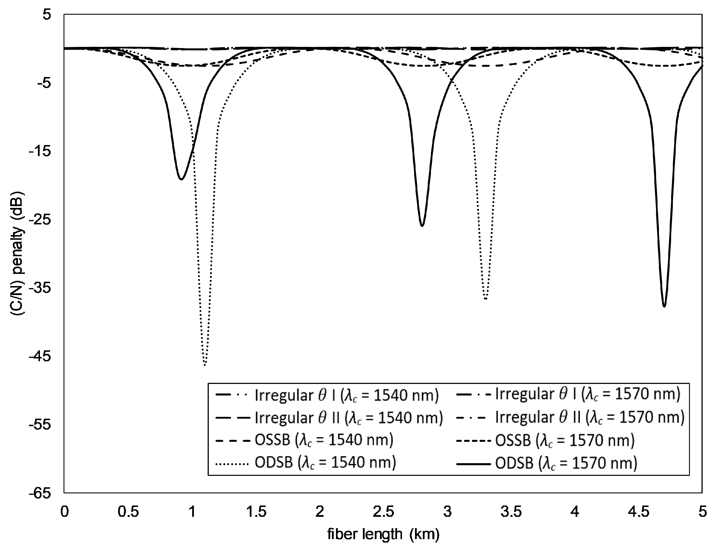
3.1. (C/N) Penalty on ODSB

The modulation scheme commonly used on RoF links is optical double sideband (ODSB). The RoF link with DD-MZM as E/O converter will produce an ODSB modulation scheme if DD-MZM is biased to QBP and the degree of RF phase shifting (θ) equals 180°. The calculation of (C/N) penalty on the RoF link with ODSB modulation follows (26) by calculating Prec(L) from the Equation (25), where Prec(L) without fiber = Prec(0), and (C/N) penalty (dB) = Prec(L) (dBm) − Prec(0) (dBm). The parameters used in this calculation are λc = 1550 nm with D = 17 ps/(nm.km), and fm = 60 GHz. The range of fiber length L is 0 to 5 km with a step of 0.1 km. The calculations are made at m = 0.1, 0.5, 0.8, 1, 1.5, 2, 3, and 4. According to Bessel function, Jn(4) is still significant until n = 10. Thus, the considered sideband in this calculation is that reaching until the 10th order (n = 10). The (C/N) penalty curve as the result of the calculation is shown in Figure 4.
The vertical axis in Figure 4 expresses the (C/N) penalty in dB, and the horizontal axis expresses the fiber length in km. Figure 4a shows the (C/N) penalty curve at m ≤ 1, while Figure 4b is the (C/N) penalty curve at m > 1. It is obvious from Figure 4a that the RoF link with ODSB modulation at all m experiences deep fade (large power loss) at L = 1 and 3.1 km. Based on the Equation (26), the value of (C/N) deviation factor of RoF link with ODSB modulation is 6.8 at m = 0.1, 6.5 at m = 0.5, 6.0 at m = 0.8, and 5.5 at m = 1. The values indicate that the smaller the m, the larger the (C/N) deviation factor of RoF link with ODSB modulation. In other words, smaller m values make the RoF link with ODSB modulation increasingly affected by dispersion. As shown in Figure 4b, the RoF link at m > 1 experiences deep fade at the various length of the fiber and has an irregular pattern. The same case happens with the (C/N) deviation factor at m > 1, which is 4.1 at m = 1.5, 10.5 at m = 2, 5.6 at m = 3, and 7.4 at m = 4.
To find out the effect of dispersion on the RoF link at different fm, the researchers did a calculation of (C/N) penalty with m = 1, λc = 1550 nm, D = 17 ps/(nm km) at L = 1 km to 5 km with a step of 0.1 km. The fm was varied at 30, 40, 50, 60, and 70 GHz. The results are shown in Figure 5a. On the other hand, to establish the effect of dispersion to the RoF link at different λc, the researchers made a similar (C/N) penalty calculation at m = 1, fm = 60 GHz, at L = 1 km to 5 km with a step of 0.1 km. The λc was also varied at 1540 nm (D = 16 ps/(nm km)), 1550 nm (D = 17 ps/(nm km)), 1560 nm (D = 17.5 ps/(nm km)), and 1570 nm (D = 18 ps/(nm km)), and the results of the calculation are given in Figure 5b. On the RoF link with variation fm, the bigger the fm used, the closer the distance of the deep fade. Likewise, on the RoF link with variation λc, bigger λc results in a closer distance of the deep fade.

3.2. (C/N) Penalty on OSSB

One method used to manage the (C/N) penalty is the OSSB modulation scheme. The RoF link with DD-MZM as the E/O converter will produce an OSSB modulation scheme if DD-MZM is biased to QBP and θ is set to 90° [19,30,40,43,44]. To see the (C/N) penalty of RoF link with OSSB modulation, the same calculation as that on ODSB is done but with θ set to 90°. The results of (C/N) penalty from this calculation are shown in Figure 6.
Figure 6a displays (C/N) penalty curve on the RoF link with OSSB modulation at m ≤ 1. At this value of m, no deep fade was recorded, unlike that with ODSB modulation, but there remained a decrease of power by 0.6 dB at m = 0.5, 1.5 dB at m = 0.8, and 2.5 dB at m = 1. In other words, the greater the m used, the greater the decrease of power. The power reduction did not occur at m = 0.1, which means that the OSSB modulation scheme can only overcome the (C/N) penalty at m = 0.1. The value of (C/N) deviation factor of RoF link with OSSB modulation is 0.9 at m = 1, 0.6 at m = 0.8, 0.2 at m = 0.5, and 0.0 at m = 0.1. Hence, the RoF link with the OSSB modulation scheme is not, by implication, affected by the dispersion at m = 0.1—the larger the m, the greater the effect of dispersion on the recovered RF signal power. What the curve of (C/N) penalty and the (C/N) deviation factor show is that the OSSB modulation scheme cannot effectively overcome dispersion power fading at m > 0.1.
The image of (C/N) penalty curve on the RoF link with OSSB modulation at m > 1 is given in Figure 6b. It is visible at this level of m that the OSSB modulation scheme is no longer capable of overcoming dispersion power fading, which is marked by the significant loss of power at every use. Figure 6c,d is (C/N) penalty curve on the RoF link with OSSB modulation at various fm and λc respectively. The curve was obtained from calculations with m = 1, λc = 1550 nm, and D = 17 ps/(nm km). Both figures illustrate the loss of power by 2.5 dB at different fiber length for different fm and λc. This implies that the OSSB modulation scheme is also unable to overcome dispersion power fading effectively at other fm and λc for m > 0.1.

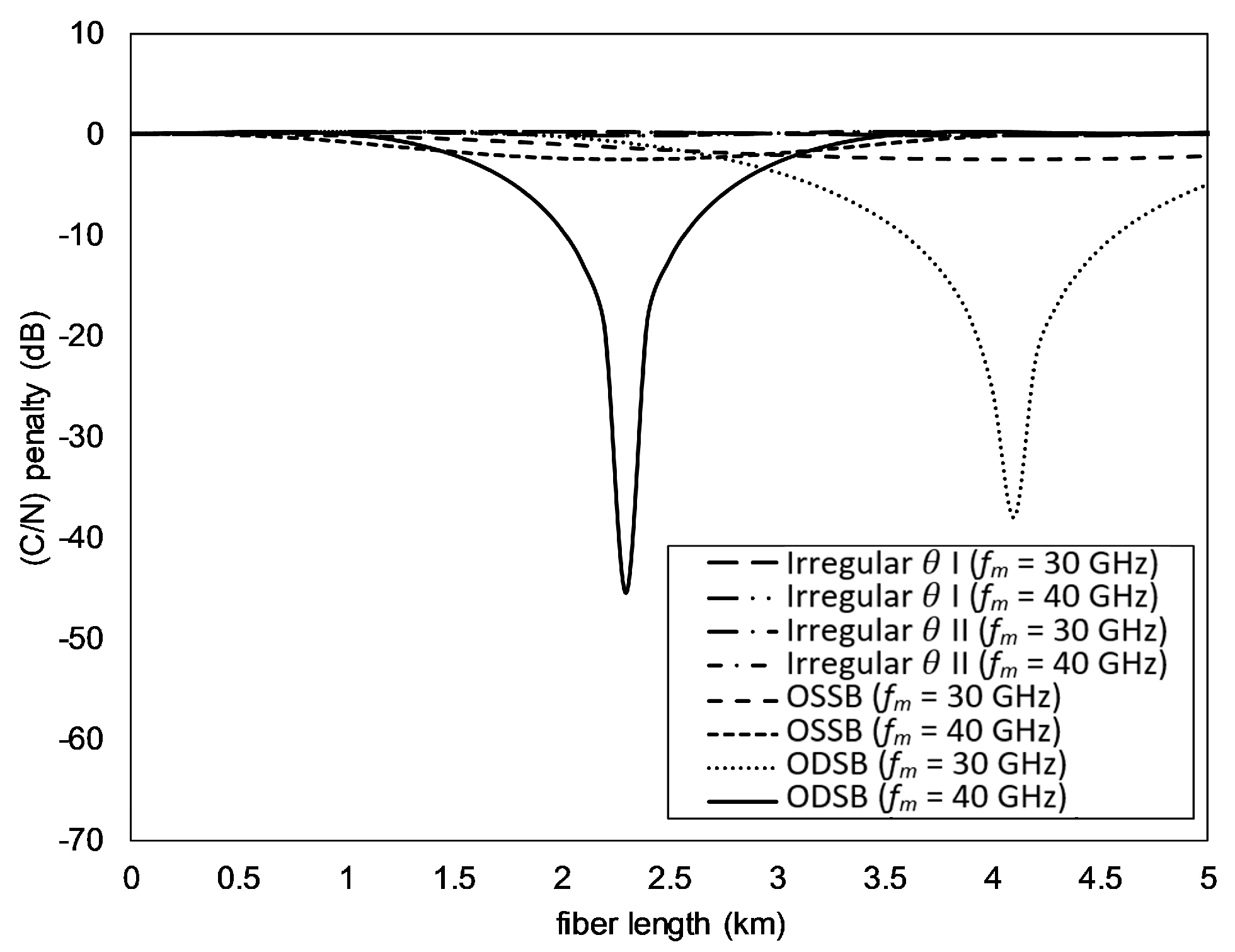
4. Irregular Phase Shifted

Our previous research [45] proved that altering θ on the RoF link with DD-MZM biased in QBP causes the XTX(t) spectrum to change as well. The XTX(t) with a different spectrum will result in a different (C/N) deviation factor. The proper shape of the spectrum will produce a small (C/N) deviation factor value, so choosing the right irregular θ will produce a minimum (C/N) deviation factor value.
The search for irregular θ is performed for γ = ½ with the following steps:
(a)
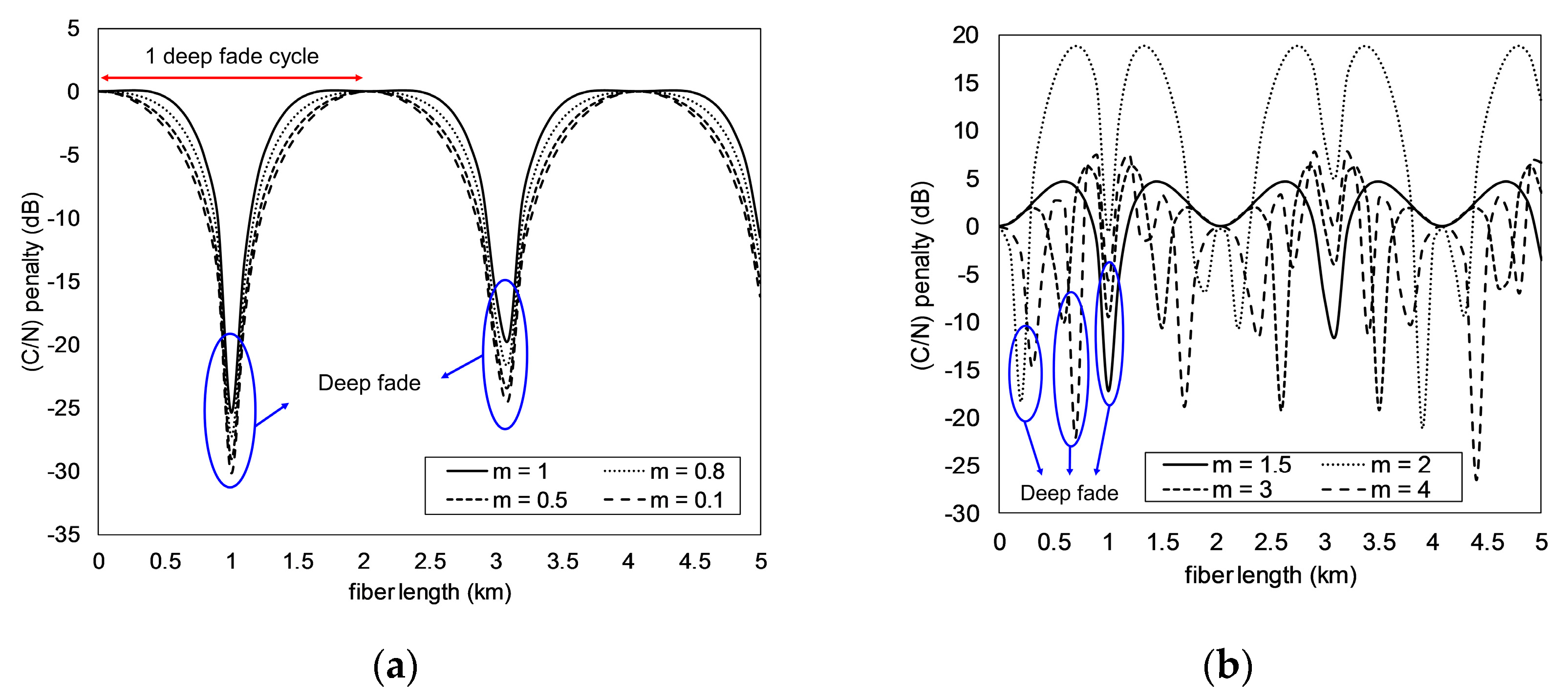
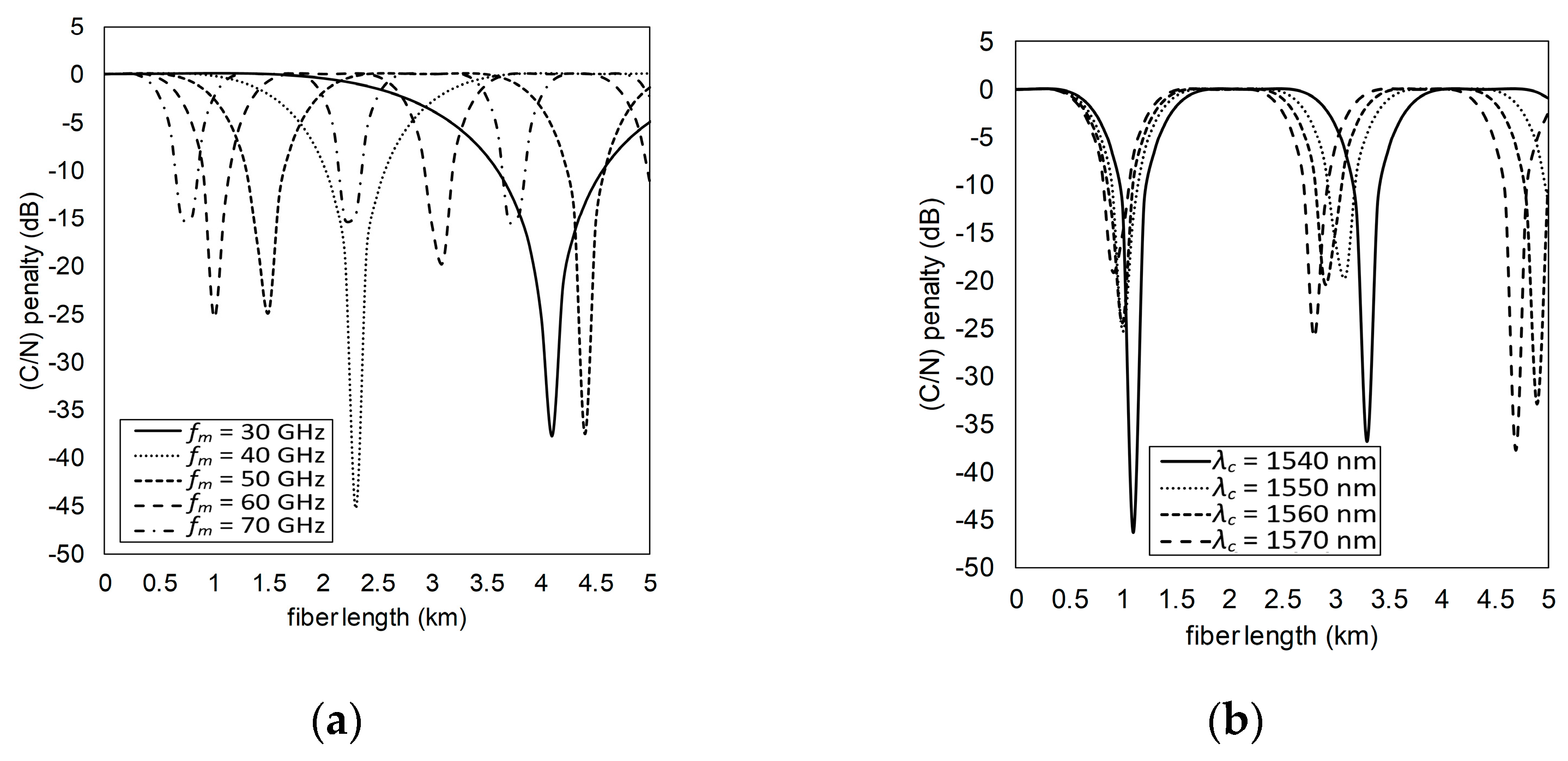
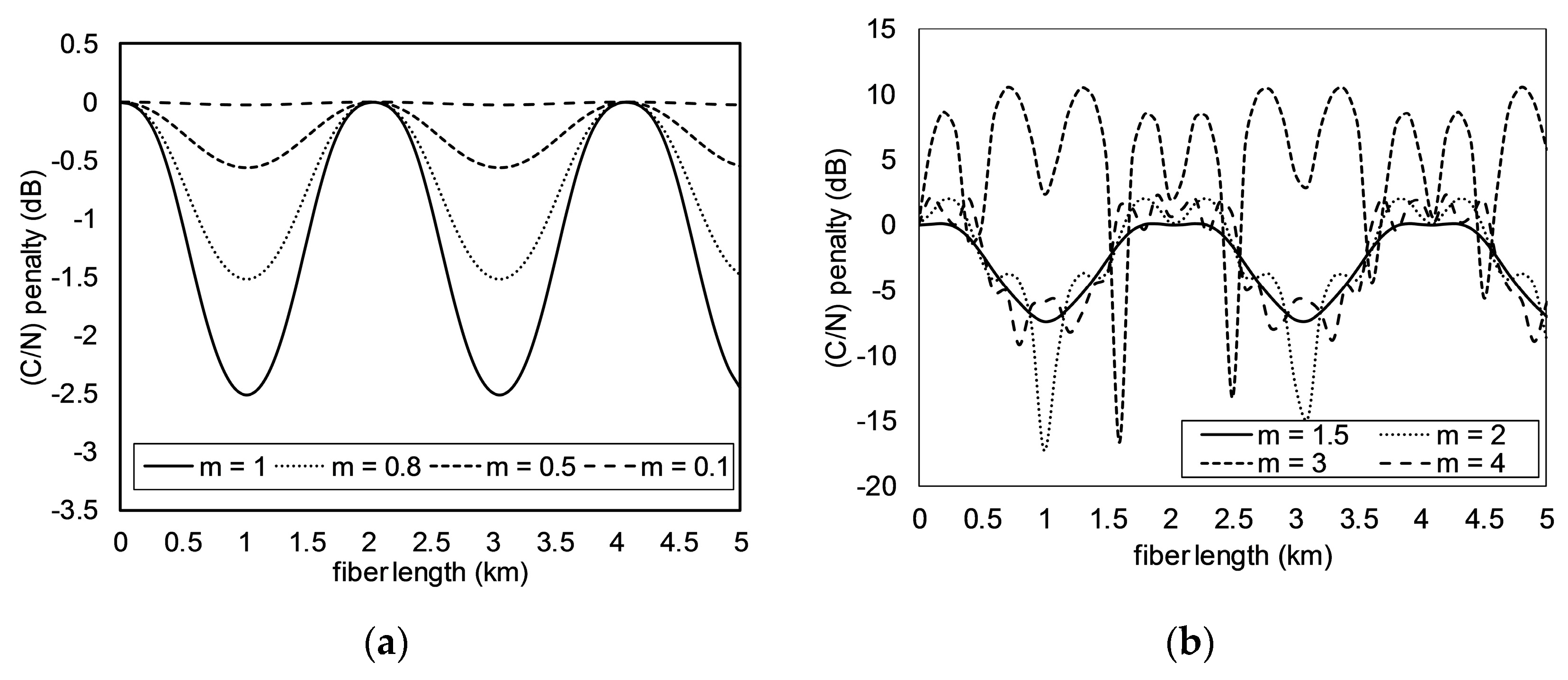
Calculate Prec(L) using (24) with n = 10, m = 0.1, θ = 0 rad, λc = 1550 nm (D = 17 ps/(nm km)), and fm = 60 GHz. The Prec(L) is calculated at 0 ≤ L ≤ 5 km with step 0.1 km.
(b)
From the obtained Prec(L) in a), calculate the (C/N) penalty using (26).
(c)
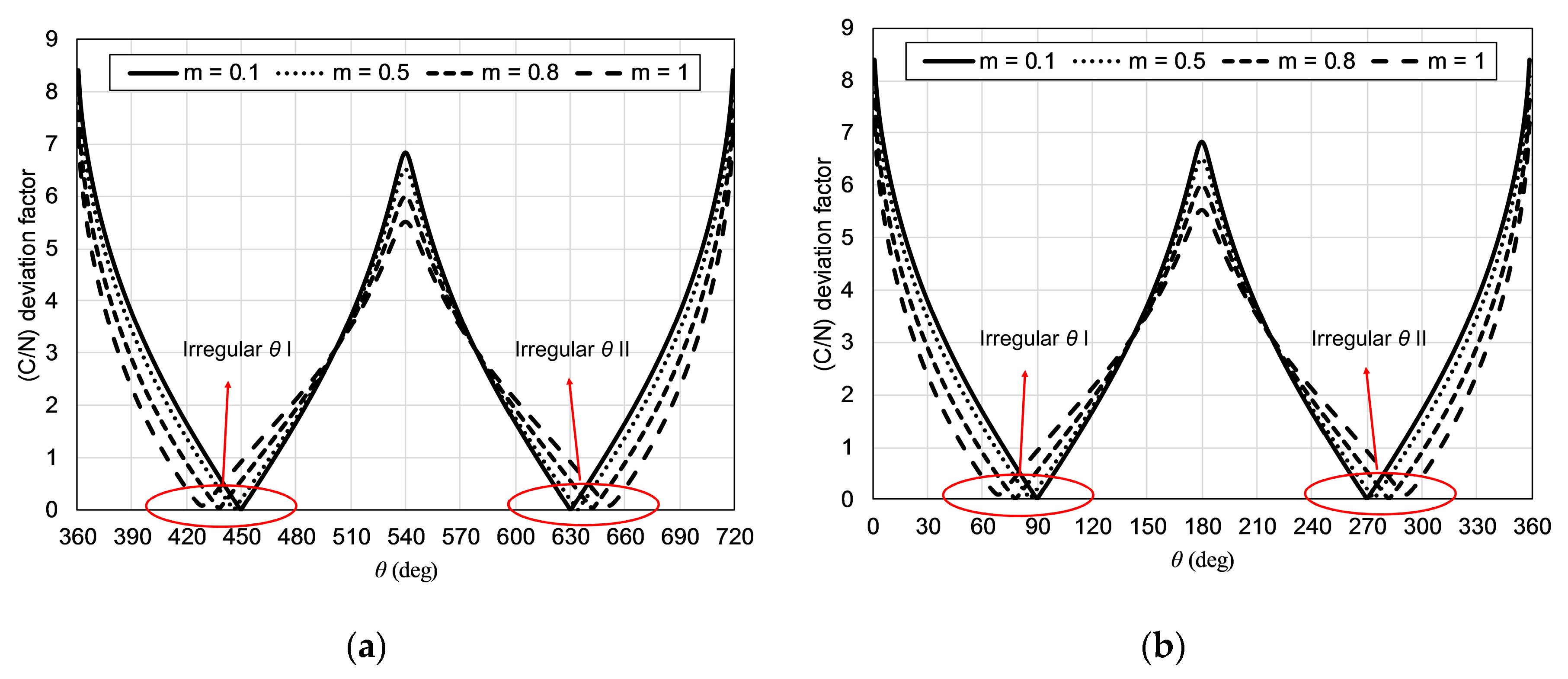
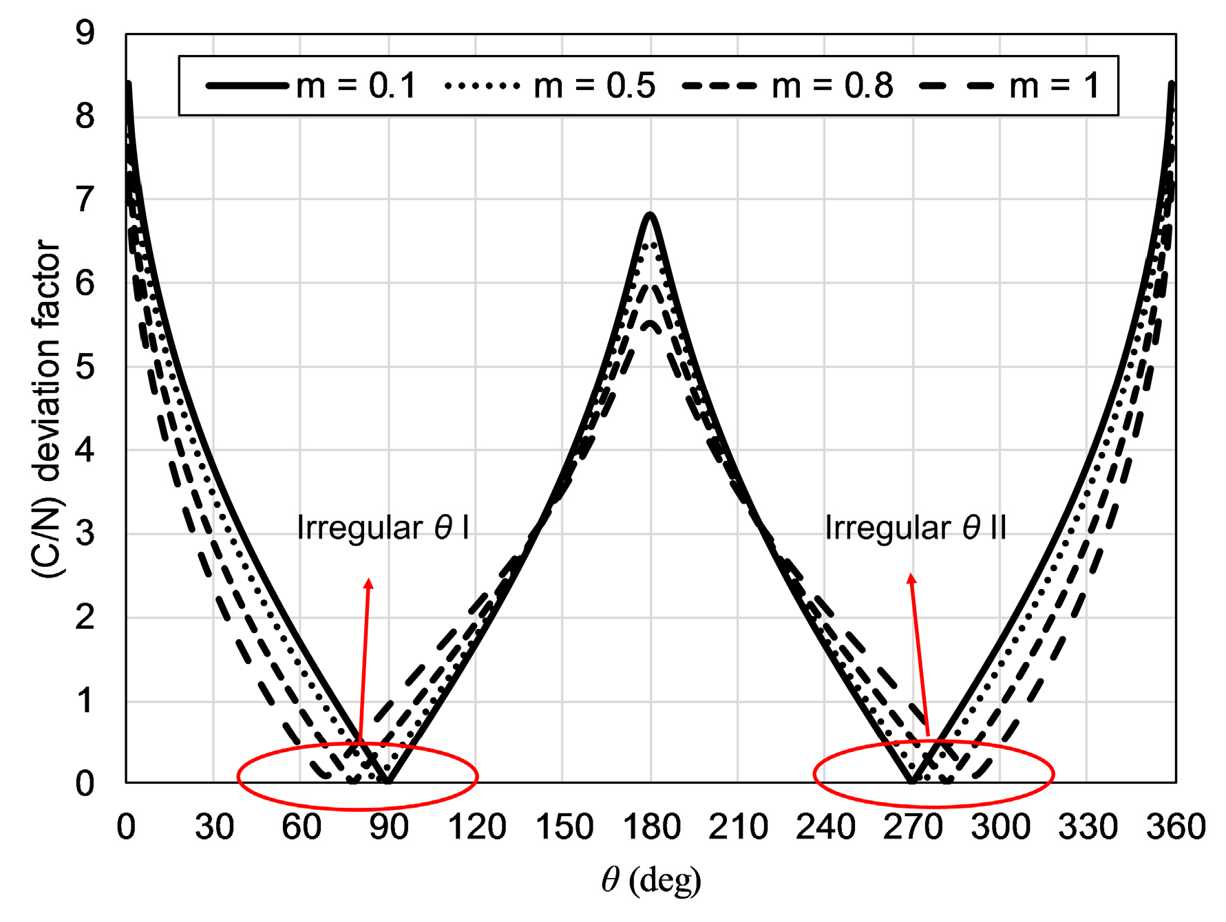
Calculate the (C/N) deviation factor using (27) of all (C/N) penalties in b).
(d)
Repeat steps a) to c) for the value 0° ≤ θ ≤ 360° with step 1°.
(e)
Find θ in step d) which produces the smallest (C/N) deviation factor.
(f)
Repeat steps a) to e) for 0.1 ≤ m ≤ 4 with step 0.1. The value of m is limited to 4 since only in this condition can the sidebands of >10 order be ignored.
The curve for the search of irregular θ is shown in Figure 7. The vertical axis represents the (C/N) deviation factor, and the horizontal one represents the θ value, which varies from 0 to 360°. The θ producing the smallest (C/N) deviation factor is chosen as the irregular θ. For each m, there are two irregular θs. The value of irregular θ I is 90° at m = 0.1, 86° at m = 0.5, 78° at m = 0.8, and 69° at m = 1. Meanwhile, the value of irregular θ II is 270° at m = 0.1, 274° at m = 0.5, 282° at m = 0.8, and 291° at m = 1. The value of irregular θ II = 360° − irregular θ I. The irregular θ for another m is given in Table 1.
To clarify whether the irregular θ is periodical, the researchers investigated it at the range of 360° ≤ θ ≤ 720°, and the results are presented in Figure 8a. For m = 1, the irregular θ I is 429° or 69° + 360°, which means it is periodical. The irregular θ was also investigated at fm = 40 GHz. The results of the calculation, as shown in Figure 8b, conclude that at m = 1, the irregular θ I amounts to 69°. In other words, the irregular θ is the same with the same m despite different fm.
To see the proportion of decrease in (C/N) deviation factor before and after the use of irregular θ, a comparison of (C/N) deviation factor on the RoF link with ODSB, OSSB, and irregular θ modulation was performed. The calculation is performed using λc = 1550 nm (D = 17 ps/(nm km)), and fm = 60 GHz at 0.1 ≤ m ≤ 4. The results of this calculation are shown in Figure 9.
The vertical axis stands for the (C/N) deviation factor, and the horizontal axis represents m. It is visible that the value of the (C/N) deviation factor of RoF link with ODSB modulation is always greater than those of OSSB modulation and irregular θ. The line of (C/N) deviation factor of ODSB at 0.1 < m < 1.6 decreased before fluctuating at m > 1.6. In contrast, the value of (C/N) deviation factor for OSSB and irregular θ increased at 0.1 < m < 1.9 and then fluctuated at m > 1.9. The (C/N) deviation factor for irregular θ is always smaller than OSSB. These findings suggest that the use of irregular θ is able to handle dispersion power fading better than OSSB does on all m. The RoF link with irregular θ has the (C/N) deviation factor < 0.1 at m ≤ 1. This means the irregular θ can cope with dispersion power fading well at m ≤ 1.
To see the performance of irregular θ in handling dispersion power fading, a calculation of the (C/N) penalty at m = 1 for RoF link calculation with irregular θ I = 69°, irregular θ II = 291°, ODSB modulation, and OSSB modulation was performed. The calculation was performed with λc = 1550 nm (D = 17 ps/(nm.km)), and fm = 60 GHz. To validate these results, a comparison of calculation results of (C/N) penalty with the simulation results using Optisystem software was done. The simulation circuit is given in Figure 10.
The structure of the RoF link consists of sine generator, fork 1x2, electrical phase shift, CW laser, MZM, optical fiber, photodetector PIN, band pass rectangle filter, and electrical power meter. The sine generator works to generate pure RF signals. In this simulation, the frequency of sine generator is set to 60 GHz. Because the switching voltage Vπ used in the simulation is 4 V, the voltage of sine generator Vm is set to 1.274 V to obtain m = 1. The output of the sine generator is then duplicated using fork 1x2. The first fork output is inserted into the electrical phase shift and utilized as an MZM top driver, while the second fork output is directly used as an MZM bottom driver. The electrical phase shift is used to differentiate the phase between the first RF signal and the second fork output by θ. The type of MZM used is LiNb-MZM. To produce γ = ½, MZM is set with the parameters as outlined in Table 2. MZM optical inputs are CW laser which is set to λc = 1550 nm, power = 0 dBm, and line width = 10 MHz. The output of MZM is then transmitted through single-mode optical fiber. The optical fiber is configured with parameters in Table 3. In this simulation, the effect of fiber attenuation was ignored. At the receiver, the optical signal is detected using PIN photodetector under the parameter of responsivity (1 A/W) and dark current (10 nA). Because the output of photodetector consists of an electric signal with frequencies of 0, 60, 120 GHz, etc., it was filtered by means of a band pass rectangle filter. To obtain an RF signal at 60 GHz, the parameter filter was used by frequency of 60 GHz, bandwidth of 10 MHz, the insertion loss of 0 dB and a depth of 100 dB. The power of the recovered RF signal was measured using the electrical power meter. The simulation was performed in three scenarios, with the first one being for the RoF link with ODSB modulation scheme. To produce the ODSB modulation scheme, the electrical phase shift is set to θ = 180°. The second scenario is to set θ = 90° to produce OSSB modulation scheme, while the third scenario is for the RoF link with the irregular θ. Since m in this simulation is 1, the electrical phase shift is set to θ = 69 and 291°. The measurements of power for each scenario were performed for 0 to 5 km fiber lengths with a step of 0.1 km.
The (C/N) penalty curve for calculation and simulation results is shown in Figure 11. The curve for the results of both the calculation and simulation from the RoF link with ODSB modulation are the same in pattern. The same pattern of the curve also applied to OSSB modulation and irregular θ (θ = 69° and 291°). This means that the mathematical model used to calculate the recovered RF signal power is correct. On the RoF link with the ODSB modulation scheme, a deep fade occurs at L = 1 and 3.1 km. The deep fade did not occur in the RoF link with OSSB modulation scheme, but there is a reduction in power of about 2.5 dB at the same L. Meanwhile, the power loss on the RoF link with irregular θ = 69° and irregular θ = 291° is extremely small. The (C/N) deviation factor of the RoF link with irregular θ = 69° and irregular θ = 291° is 0.1, with OSSB modulation 0.9, and ODSB modulation 5.5. Therefore, irregular θ could reduce the (C/N) deviation factor by 5.4, while OSSB reduced by 4.6. This suggests the irregular θ handles dispersion power fading better than OSSB does. Irregular θ = 69° and irregular θ = 291° have the same pattern of the curve and performance in handling dispersion power fading.
The calculation of (C/N) penalty was also performed on the RoF link with fm = 30 and 40 GHz at m = 1 to test whether the use of irregular θ can successfully handle the dispersion power fading of RoF link at different fm. The calculation is done with λc = 1550 nm (D = 17 ps/(nm km)). The curve for the results of this calculation is shown in Figure 12.
It is obvious from Figure 12 that the ODSB modulation of RoF link with fm = 30 GHz experienced a deep fade at L = 4.1 km, while that with fm = 40 GHz experienced it at L = 2.3 km. No deep fade was recorded on the RoF link with OSSB modulation, but there remained a power reduction of 2.5 dB at the same L. The reduction on the irregular θ of RoF link was incredibly small. The (C/N) deviation factor with ODSB was 7.8 at fm = 30 GHz and 7.5 at fm = 40 GHz. On the other hand, the (C/N) deviation factor of OSSB was 1.0 at fm = 30 GHz and 0.9 at fm = 40 GHz, while that of irregular θ was 0.1 at fm = 30 GHz and 0.1 at fm = 40 GHz. The figures suggest that the irregular θ handles dispersion power fading better than OSSB in every fm.
To find out whether the irregular θ can overcome dispersion power fading at another λc, the researcher conducted a (C/N) penalty calculation on the RoF link with λc = 1540 nm (D = 16 ps/(nm km)) and λc = 1570 nm (D = 18 ps/(nm km)) at m = 1. Figure 13 portrays the curve for the results of this calculation.
It was found that the RoF link of ODSB modulation with λc = 1570 nm experienced a deep fade at L = 0.9, 2.8 and 4.8 km, while that with λc = 1540 nm experienced the fade at L = 1.1 and 3.3 km. The deep fade did not occur in the RoF link of OSSB or irregular θ, but a substantial power reduction of 2.5 dB occurred with OSSB modulation, whereas the reduction with the irregular θ was exceptionally small. The (C/N) deviation factor of RoF link with ODSB modulation was 8.6, OSSB modulation 0.9, and irregular θ 0.1, all at λc = 1540 nm. The (C/N) deviation factor with λc = 1570 nm for ODSB modulation was 7.3, OSSB modulation 0.9, and irregular θ 0.1. These numbers also imply that the use of irregular θ overcomes dispersion power fading better than OSSB does in any λc.

5. Conclusions

In this paper, the irregular θ method was used to overcome the dispersion power fading on the RoF link using DD-MZM as an E/O converter. The level of dispersion effect on the recovered RF signal power was measured using (C/N) deviation factor. Two irregular θ was set for each m used. Results suggested that the irregular θ overcomes dispersion power fading better than OSSB modulation scheme at all m tested. In addition, the RoF link with irregular θ handled dispersion fading well at m ≤ 1, and it has a fixed (C/N) deviation factor at all fm and λc, which is 0.1 at m = l. All in all, the irregular θ manages to overcome the dispersion power fading at any fm and λc without having to re-adjust the transmitter.

Author Contributions

Conceptualization, F.U.; methodology, F.U. and T.F.; validation, G.W. and P.S.P.; formal analysis, F.U. and T.F; investigation, F.U. and T.F.; data curation, F.U.; writing—original draft preparation, F.U.; writing—review and editing, G.W. and P.S.P.; supervision, G.W. and P.S.P.; project administration, G.W. and P.S.P.; funding acquisition, G.W.

Funding

This research was funded by the Ministry of Research, Technology, and Higher Education of the Republic of Indonesia, under Penelitian Disertasi Doktor (PDD) grant No. NKB-1837/UN2.R3.1/HKP.05.00/2019.

Conflicts of Interest

The authors declare no conflict of interest.

References

  1. Fernando, X.N. Radio over Fiber for Wireless Communications: From Fundamentals to Advanced Topics; John Wiley & Sons: Hoboken, NJ, USA, 2014. [Google Scholar]
  2. Insua, I.G. Optical Generation of mm-Wave Signals for Use in Broadband Radio over Fiber Systems. Ph.D. Thesis, Technische Universität Dresden, Dresden, Germany, 2010. [Google Scholar]
  3. Elwan, H.H.; Poette, J.; Cabon, B. Simplified Chromatic Dispersion Model Applied to Ultra-Wide Optical Spectra for 60 GHz Radio-Over-Fiber Systems. J. Lightwave Technol. 2019, 37, 5115–5121. [Google Scholar] [CrossRef]
  4. Rzaigui, H.; Poette, J.; Cabon, B.; Brendel, F.; Khayatzadeh, R. Optical heterodyning for reduction of chromatic dispersion sensitivity in 60 GHz mode-locked laser systems. J. Lightwave Technol. 2013, 31, 2955–2960. [Google Scholar] [CrossRef]
  5. Brendel, F.; Poette, J.; Cabon, B.; Zwick, T.; van Dijk, F.; Lelarge, F.; Accard, A. Chromatic dispersion in 60 GHz radio-over-fiber networks based on mode-locked lasers. J. Lightwave Technol. 2011, 29, 3810–3816. [Google Scholar] [CrossRef]
  6. Hu, B.-N.; Wang, J.; Wang, W.; Zhao, R.-W. Analysis on Dispersion Compensation with DCF based on Optisystem. In Proceedings of the 2010 2nd International Conference on Industrial and Information Systems, Dalian, China, 10–11 July 2010. [Google Scholar] [CrossRef]
  7. Li, S.; Zheng, X.; Zhang, H.; Zhou, B. Compensation of dispersion-induced power fading for highly linear radio-over-fiber link using carrier phase-shifted double sideband modulation. Opt. Lett. 2011, 36, 546–548. [Google Scholar] [CrossRef] [PubMed]
  8. Liu, J.; Wu, X.; Huang, C.; Tsang, H.K.; Shu, C. Compensation of Dispersion-Induced Power Fading in Analog Photonic Links by Gain-Transparent SBS. IEEE Photonics Technol. Lett. 2018, 30, 688–691. [Google Scholar] [CrossRef]
  9. Gao, Y.; Wen, A.; Liu, L.; Tian, S.; Xiang, S.; Wang, Y. Compensation of the dispersion-induced power fading in an analog photonic link based on PM–IM conversion in a Sagnac loop. J. Lightwave Technol. 2015, 33, 2899–2904. [Google Scholar] [CrossRef]
  10. Chen, Z.; Yan, L.; Jiang, H.; Pan, W.; Luo, B.; Zou, X. Dispersion compensation in analog photonic link utilizing a phase modulator. J. Lightwave Technol. 2014, 32, 4642–4647. [Google Scholar] [CrossRef]
  11. Gao, Y.; Wen, A.; Wu, X.; Wang, Y.; Zhang, H. Efficient photonic microwave mixer with compensation of the chromatic dispersion-induced power fading. J. Lightwave Technol. 2016, 34, 3440–3448. [Google Scholar] [CrossRef]
  12. Yin, C.; Li, J.; Li, B.; Lv, Q.; Dai, J.; Yin, F.; Dai, Y.; Xu, K. Microwave Photonic Frequency Up-Convertor with Frequency Doubling and Compensation of Chromatic-Dispersion-Induced Power Fading. IEEE Photonics J. 2017, 9, 1–7. [Google Scholar] [CrossRef]
  13. Tian, Y.; Lee, K.-L.; Lim, C.; Nirmalathas, A. 60 GHz Analog Radio-Over-Fiber Fronthaul Investigations. J. Lightwave Technol. 2017, 35, 4304–4310. [Google Scholar] [CrossRef]
  14. Dong, Z. 64 QAM vector radio-frequency signal generation based on phase precoding and optical carrier suppression modulation. IEEE Photonics J. 2016, 8, 1–7. [Google Scholar] [CrossRef]
  15. Tian, Y.; Lee, K.-L.; Lim, C.; Nirmalathas, A. Experimental comparison of DSB-SC & OSSB based 60 GHz radio-over-fiber fronthaul links. In Proceedings of the 2016 IEEE International Topical Meeting on Microwave Photonics (MWP), Long Beach, CA, USA, 31 October–3 November 2016. [Google Scholar] [CrossRef]
  16. Ma, J.; Yu, J.; Yu, C.; Xin, X.; Zeng, J.; Chen, L. Fiber dispersion influence on transmission of the optical millimeter-waves generated using LN-MZM intensity modulation. J. Lightwave Technol. 2007, 25, 3244–3256. [Google Scholar] [CrossRef]
  17. Yu, J.; Jia, Z.; Yi, L.; Su, Y.; Chang, G.-K.; Wang, T. Optical millimeter-wave generation or up-conversion using external modulators. IEEE Photonics Technol. Lett. 2006, 18, 265–267. [Google Scholar] [CrossRef]
  18. Wang, K.; Zheng, X.; Zhang, H.; Guo, Y. A radio-over-fiber downstream link employing carrier-suppressed modulation scheme to regenerate and transmit vector signals. IEEE Photonics Technol. Lett. 2007, 19, 1365–1367. [Google Scholar] [CrossRef]
  19. Al-Shareefi, N.A.; Hassan, S.; Malek, F.; Ngah, R.; Aljunid, S.A.; Abbas, S.; Anida, N. A study in OCS millimeter-wave generation using two parallel DD-MZMs. In Proceedings of the 2013 IEEE 11th Malaysia International Conference on Communications (MICC), Kuala Lumpur, Malaysia, 26–28 November 2013. [Google Scholar] [CrossRef]
  20. Lim, C.; Tian, Y.; Lee, K.-L.; Nirmalathas, A. Transport schemes for fiber-based fronthaul for transporting 60 GHz wireless signals. In Proceedings of the 2017 19th International Conference on Transparent Optical Networks (ICTON), Girona, Spain, 2–6 July 2017. [Google Scholar] [CrossRef]
  21. Basha, S.A.H.; Ghosh, D.; Sahu, P. 4-QAM and 16-QAM modulation employing single dual drive Mach-Zehnder modulator and FBG for OFDM-radio-over-fiber system. In Proceedings of the 2017 International Conference on Communication and Signal Processing (ICCSP), Chennai, India, 6–8 April 2017. [Google Scholar] [CrossRef]
  22. Park, M.; Song, J.-I. All-optical frequency upconversion of a quasi optical single sideband signal utilizing a nonlinear semiconductor optical amplifier for radio-over-fiber applications. Opt. Express 2011, 19, 24499–24506. [Google Scholar] [CrossRef] [PubMed]
  23. Paloi, F.; Haxha, S. Analysis of the carrier suppressed single sideband modulation for long distance optical communication systems. Optik 2018, 161, 230–243. [Google Scholar] [CrossRef]
  24. Xie, M.; Zhao, M.; Lei, M.; Wu, Y.; Liu, Y.; Gao, X.; Huang, S. Anti-dispersion phase-tunable microwave mixer based on a dual-drive dual-parallel Mach-Zehnder modulator. Opt. Express 2018, 26, 454–462. [Google Scholar] [CrossRef]
  25. Krishna, V.R.; Singhal, R. Dual carrier multiplexed M-QAM signals modulated optical SSB transmission over fiber. In Proceedings of the 2016 Thirteenth International Conference on Wireless and Optical Communications Networks (WOCN), Hyderabad, India, 21–23 July 2016. [Google Scholar] [CrossRef]
  26. Ma, J. Dual-tone QPSK optical millimeter-wave signal generation by frequency nonupling the RF signal without phase precoding. IEEE Photonics J. 2016, 8, 1–7. [Google Scholar] [CrossRef]
  27. Chen, X.; Yao, J. A High Spectral Efficiency Coherent RoF System Based on OSSB Modulation with Low-Cost Free-Running Laser Sources for UDWDM-PONs. J. Lightwave Technol. 2016, 34, 2789–2795. [Google Scholar] [CrossRef]
  28. Lim, C.; Nirmalathas, A.; Lee, K.-L.; Novak, D.; Waterhouse, R. Intermodulation distortion improvement for fiber–radio applications incorporating OSSB+ C modulation in an optical integrated-access environment. J. Lightwave Technol. 2007, 25, 1602–1612. [Google Scholar] [CrossRef]
  29. Peng, Z.; Wen, A.; Gao, Y.; Tu, Z.; Chen, W.; Zhang, W. A novel method to realize optical single sideband modulation with tunable optical carrier to sideband ratio. Microw. Opt. Technol. Lett. 2017, 59, 1740–1743. [Google Scholar] [CrossRef]
  30. Zheng, Z.; Peng, M.; Zhou, H.; Chen, M.; Jiang, L.; Tan, L.; Dai, X.; Xiang, Y. Optical single sideband millimeter-wave signal generation and transmission using 120° hybrid coupler. Opt. Commun. 2018, 411, 21–26. [Google Scholar] [CrossRef]
  31. Shen, Y.; Zhang, X.; Chen, K. Optical single sideband modulation of 11-GHz RoF system using stimulated Brillouin scattering. IEEE Photonics Technol. Lett. 2005, 17, 1277–1279. [Google Scholar] [CrossRef]
  32. Sung, H.-K.; Lau, E.K.; Wu, M.C. Optical single sideband modulation using strong optical injection-locked semiconductor lasers. IEEE Photonics Technol. Lett. 2007, 19, 1005–1007. [Google Scholar] [CrossRef]
  33. Wu, B.; Wang, M.; Tang, Y.; Sun, J.; Zhang, J.; Yan, F.; Jian, S. Optical single sideband modulation with tunable optical carrier-to-sideband ratio using a modulator in a Sagnac loop. Opt. Laser Technol. 2017, 91, 98–102. [Google Scholar] [CrossRef]
  34. Thomas, V.A.; El-Hajjar, M.; Hanzo, L. Optical single sideband signal generation relying on a single-drive Mach–Zehnder modulator for radio over fibre communications. IET Commun. 2016, 10, 534–539. [Google Scholar] [CrossRef]
  35. Lee, U.-S.; Jung, H.-D.; Han, S.-K. Optical single sideband signal generation using phase modulation of semiconductor optical amplifier. IEEE Photonics Technol. Lett. 2004, 16, 1373–1375. [Google Scholar] [CrossRef]
  36. Li, Z.; Chi, H.; Zhang, X.; Yao, J. Optical single-sideband modulation using a fiber-Bragg-grating-based optical Hilbert transformer. IEEE Photonics Technol. Lett. 2011, 23, 558–560. [Google Scholar] [CrossRef]
  37. Xue, M.; Pan, S.; Zhao, Y. Optical spectral response measurement based on optical single-sideband modulation with doubled measurement range. Electron. Lett. 2016, 52, 852–853. [Google Scholar] [CrossRef]
  38. Chang, C.-H.; Chang, J.-H. Optical SSB modulation scheme based on phase-modulator and vertical-cavity-surface-emitting laser. In Proceedings of the 2014 Conference on Lasers and Electro-Optics (CLEO)—Laser Science to Photonic Applications, San Jose, CA, USA, 8–13 June 2014. [Google Scholar] [CrossRef]
  39. Parajuli, H.N.; Udvary, E. Optimization of optical carrier to sideband ratio for the concatenated AM-PM based optical single sideband radio over fiber system. In Proceedings of the 2016 21st European Conference on Networks and Optical Communications (NOC), Lisbon, Portugal, 1–3 June 2016. [Google Scholar] [CrossRef]
  40. Smith, G.H.; Novak, D.; Ahmed, Z. Overcoming chromatic-dispersion effects in fiber-wireless systems incorporating external modulators. IEEE Trans. Microw. Theory Tech. 1997, 45, 1410–1415. [Google Scholar] [CrossRef]
  41. Patel, D.; Singh, V.K.; Dalal, U. Performance analysis of optical double sideband and optical single sideband generation using mach zehnder modulator chirp and extinction ratio over different fiber link. In Proceedings of the 2017 2nd International Conference for Convergence in Technology (I2CT), Mumbai, India, 7–9 April 2017. [Google Scholar] [CrossRef]
  42. Shimotsu, S.; Oikawa, S.; Saitou, T.; Mitsugi, N.; Kubodera, K.; Kawanishi, T.; Izutsu, M. Single side-band modulation performance of a LiNbO 3 integrated modulator consisting of four-phase modulator waveguides. IEEE Photonics Technol. Lett. 2001, 13, 364–366. [Google Scholar] [CrossRef]
  43. Hervé, D.; Corral, J.L.; Fuster, J.M.; Herrera, J.; Martinez, A.; Polo, V.; Ramos, F.; Vourc’h, E.; Marti, J. Techniques for the compensation for chromatic-dispersion effects in fiber-wireless systems. Ursi Radio Sci. Bull. 2004, 2004, 26–37. [Google Scholar] [CrossRef]
  44. Xue, M.; Pan, S.; Zhao, Y. Optical single-sideband modulation based on a dual-drive MZM and a 120 hybrid coupler. J. Lightwave Technol. 2014, 32, 3317–3323. [Google Scholar] [CrossRef]
  45. Ujang, F.; Wibisono, G. A Single DD-MZM for Generating Vestigial Sideband Modulation Scheme in Radio over Fiber Systems. In Proceedings of the 2018 2nd International Conference on Electrical Engineering and Informatics (ICon EEI), Batam, Indonesi, 16–17 October 2018. [Google Scholar] [CrossRef]
  46. Colton, D.; Kress, R. Inverse Acoustic and Electromagnetic Scattering Theory, 3rd ed.; Springer Science & Business Media: Heidelberg, Germany, 1998; p. 32. [Google Scholar]
  47. Davies, R.J. Optical Single Sideband for Broadband and Subcarrier Systems; University of Alberta: Edmonton, AB, Canada, 1999. [Google Scholar]
  48. Meslener, G. Chromatic dispersion induced distortion of modulated monochromatic light employing direct detection. IEEE J. Quantum Electron. 1984, 20, 1208–1216. [Google Scholar] [CrossRef]
Figure 1. Schematic diagram of dual-drive Mach–Zehnder modulator (DD-MZM).
Photonics 06 00104 g001
Figure 2. The spectrum of a modulated optical signal. (a) DD-MZM as an optical double-sideband (ODSB) modulator and (b) OSSB modulator.
Photonics 06 00104 g002
Figure 3. Radio-over-fiber (RoF) link with DD-MZM as electro-optic (E/O) converter.
Photonics 06 00104 g003
Figure 4. Carrier-to-noise (C/N) penalty on the RoF link with ODSB modulation (a) m ≤ 1 (b) m > 1.
Photonics 06 00104 g004
Figure 5. The (C/N) penalty on the RoF link with ODSB modulation (a) variation fm, (b) variation λc.
Photonics 06 00104 g005
Figure 6. (C/N) penalty on the RoF link with OSSB modulation, (a) m ≤ 1, (b) m > 1, (c) variation fm and (d) variation λc.
Photonics 06 00104 g006aPhotonics 06 00104 g006b
Figure 7. (C/N) deviation factor as a function of θ.
Photonics 06 00104 g007
Figure 8. (C/N) deviation factor (a) 360° ≤ θ ≤ 720° (b) at fm = 40 GHz.
Photonics 06 00104 g008
Figure 9. The (C/N) deviation factor of RoF link with ODSB, OSSB modulation schemes, and irregular θ.
Photonics 06 00104 g009
Figure 10. The structure of RoF link simulation using Optisystem software.
Photonics 06 00104 g010
Figure 11. (C/N) penalty of RoF link with ODSB, OSSB modulation, and irregular θ: The results of calculation and simulation.
Photonics 06 00104 g011
Figure 12. (C/N) penalty of RoF link with ODSB, OSSB modulation, and irregular θ for fm = 30 and 40 GHz.
Photonics 06 00104 g012
Figure 13. The (C/N) penalty for RoF link with ODSB, OSSB, and irregular θ modulation at λc = 1540 nm and 1570 nm.
Photonics 06 00104 g013
Table 1. Irregular θ for m = 0.1–4.
mIrregular θ I (Degrees)Irregular θ II
(Degrees)
mIrregular θ I
(Degrees)
Irregular θ II (Degrees)
0.1902702.188272
0.2892712.285275
0.3892712.379281
0.4882722.473287
0.5862742.568292
0.6842762.665295
0.7812792.762298
0.8782822.860300
0.9742862.959301
1.0692913.058302
1.1632973.118342
1.2563043.215345
1.3503103.3105255
1.4443163.4107256
1.5383223.5108252
1.6323283.6107253
1.7283323.7105255
1.81452153.8103257
1.91422183.947313
2.0862744.045315
Table 2. Setting parameter of LiNb-MZM.
ParameterValueUnits
Extinction ratio20dB
Switching bias voltage4V
Switching radio frequency (RF) voltage4V
Insertion loss0dB
Normalize electrical signalunchecked-
Bias voltage10V
Bias voltage22V
Table 3. Setting parameter of optical fiber.
ParameterValueUnits
User-defined reference wavelengthChecked-
Reference wavelength1550nm
Length0–5km
Attenuation effectUnchecked-
Group velocity dispersionChecked-
Third-order dispersionUnchecked-
Frequency domain parameterUnchecked-
Dispersion17ps/nm/km

