Article

Excitation Schemes of Plasmonic Angular Ring Resonator-Based Band-Pass Filters Using a MIM Waveguide

by
Vishwanath Mittapalli
1,2,* and
Habibulla Khan
1
1
Department of Electronics and Communication Engineering, Koneru Lakshmaiah Education Foundation, Guntur 522502, Andhra Pradesh, India
2
Department of Electronics and Communication Engineering, Marri Laxman Reddy Institute of Technology and Management, Hyderabad 500043, Telangana, India
*
Author to whom correspondence should be addressed.
Photonics 2019, 6(2), 41; https://doi.org/10.3390/photonics6020041
Submission received: 19 March 2019 / Revised: 2 April 2019 / Accepted: 9 April 2019 / Published: 11 April 2019

Abstract

:
This article describes the analysis and design of the excitation schemes of the plasmonic angular ring resonator-based band-pass filters using a metal-insulator-metal (MIM) waveguide. The excitation schemes of the plasmonic angular ring resonator-based band-pass filters have been analyzed in terms of their physical length by using commercially available electromagnetic full-wave simulation software (CST microwave studio). The excitation schemes of the plasmonic angular ring resonator-based band-pass filter using a MIM waveguide have been realized at the optical O (1260–1360 nm) and U (1625–1675 nm) bands, respectively, as it has dual-band characteristics. The excitation schemes of the plasmonic angular ring resonators have been designed and simulated to determine the variation in transmission and reflection coefficients. The magnetic field distribution of the proposed filters was observed. The ring resonators require low power and had a compact size, which was further used for the development of photonic integrated circuits (PICs). The applications of these resonators are further extended and they are used in the development of antennas, branch line couplers, directional couplers and diplexers.

1. Introduction

For the past few decades, copper has been used as a medium for on-chip or off-chip integrated circuits. Below 100 nm, the copper interconnects have been shown to suffer from issues, such as wave reflection, unit area, cross-talk, clock distortion, attenuation and interconnection density limitations. Though Moore’s law predicts that the transistor density will double every 18 months, the same trend is not applicable to copper interconnects. This limitation arises due to the fact that the power dissipation per unit area is able to raise the temperature of the silicon chip substrate up to the silicon’s melting point due to the reduced circuit size [1,2]. The optical waveguides provide an appropriate alternative as it is considered to be a low power dissipating medium. These waveguides mostly operate in TE (transverse-electric) or TM (transverse-magnetic) modes, where each mode has several cut-off conditions depending on the physical size of the waveguide. Due to these cut-off conditions, the waveguide dimensions cannot be reduced beyond a certain limit. Therefore, a limitation arises that is related to the required scaling of the interconnections, due to the increased density of transistors. Onbasli et al. [3] have shown that the waveguides for the near-infrared region (780–3000 nm) need to have dimensions that are larger than ~400 nm. A further reduction in the size of optical waveguide dimensions is possible only if one can find a mode (other than higher order waveguide modes) that can exist and propagate even when the waveguide is operating below the cut-off conditions of the dominant fundamental mode. Plasmonic waveguides are attractive as they support an electromagnetic mode, which can carry a signal through the waveguide, even when operating below the cut-off conditions of the dominant mode [4,5].
The plasma model, in which a gas composed of free electrons moves against a bound positive ion core, has been used to explain the optical properties of metals. The dielectric function of the free electron gas can be written as:
ε ( ω ) = ε 1 + j ε 2 = 1 ω p 2 ω 2 + j γ ω
where:
ε 1 ( ω ) = 1 ω p 2 τ 2 1 + ω 2 τ 2
ε 2 ( ω ) = ω p 2 τ 2 ω ( 1 + ω 2 τ 2 )
γ = 1 τ
where γ represents the collision frequency; τ represents the relaxation time; and ωp represents the plasma frequency.
Surface plasmon polaritons (SPPs) are a type of EM wave that propagates along the metal–dielectric interface. A prominent ability of SPPs is the surpassing of the diffraction limit of the optical wave on the nanoscale [6]. Due to this feature, SPPs are used in highly integrated optical circuits as information carriers. Recently, several optical devices, such as antennas [7], nanowires [8], disc resonators [9], tapered grooves [10], bends, splitters [11] and filters [12], have been investigated experimentally or theoretically. In recent years, SPPs has shown potential in many different applications, such as manipulating and guiding the light on deep subwavelength scales [13,14]. Among these configurations, metal-insulator-metal (MIM) is the most promising technique for the design of nanoscale photonic integrated circuits. MIM waveguide-based devices, such as ultra-wideband resonators, antennas, band reject filters and bandpass filters, have been proposed and were subsequently experimentally or theoretically investigated. MIM waveguide structures have an acceptable propagation length and allow for the strong confinement of light. Consequently, several filters are available and they are very important for transmitting the light in nanophotonics, as they can allow light only at given wavelengths, with the light not allowed to pass on other wavelengths. As a result, there is the need to find an SPP filter with a simple design that can have concurrent dual-band operation in between O and U bands.
Planar plasmonic waveguides are classified into two categories, which are namely the MIM (metal-insulator-metal) and IMI (insulator-metal-insulator) waveguides [15,16]. Generally, the resonators behave as filters, which can accept or reject specific wavelengths from an input signal in a single or dual-band. The transmission line resonators have low Q-values compared to waveguide-based resonators, but they have a simple design, are smaller in size and have large applicability to different nanophotonic circuits [17]. The MIM waveguide-based resonators in cylindrical and rectangular shapes can be used at THz frequencies in the design of filters and other tuning elements.
In the past, Gopalakrishna et al. [18] proposed the excitation schemes of angular ring resonator at the microwave frequency ranges in order to observe the lowest insertion loss devices. The excitation schemes at microwave frequency ranges have been designed at a fundamental frequency of 2.5 GHz. In order to reduce the size and increase the efficiency of the ring resonator, we had proposed the excitation schemes (A), (B) and (C) at the optical wavelengths. There are four excitation schemes of the ring resonator among them. We recently proposed the first excitation scheme in Reference [19] and remaining excitation schemes are proposed in this article. Depending on the feeding techniques, the resonators are classified into the excitation schemes of the angular resonator. The excitation schemes (A), (B) and (C) are the most promising techniques and can be further realized in the coplanar waveguides.
Recently, Rahman et al. [20] proposed the concept of ultra-wide-band band-pass filters, based on the ring resonator, using a plasmonic MIM waveguide. These concentrate on the angular ring resonator, an open loop ring resonator, a u-shaped open loop ring resonator and a square ring resonator with an ultra-wide-band response at optical wavelengths. The response of the ultra-wide-band filters has been observed to be in between the optical O-band to optical L-band (1260–1625 nm).
The ultra-wide response-based bandpass filters allow the passage of unwanted wavelengths, which results in the high noise systems. Although the ultra-wide-band band-pass filter has adopted a curvature feeding technique, we eliminated curvature feeding in order to observe the concurrent dual-band response. In order to avoid the unwanted frequency response, we developed new feeding techniques, which help in the generation of a concurrent dual-band response. The concurrent dual-band filter is a narrow band filter, which allows only certain wavelengths to experience a low insertion loss at two wavelengths concurrently. The past two devices need to be cascaded in order to observe the dual-band response, but in this article, we propose a concurrent dual-band response in a single device, in order to eliminate the other device. This helps in low power consumption and low-cost devices. The proposed excitation scheme allows for a concurrent dual-band response (i.e., it only allows particular frequency ranges and rejects all other unwanted frequency ranges). In order to overcome the drawbacks of ultra-wide-band filters, we propose excitation schemes of the angular plasmonic ring resonator.
The excitation schemes of the angular plasmonic ring resonator were realized at the optical wavelengths of the O (1260–1360 nm) and U (1625–1675 nm) bands. The excitation schemes of the angular ring resonators were realized through FDTM (Finite-difference time-domain) using commercially available software (CST microwave studio suite). Usually, the MIM waveguide-based plasmonic ring resonator has two feed lines and a cylindrical structure that is sandwiched between the two feed lines (0° and 180°). The excitation schemes of the plasmonic angular ring resonator provided a different type of response when the feeding of the resonator was varied. By comparing the various feeding techniques, we could determine which excitation scheme had a high gain, fewer losses and a compact size. The excitation modes of the angular plasmonic ring resonator were designed with metal layers of silver. In these modes, we assigned the following values to the variables: ε = 3.7, and γ = 2.73 × 10¹³ rad/sec [21]. Furthermore, the dielectric was assumed to be silica with a dielectric constant (εi) of 2.50.
In this article, we designed three excitation schemes (A), (B) and (C), which adopted different coupling peripheries in order to develop a high gain device with low insertion loss. By comparing all the three excitation schemes physically, we determined that there were different coupling peripheries. Section 2 of this article describes the excitation scheme of the angular resonator (A) with a low coupling periphery compared to the remaining structures. Section 3 of this article describes the excitation scheme of the angular resonator (B) with a high coupling periphery compared to the angular resonator (A). Section 4 of this article describes the excitation scheme (C) by chamfering the feed lines of the angular resonator.

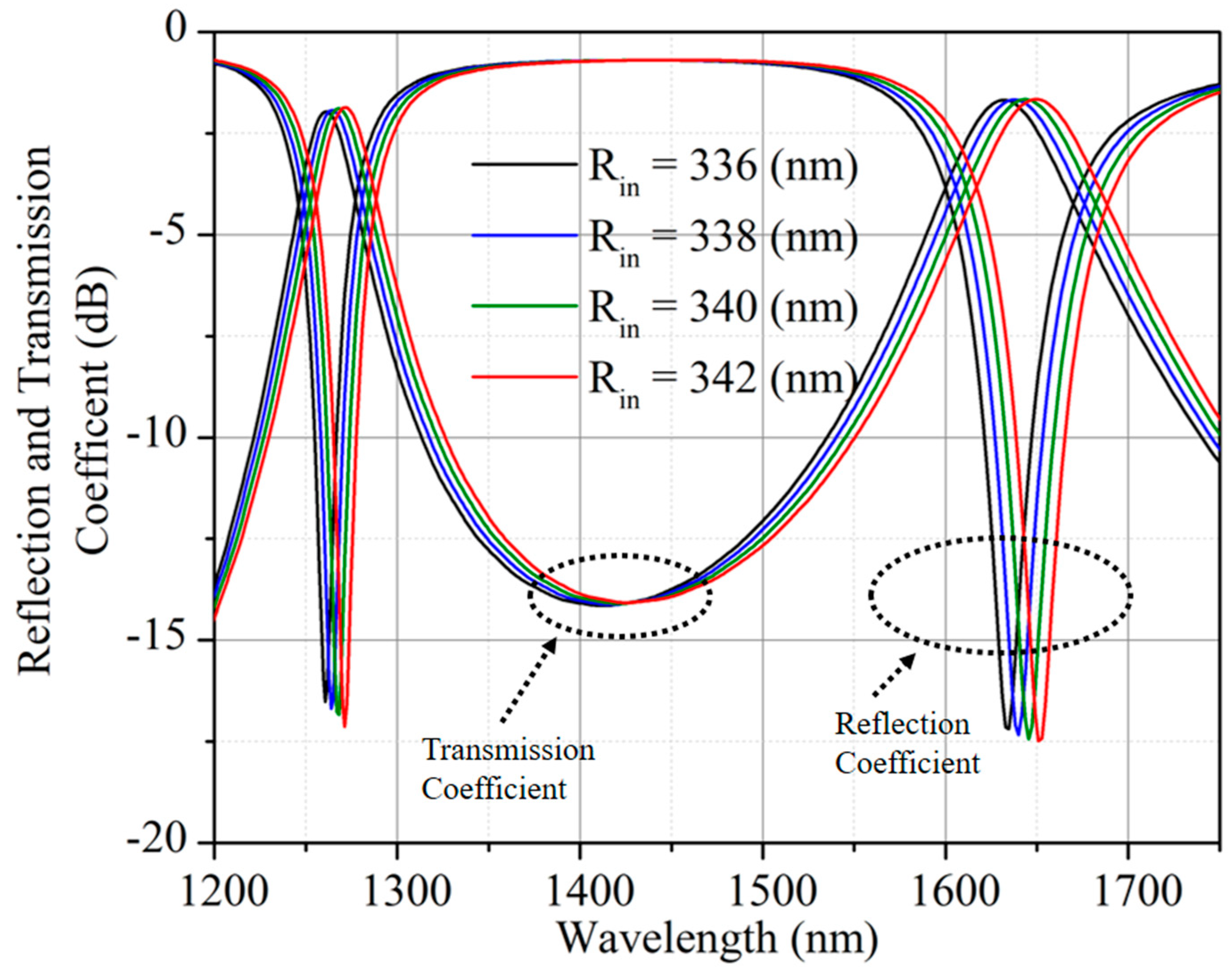
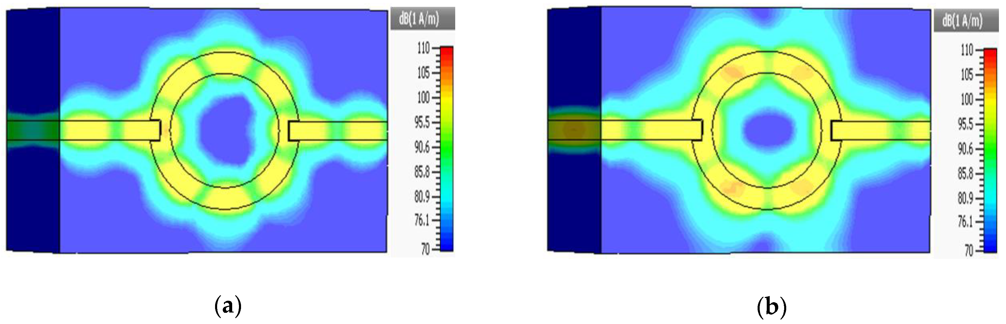
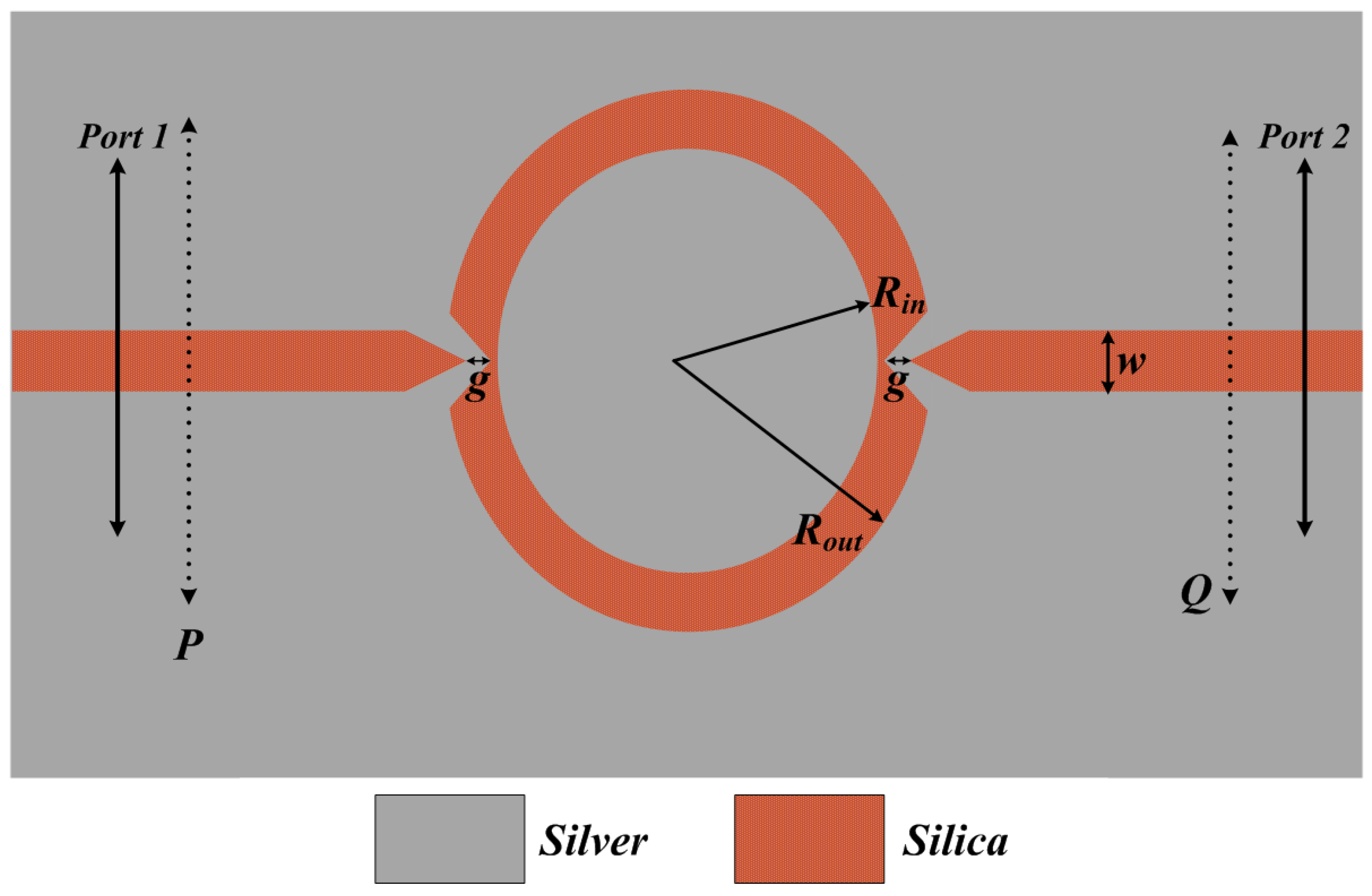
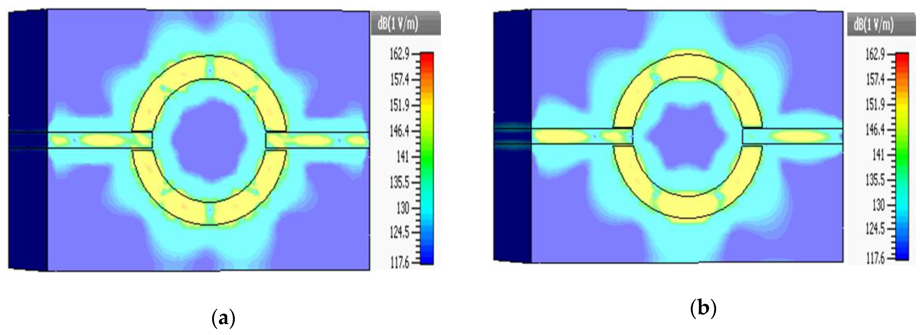
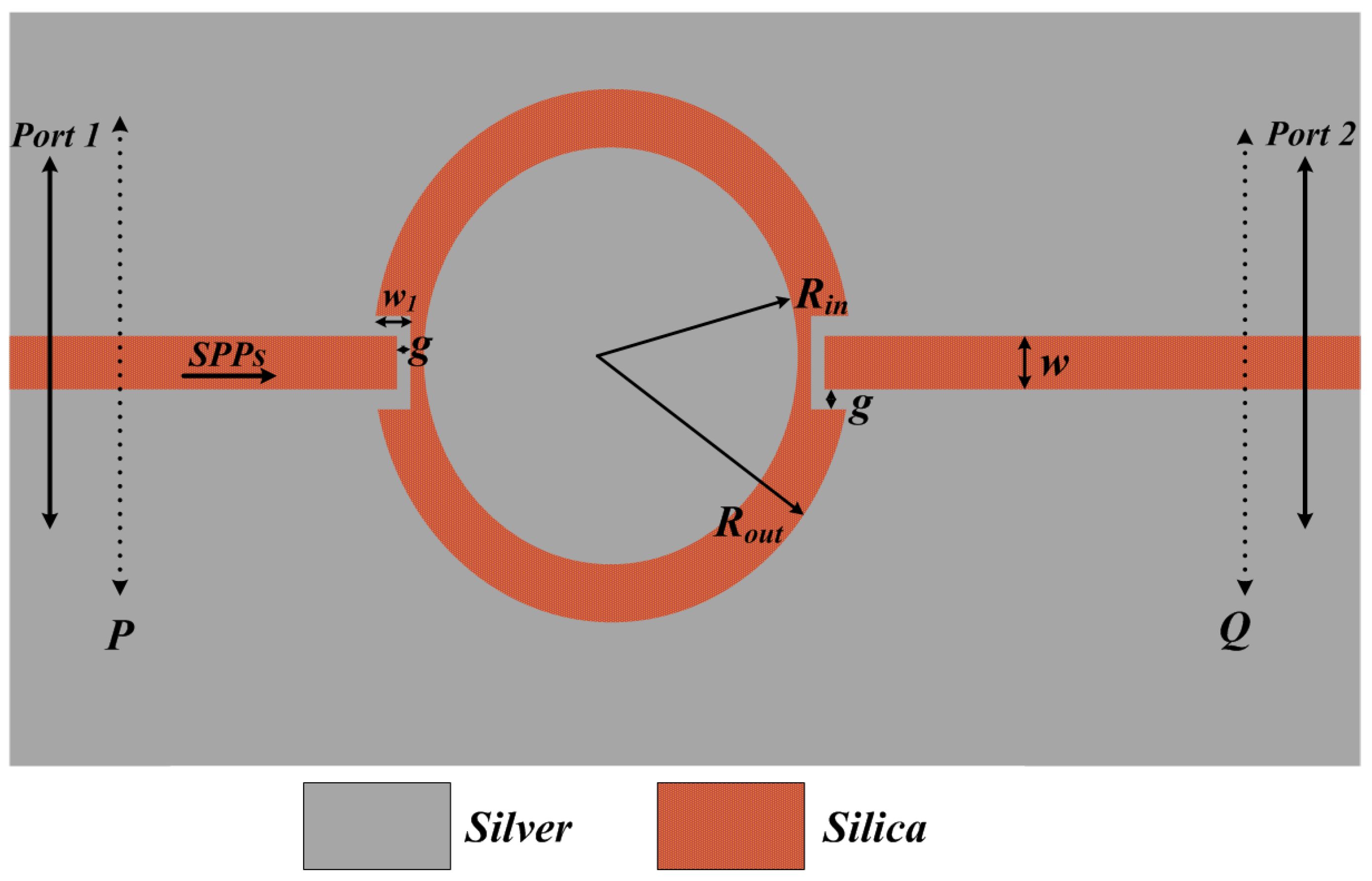
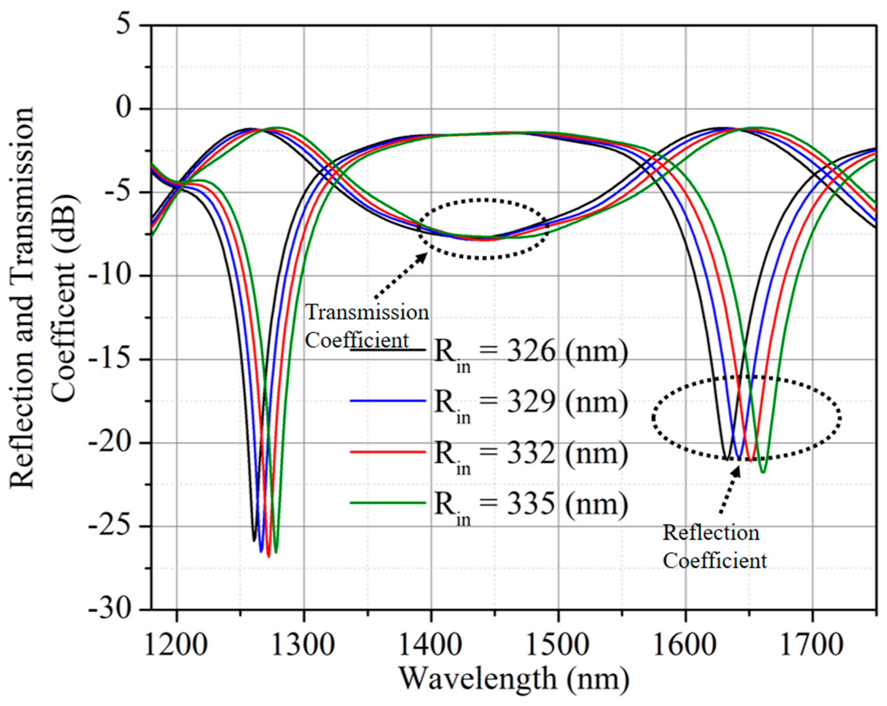
2. Geometry and Operation of Angular Ring Resonator (A) Using MIM Waveguide

The geometry of the plasmonic angular ring resonator (A) using a MIM waveguide is shown in Figure 1. The MIM waveguide-based angular ring resonator usually consists of two feed lines, two semi-infinite metallic layers and an angular ring at the center between the two feed lines. The outer radius is denoted by Rout and the inner radius by Rin, in which the actual radius of the ring is considered to be the mean value of Rout and Rin (i.e., Rm = (Rout + Rin)/2). The length of the feed line is infinite and is separated from the gap g of the angular ring with the inner radius Rin. The width of the feed line is represented as w.
The dimensions of the plasmonic dual-band angular ring resonator bandpass filter (A) using a MIM waveguide were chosen to be Rin = 340 nm, Rout = 465 nm, w = 88 nm and g = 9 nm. The plasmonic angular ring resonator was operated at the optical O and U bands simultaneously with a gain of −17 dB. Figure 2 represents the field distribution of the plasmonic angular ring resonator (A) at optical wavelengths at the O (λ = 1268 nm) and U (λ = 1645 nm) bands. The variation in the reflection and transmission characteristics, with respect to inner radius Rin, is shown in Figure 3.

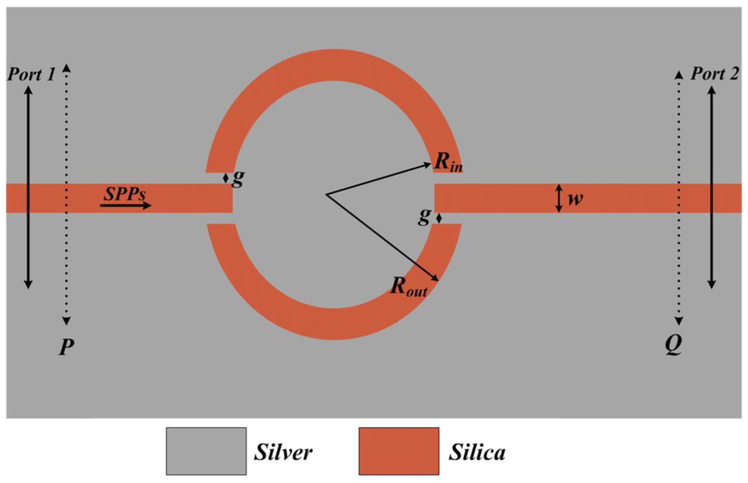
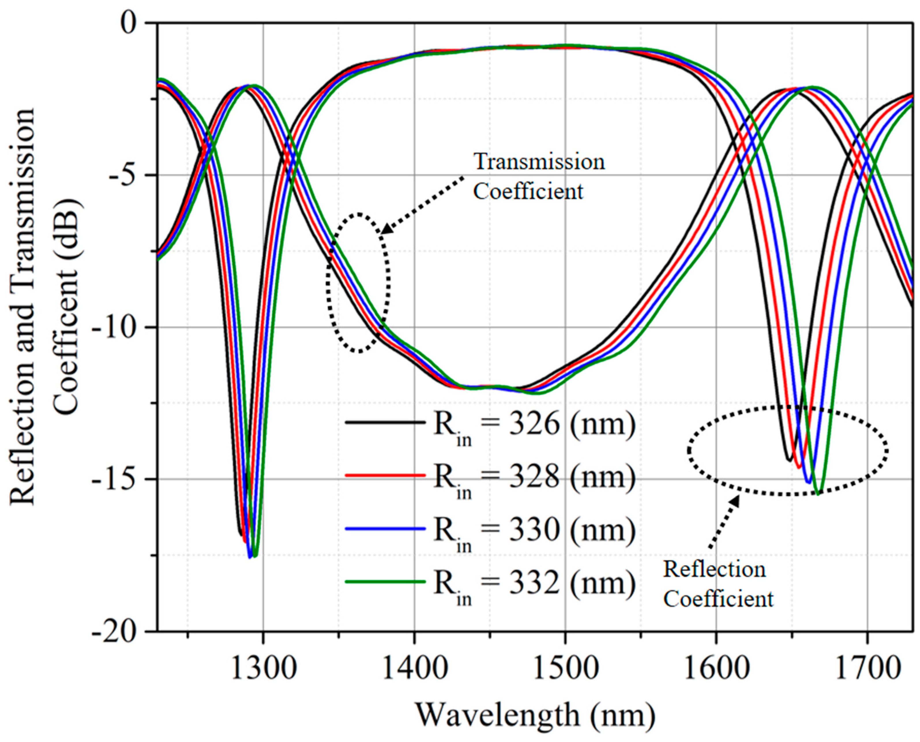
3. Geometry and Operation of Angular Ring Resonator (B) Using MIM Waveguide

The geometry of the plasmonic angular ring resonator (B) using a MIM waveguide is shown in Figure 4. Compared to the angular ring resonator (A), the plasmonic angular ring resonator was proposed in order to increase the coupling periphery by employing a different scheme (B). In this scheme, Rin and Rout were the inner radius and outer radius of the proposed angular ring resonator bandpass filter scheme (B). The length of the feed line was infinite and separated from the gap g, which penetrated the angular ring at a width w1 from the angular ring outer radius Rout.
The dimensions of the plasmonic dual-band angular ring resonator bandpass filter (B) using a MIM waveguide were chosen to be Rin = 332 nm, Rout = 456 nm, w = 108 nm, g = 6 nm and w1 = 66 nm. The plasmonic angular ring resonator (B) was also operated at the optical O (λ = 1272 nm) and U (λ = 1650 nm) bands simultaneously with a minimum gain of −23 dB. The variation in the reflection and transmission characteristics, with respect to the inner radius Rin, is shown in Figure 5. When the inner radius of the angular ring increased, the return loss shifted from left to right in the optical wavelengths. Figure 6 represents the field distribution of the plasmonic angular ring resonator (B) at optical wavelengths of the O (λ = 1272 nm) and U (λ = 1650 nm) bands.

4. Geometry and Operation of Angular Ring Resonator (C) Using MIM Waveguide

The geometry of the plasmonic angular ring resonator (C) using a MIM waveguide is shown in Figure 7. Being different to the angular ring resonator (B), a plasmonic angular ring resonator (C) was proposed with tapered feed lines, which were fed into V-shaped grooves that were etched into the plasmonic angular ring resonator. Similar to the ring resonator (B), the feed line length of the plasmonic angular ring resonator (C) was also chosen to be infinite. The gap between the V-shape groove and the tapered feed line was chosen to be g with a feed line width of w. The inner and outer radius of the angular ring was chosen to be Rin and Rout, respectively.
The dimensions of the plasmonic dual-band angular ring resonator bandpass filter (C) using a MIM waveguide were chosen to be Rin = 332 nm, Rout = 457 nm, w = 120 nm and g = 7 nm. The plasmonic angular ring resonator (C) was operated at the optical O (λ = 1294 nm) and U (λ = 1667 nm) bands simultaneously, with a minimum gain of −15 dB. The variation in the reflection and transmission characteristics, with respect to the inner radius Rin, is shown in Figure 8. When the inner radius of the angular ring increased, the return loss shifted from left to right in the optical wavelengths. Figure 9 represents the field distribution of the plasmonic angular ring resonator (B) at optical wavelengths of O (λ = 1294 nm) and U (λ = 1667 nm) bands.

5. Conclusions

The three excitation schemes of an angular plasmonic band-pass filter using a ring resonator have been analyzed at the O (1260–1360 nm) and U (1625–1675 nm) optical wavelengths, respectively. The plasmonic angular ring resonator band-pass filter was simultaneously operated at two optical wavelengths. The angular ring resonator (A) was analyzed at O (λ = 1268 nm) and U (λ = 1645 nm) with a gain of −17 dB. Similarly, the angular ring resonator (B) was analyzed at O (λ = 1272 nm) and U (λ = 1650 nm) wavelengths with a minimum gain of −23 dB. Finally, the angular ring resonator (C) was analyzed at the O (λ = 1294 nm) and U (λ = 1667 nm) wavelengths with a minimum gain of −15 dB. The transmission performance of the angular plasmonic ring resonator was consistent with the theoretical calculations or numerical calculations. The angular ring resonator (B) had a higher gain and fewer loses compared to the angular rings (A) and (C). This article provides a promising application for the plasmonic dual-band band-pass filter and plasmonic integrated circuits. This structure can also be extended to the design of several other components, such as couplers, diplexers and power splitters/combiners.

Author Contributions

Conceptualization, V.M.; Methodology, V.M. and H.K.; Software, V.M.; Validation, V.M. and H.K.; Formal Analysis, V.M.; Investigation, V.M.; Resources, V.M. and H.K.; Writing-Review & Editing, V.M. and H.K.; Visualization, V.M.; Supervision, H.K.

Funding

The authors acknowledge support by the Koneru Lakshmaiah Education Foundation, Guntur, Andhra Pradesh, India.

Conflicts of Interest

The authors declare no conflict of interest.

References

  1. Tang, L.; Latif, S.; Miller, D.B. Plasmonic device in Si CMOS. In Proceedings of the LEOS 2008 21st Annual Meeting of the IEEE Lasers and Electro-Optics Society, Acapulco, Mexico, 9–13 November 2008; pp. 139–140. [Google Scholar]
  2. Duan, H.; Dominguez, A.I.F.; Bosman, M.; Maier, S.A.; Yang, J.K.W. Nanoplasmonics: Classical down to the Nanometer Scale. Nano Lett. 2012, 12, 1683–1689. [Google Scholar] [CrossRef] [PubMed]
  3. Onbasli, M.C.; Okyay, A.K. Nanoantenna Couplers for Metal-Insulator-Metal Waveguide Interconnects. In Proceedings of the SPIE, San Diego, CA, USA, 10 September 2010; Volume 7757, p. 77573R-1-11. [Google Scholar]
  4. Barnes, W.L.; Dereux, A.; Ebbesen, T.W. Surface plasmon subwavelength optics. Nature 2003, 424, 824–830. [Google Scholar] [CrossRef] [PubMed]
  5. Conway, J.A.; Sahni, S.; Szkopek, T. Plasmonic interconnects versus conventional interconnects: A comparison of latency, crosstalk and energy costs. Opt. Express 2007, 15, 4474–4484. [Google Scholar] [CrossRef] [PubMed]
  6. Zhu, J.H.; Wang, Q.J.; Shum, P.; Huang, X.G. A Simple Nanometeric Plasmonic Narrow-Band Filter Structure Based on Metal-Insulator-Metal Waveguide. IEEE Trans. Nanotechnol. 2011, 10, 1371–1376. [Google Scholar] [CrossRef]
  7. Chityala, R.K. Nanoplasmonic concurrent dual-band antennas using metal-insulator-metal step impedance resonators. Microw. Opt. Technol. Lett. 2019. [Google Scholar] [CrossRef]
  8. Masashi, M.; Akira, K.; Yusuke, N.; Junichi, T. Electromechanically Tunable Plasmonic Nanowires Operating in Visible Wavelengths. ACS Photonics 2016, 3, 2268–2274. [Google Scholar]
  9. Randhawa, S.; Krasavin, A.V.; Holmgaard, T.; Renger, J.; Bozhevolnyi, S.I.; Zayats, A.V.; Quidant, R. Experimental demonstration of dielectric-loaded plasmonic waveguide disk resonators at telecom wavelengths Experimental demonstration of dielectric-loaded plasmonic waveguide disk resonators at telecom wavelengths. Appl. Phys. Lett. 2011, 98, 161102. [Google Scholar] [CrossRef]
  10. Smith, C.L.C.; Stenger, N.; Kristensen, A.; Mortensen, N.A. Gap and channeled plasmons in tapered grooves: A review. R. Soc. Chem. 2015, 7, 79–82. [Google Scholar] [CrossRef] [PubMed]
  11. Veronis, G.; Fan, S.; Veronis, G.; Fan, S. Bends and splitters in metal-dielectric-metal subwavelength plasmonic waveguides Bends and splitters in metal-dielectric-metal subwavelength plasmonic waveguides. Appl. Phys. Lett. 2005, 87, 131102. [Google Scholar] [CrossRef]
  12. Liu, D.; Wang, J.; Zhang, F.; Pan, Y.; Lu, J.; Ni, X. Tunable Plasmonic Band-Pass Filter with Dual Side-Coupled Circular Ring Resonators. Sensors 2017, 17, 585. [Google Scholar] [CrossRef] [PubMed]
  13. Lezec, H.J.; Degiron, A.; Devaux, E.; Linke, R.A.; Martin-Moreno, L.; Garcia-Vidal, F.J.; Ebbesen, T.W. Beaming light from a subwavelength aperture. Science 2002, 297, 820–822. [Google Scholar] [CrossRef] [PubMed]
  14. Pile, D.F.P.; Gramotnev, D.K. Plasmonic subwavelength waveguides: Next to zero losses at sharp bends. Opt. Lett. 2005, 30, 1186–1188. [Google Scholar] [CrossRef] [PubMed]
  15. Taylor, P.; Li, C.; Qi, D.; Xin, J.; Hao, F. Metal-insulator-metal plasmonic waveguide for low- distortion slow light at telecom frequencies. J. Modern Opt. 2014, 61, 37–41. [Google Scholar]
  16. Fitrakis, E.P.; Kamalakis, T. Slow-light dark solitons in insulator-insulator-metal plasmonic waveguides. J. Opt. Soc. Am. B 2010, 27, 1071–1076. [Google Scholar] [CrossRef]
  17. Li, M.; Pernice, W.H.P.; Xiong, C.; Hochberg, M.; Tang, H.X. Harnessing optical forces in integrated photonic circuits. Nat. Lett. 2008, 456, 480–484. [Google Scholar] [CrossRef] [PubMed]
  18. Gopalakrishnan, G.K.; Chang, K. Novel excitation schemes for the microstrip ring resonator with lower insertion loss. Electron. Lett. 1994, 30, 148–149. [Google Scholar] [CrossRef]
  19. Vishwanath, M.; Khan, H.; Thirupathaiah, K. Concurrent dual-band filters using plasmonic MIM waveguide ring resonator. ARPN J. Eng. Appl. Sci. 2018, 13, 1813–1818. [Google Scholar]
  20. Rahman, M.Z.U.; Krishna, K.M.; Reddy, K.K.; Babu, M.V.; Mirza, S.S.; Fathima, S.Y. Ultra-Wide-Band Band-Pass Filters Using Plasmonic MIM Waveguide-Based Ring Resonators. IEEE Photonics Technol. Lett. 2018, 30, 1715–1718. [Google Scholar] [CrossRef]
  21. Palik, E.D. Handbook of Optical Constants of Solids; Academic Press: New York, NY, USA, 1985. [Google Scholar]
Figure 1. The geometry of the proposed plasmonic dual-band angular ring resonator band-pass filter (A) using a MIM waveguide.
Photonics 06 00041 g001
Figure 2. Field distribution of the proposed dual-band band-pass filter (A) at wavelengths of (a) 1268 (nm) and (b) 1645 (nm).
Photonics 06 00041 g002
Figure 3. Variation in reflection and transmission coefficient of the proposed dual-band band-pass filter (A) with wavelength as a function of inner radius (Rin).
Photonics 06 00041 g003
Figure 4. Geometry of the proposed plasmonic dual-band angular ring resonator band-pass filter (B) using MIM waveguide.
Photonics 06 00041 g004
Figure 5. Variation in reflection and transmission coefficient of the proposed dual-band band-pass filter (B) with wavelength as a function of inner radius (Rin).
Photonics 06 00041 g005
Figure 6. Field distribution of the proposed dual-band band-pass filter (B) at wavelengths of (a) 1272 (nm) and (b) 1650 (nm)
Photonics 06 00041 g006
Figure 7. Geometry of the proposed plasmonic dual-band angular ring resonator band-pass filter (C) using MIM waveguide.
Photonics 06 00041 g007
Figure 8. Variation in reflection and transmission coefficient of the proposed dual-band band-pass filter (C) with wavelength as a function of inner radius (Rin).
Photonics 06 00041 g008
Figure 9. Field distribution of the proposed dual-band band-pass filter (B) at wavelengths of (a) 1294 (nm) and (b) 1667 (nm).
Photonics 06 00041 g009

