Review

Recent Progress on Ge/SiGe Quantum Well Optical Modulators, Detectors, and Emitters for Optical Interconnects

1
Department of Physics, Faculty of Science, Kasetsart University, Bangkok 10900, Thailand
2
Centre de Nanosciences et de Nanotechnologies (C2N), Université Paris Saclay, Université Paris Sud, CNRS, 91405 Orsay, France
3
Imec, Kapeldreef 75, 3001 Leuven, Belgium
4
L-NESS, Dipartimento di Fisica, Politecnico di Milano, Polo di Como, Via Anzani 42, 22100 Como, Italy
*
Author to whom correspondence should be addressed.
Current address: Kapeldreef 75, 3001 Leuven, Belgium.
Photonics 2019, 6(1), 24; https://doi.org/10.3390/photonics6010024
Submission received: 13 December 2018 / Revised: 20 February 2019 / Accepted: 21 February 2019 / Published: 1 March 2019

Abstract

:
Germanium/Silicon-Germanium (Ge/SiGe) multiple quantum wells receive great attention for the realization of Si-based optical modulators, photodetectors, and light emitters for short distance optical interconnects on Si chips. Ge quantum wells incorporated between SiGe barriers, allowing a strong electro-absorption mechanism of the quantum-confined Stark effect (QCSE) within telecommunication wavelengths. In this review, we respectively discuss the current state of knowledge and progress of developing optical modulators, photodetectors, and emitters based on Ge/SiGe quantum wells. Key performance parameters, including extinction ratio, optical loss, swing bias voltages, and electric fields, and modulation bandwidth for optical modulators, dark currents, and optical responsivities for photodetectors, and emission characteristics of the structures will be presented.

1. Introduction

Ge is considered as a material to enhance the performance of Si-based electronic and photonic integrated circuits (IC), with a prospect of high-volume and low-cost manufacturing [1,2,3,4]. Although being an indirect-gap semiconductor, Ge has strong potential to enable a chip scale Si-based optical interconnect with aggressive requirements in terms of power consumption, data density, and monolithic integration [5]. Direct-gap transitions of Ge have shown strong capabilities of optical modulation, emission, and detection at room temperature around the C and L telecommunication wavelength bands [6,7,8,9,10,11,12,13]. As an indirect-gap semiconductor, Ge has a valence band global maximum at the zone center, and a conduction band global minimum at the L valley. Nevertheless, the energy level of Ge local minimum at the zone center is very close to the global minimum [14]. At room temperature, Ge direct and indirect transition energy are ~0.8 eV [15] and ~0.64 eV, respectively [16]; therefore, it is possible and attractive to engineer material structures to make use of the 0.8 eV direct gap transition for Si-compatible optoelectronic devices for optical interconnects on a Si chip within the telecommunication wavelength range. On the other hand, Ge in a quantum well (QW) structure could generally be expected to further enhance optical modulation and absorption properties thanks to its discrete energy levels because of the quantum confinement effect [17]. In 2005, Kuo et al. [18] discovered a strong quantum-confined Stark effect (QCSE) from the direct-gap transition of Ge multiple quantum wells (MQWs) at room temperature using strain-balanced Ge/SiGe MQWs. The QWs consisted of 10 periods of 10-nm-thick Ge wells and 16-nm-thick Si0.15Ge0.85 barriers epitaxially grown on relaxed Si0.1Ge0.9 buffer on Si substrate by reduced pressure chemical vapor deposition (RPCVD). Moreover, due to Ge’s large absorption coefficient, the reported QCSE from Ge QWs was claimed to be comparatively as strong as that of III-V semiconductors [18,19].
After the report on QCSE from Ge/Si0.15Ge0.85 MQWs at room temperature, several theoretical and experimental works have been performed to gain understanding on the material systems. Schaevitz et al. [20] proposed values of key parameters, including effective masses and band offsets, and tunneling resonance was used to model the QCSE with good experimental fit. In 2008, Virgilio et al. [21] used a tight-binding description to model QCSE results of Kuo et al. [18] with a good accuracy. Paul [22] and Lever et al. [23] also showed that the QCSE from Ge/SiGe MQWs could be theoretically modeled by 6-band k·p and 8-band k·p approaches, respectively, with a good consistency with the experimental results. Busby et al. [24] also validate the viability of both k·p and tight-binding methods to model QCSE from Ge/SiGe MQWs. Kuo et al. [25,26] used the tunneling resonance modeling and the variational method to calculate the exciton radius, transition energy, binding energy, and optical oscillator for different Ge QW thicknesses and applied electric fields, which are important data for device design. Last but not least, Schaevitz et al. [27] presented theoretical models to calculate QCSE with good simulation speed, which took into account all relevant physical effects, including the QCSE with excitonic contributions and the Ge indirect absorption. The tunneling resonance method was employed to calculate electronic band structure, the Sommerfeld enhancement and variational method was used for excitonic effect, and an indirect absorption model provided indirect-gap absorption contributions. Regarding experimental validation, Tsujino et al. [28] demonstrated QCSE at a low temperature of 17 K using a Schottky n-type contact with reverse bias on the device up to 0.8 V. The expected parabolic shift of the exciton peak with electric field was observed, which indicated the existence of QCSE. Bonfanti et al. [29] experimentally studied direct-gap related optical transitions in strain-compensated Ge/Si0.15Ge0.85 MQWs and observed that Ge MQW structures showed optical properties analogous to direct-gap III–V based QWs. In 2010, after the original report in 2005, Chaisakul et al. [30] demonstrated QCSE at room temperature from Ge/Si0.15Ge0.85 MQWs epitaxially grown by low-energy, plasma-enhanced chemical vapor deposition (LEPECVD) [31]. The half width at half maximum (HWHM) of the exciton absorption peak is as low as 6 meV, indicating a good material and device quality.
In the following sections, we will discuss the current state of knowledge and progress of developing a good performance optical modulator, photodetector, and emitter based on Ge/SiGe QWs. We hope that the review can play a part in providing a prospect on the understanding and the possible future development that could be performed on the material systems for optical interconnect applications. The latest performance of Ge/SiGe MQW optical modulators, photodetectors, and optical emitters will be respectively discussed and comparatively presented.

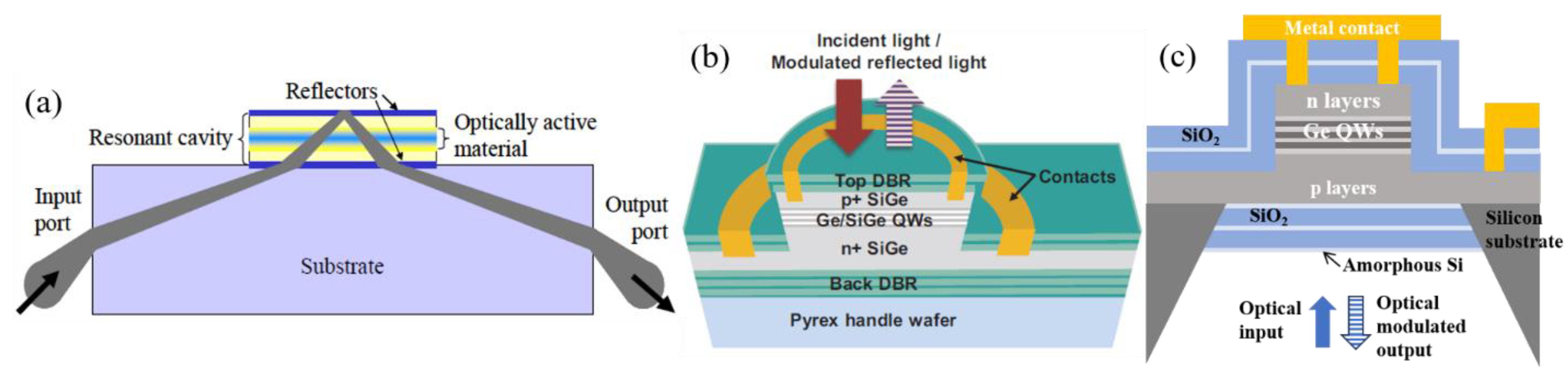
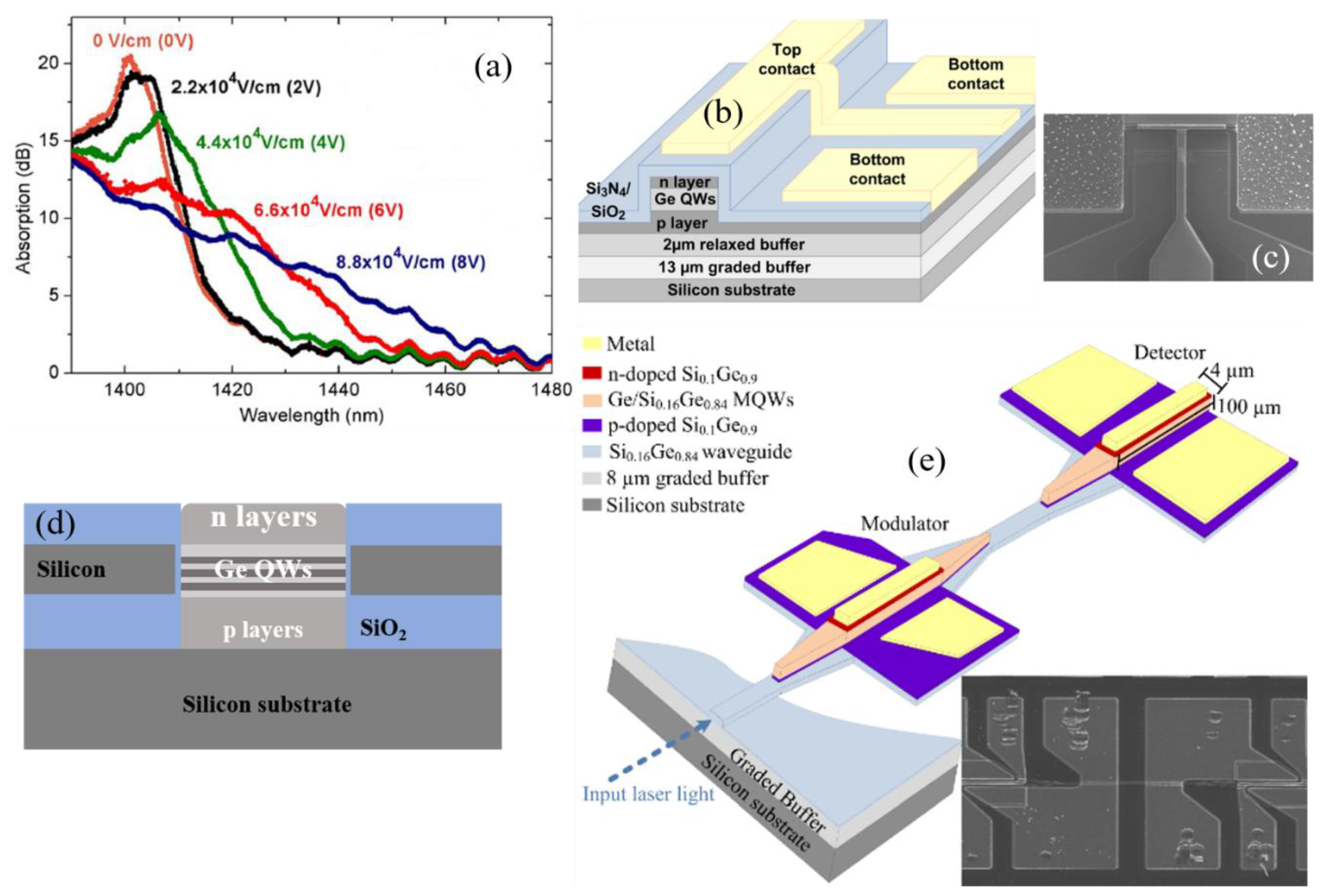
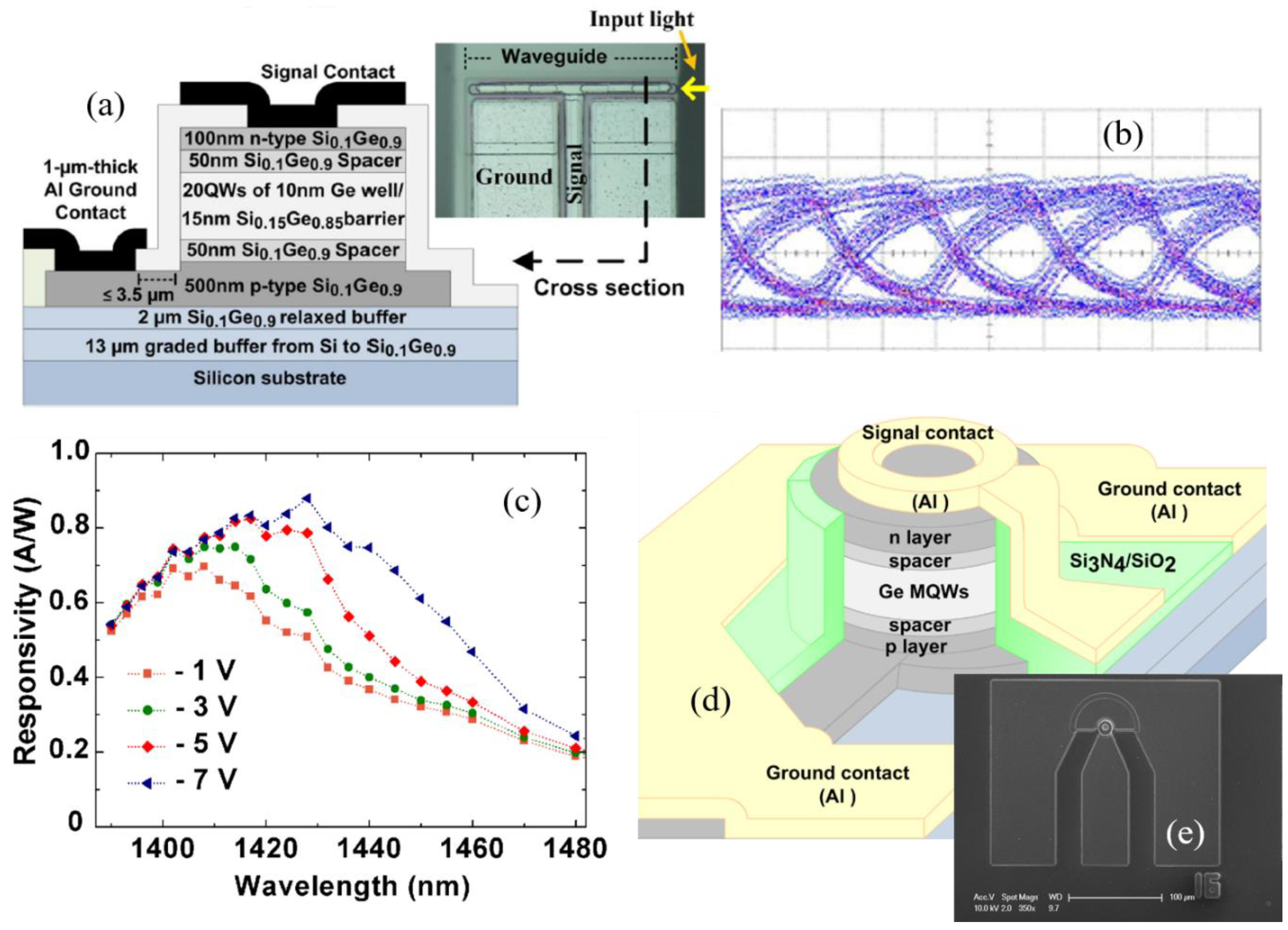
2. Ge/SiGe Quantum Well Optical Modulators

For optical interconnect applications, a compatible optical modulator should be able to meet several requirements, including: (1) a sufficiently-high extinction ratio (ER) (e.g., >5 dB ER [27]); (2) a relatively-low insertion loss (IL) (e.g., <3 dB IL [27]); (3) a complementary metal-oxide semiconductor (CMOS) drivable voltage (e.g., ≤2 V [32]); (4) a compact footprint and low-energy dissipation (e.g., <100 fJ/bit [5]); (5) CMOS-compatible materials and high-volume manufacturing compatibility; (6) a large 3-dB bandwidth for high-speed modulation (e.g., 14.3 GHz for on-chip clock in 2022 [5]); and (7) a relatively-large optical bandwidth (e.g., 10–20 nm [33]) for possible wavelength division multiplexing operation and a good temperature stability [34,35]. Several Si-compatible optical modulators have been proposed and investigated in order to demonstrate an optical modulator that can be manufactured by, and monolithically-integrated with, Si-microelectronics [33]. For Ge MQW optical modulators, QCSE properties have been experimentally investigated from O-band to C-band (1260–1550 nm) telecommunication wavelength regions.
After the discovery of QCSE using photocurrent measurement from strain-balanced Ge/SiGe QWs by Kuo et al. [18,19], Ge/SiGe MQW optical modulators have been reported in several configurations, including side entry, surface illumination, and waveguide configurations, as summarized in Table 1. As in Figure 1a, Roth et al. [36] reported transmission changes from Ge/SiGe QWs using a side-entry Ge/SiGe MQW modulator in 2007. Significant optical modulation could be obtained thanks to multiple reflections of light within an asymmetric Fabry-Perot resonator formed between the active regions of Ge/SiGe MQWs. A maximum ER of 7.3 dB at the optical wavelength of 1457 nm was measured with a voltage swing of 10 V (~4.8 × 10⁴ V/cm) between 0 V and 10 V; however, no information regarding the corresponding IL was obtained. Notably, by increasing the quality factor of the resonator and reducing the number of QWs, the side-entry Ge/SiGe MQW modulator could operate with a voltage swing of only 1 V (~1.5 × 10⁴ V/cm) between 3.6 V and 4.6 V for 3-dB ER [37]. For reference [37], the operating wavelength was redshifted to the C-band telecommunication wavelength at 1541 nm, as the authors characterized the modulator at 100 °C to match surface temperatures of high-performance CMOS chips. A semiconductor direct bandgap energy typically reduces with increasing temperature [38]. Kuo et al. [19] also reported the redshift of the Ge/SiGe MQW QCSE spectra in 2006 using photocurrent measurement.
For free-space optical interconnects [5], vertical-incidence Ge/SiGe MQW modulators were also of interest, thanks to their good thermal stability and lower susceptibility to crystalline defects as compared to directly-modulated VCSEL (Vertical-cavity surface-emitting laser) [5]. As in Figure 1b, Edwards et al. [39] reported in 2012 vertical-incidence Ge/SiGe MQW optical modulators, in which an asymmetric Fabry-Perot cavity of distributed Bragg reflector surrounding the Ge/SiGe MQWs was used to enhance modulation ER. The structure was designed such that the optical signal could be coupled into and out of the top surface of the device. At the operating wavelength of 1429 nm, the modulator exhibited 3.5 dB-ER with 3.7 dB-IL using a voltage swing of 3 V (~5.2 × 10⁴ V/cm) between 0.5 V and 3.5 V. As in Figure 1c, Audet et al. [40] in 2013 significantly improved the performance of vertical-incidence Ge/SiGe MQW optical modulators by employing an asymmetric Fabry-Perot resonant cavity made from high-index-contrast Bragg mirrors and reducing the number of QWs. Audet et al. achieved a good ER of 6.7 dB with a satisfactory IL of 4.1 dB at a swing bias voltage of 1 V (~2.2 × 10⁴ V/cm) between 5.5 V and 6.5 V. In addition, it is worth mentioning that Wei et al. [41] also theoretically proposed a vertical-incidence Ge QW asymmetric Fabry-Perot modulator without using a distributed Bragg reflector. They proposed that a cavity formed between a bottom metal on Si surface and the top SiGe/air interface could enhance optical modulation and predicted a competitive performance in terms of ER and IL. For the high-speed performance of vertical-incidence modulators, moderate values of 3-dB modulation bandwidth of 3–4 GHz obtained from [39,40,42] was expected to be due to the large diameter of the tested device, and expected to be circumvented by decreasing the device dimensions.
In 2011, as in Figure 2a, Chaisakul et al. investigated Ge/SiGe MQW modulators in a planar waveguide structure from 34-µm-long and 64-µm-long planar waveguides [43]. An input fiber was used to directly couple light into the tested device. A good performance of 10-dB ER and 5-dB IL was simultaneously obtained at the optical wavelength of 1428 nm for the device length of 64 µm, and the optical bandwidth, in which ER is more than 5 dB and IL is lower than 4 dB, is larger than 10 nm. Polarization-dependent absorption of Ge/SiGe MQWs was expected to play a role in the modulation performance of an optical modulator [44]. In 2013, Chaisakul et al. [45] demonstrated Ge/SiGe MQW optical modulators that use light hole related transitions at the Γ point (LH1-cΓ1), with the electric field perpendicular to the Ge QW plane instead of a heavy hole transition, with the electric field parallel to the Ge QW plane. The paper showed that a large and sharp optical absorption peak at the LH1-cΓ1 transition could be employed to improve the compactness of the modulators with competitive ER and IL values. In 2012, Chaisakul et al. [46] reported a 3-µm-wide and 90-µm-long Ge/SiGe MQW optical modulator, as shown in Figure 2b,c. The compact waveguide modulator can provide as high as 9-dB ER with a voltage swing of 1 V (~1.5 × 10⁴ V/cm) between 3 and 4 V at the optical wavelength of 1435 nm. At a longer optical wavelength of 1440 nm, 11-dB ER could be simultaneously obtained with 7.5-dB IL using a bias voltage of 5 V (~7.5 × 10⁴ V/cm). The optical modulator also exhibited a competitive 3-dB modulation bandwidth of 23 GHz. It is worth mentioning that Ge/SiGe MQW optical modulators give a comparable performance to III-V modulators in terms of ER performance at similar device length and applied electric field [47]. A higher IL of Ge/SiGe MQW optical modulators was a direct result of Ge indirect-gap absorption, which was experimentally and theoretically discussed in [48,49] by Schaevitz et al. and Kim et al., respectively. Interestingly, one could obtain higher values of electric fields inside the QWs by reducing the thickness of the Ge/SiGe MQW intrinsic region; therefore, high electric field contrasts could be obtained with small bias voltages [50].
For an operation within the O-band telecommunication wavelength, both Lever et al. [23] and Schaevitz et al. [27] predicted that it could be obtained by growing a strain-balanced Ge/Si0.4Ge0.6 MQW on the Si0.18Ge0.78 relaxed buffer. A buffer with a smaller lattice constant would increase the level of compressive strain applied to the Ge QWs, which would result in an increase in the optical bandgap of Ge QWs, and a blueshift of the operating optical wavelength. Additionally, Schaevitz et al. [27] also proposed that an addition of around 1% Si in the Ge QWs could also enable an O-band Ge/SiGe MQW optical modulator on a conventional Si0.10Ge0.90 relaxed buffer. Lever et al. [51] and Rouifed et al. [52] experimentally reported QCSE from photocurrent measurements around the optical wavelength of 1.3 µm using a similar structure of strain-balanced Ge/SiGe MQWs on Si0.22Ge0.78 and Si0.21Ge0.79 relaxed buffers, respectively. In 2014, Rouifed et al. [53] experimentally reported a 3-µm-wide and 50-µm-long Ge/SiGe MQW optical modulator operating in the O-band telecommunication wavelength. The modulator exhibited a 5-dB ER with 4-dB IL for a voltage swing of 3 V between 4 and 7 V at the optical wavelength of ~1295 nm. For the operation in the O-band optical wavelength range, the energy difference between the bottom of Γ- (local minimum of Ge conduction band at the zone center) and L- (global minimum of Ge conduction band) valley conduction band edges would become larger due to the additional compressive strain. As a result, it was expected that the absorption at L would become stronger compared to that at Γ, and the IL due to the L-valley indirect-gap absorption would become stronger, which could have a direct impact on both the obtainable ER and IL of an optical modulator [54]. Additionally, in 2014, Chaisakul et al. [55] experimentally demonstrated that O-band QCSE could also be obtained by simply decreasing the QW thickness, as in quantum well systems the optical bandgap would increase with decreasing QW width. As in Table 1, the waveguide modulator exhibited a good value of 8-dB ER simultaneously with 5-dB IL at the optical wavelength of 1345 nm for a 4-µm-wide and 100-µm-long Ge/SiGe MQW optical modulator integrated on a SiGe waveguide. It should be noted that in [55], the average Ge concentration of 6.5-nm Ge/10-nm Si0.15Ge0.85 MQWs was approximately 90%, equal to the Ge concentration of the relaxed layer on which the MQWs are grown; therefore, the structure was strain-balanced.
For operation within the C-band telecommunication wavelength, although only one Ge/SiGe MQW optical modulator in Table 1 was demonstrated via transmission measurements to have significant optical modulation in the C-band wavelength region [37], C-band QCSE was experimentally demonstrated and theoretically investigated by several researchers. Besides the method of increasing the temperature, C-band QCSE at room temperature was theoretically predicted by reducing the compressive strain in Ge QWs by using a relaxed buffer with a high Ge concentration [23], or decreasing the quantum confinement energy in Ge QWs by using relatively-thick Ge QWs [27,56]. Importantly, C-band QCSE was experimentally demonstrated by Edwards et al. [50] and Dumas et al. [57] from 14-nm thick Ge QWs via photocurrent measurements. It was also theoretically predicted that the application of 0.18–1.6% uniaxial tensile strain could enable C-band operation without using relatively-thick quantum wells [58,59]. On the other hand, it is possible to expect a Ge/SiGe electrorefraction optical modulator to operate optimally at a longer wavelength, as the modulator would utilize the variation of the refractive index in the absorption tail at the wavelength far from the absorption edge [60,61,62,63]. Experimentally, Frigerio et al. demonstrated electrorefraction within the optical wavelength from 1475 nm to 1520 nm with a VπLπ of as low as 0.46 V·cm at 1475 nm by using Ge/SiGe MQWs having an excitonic absorption at 1400 nm [61]. Moreover, Frigerio et al. also demonstrated electrorefraction with a VπLπ of as low as 0.046 V·cm at the optical wavelength of 1420 nm by using Ge/SiGe coupled MQWs with an excitonic absorption at 1370 nm [62].
A waveguide-integrated optical modulator is required in order to enable on-chip integration between different photonic devices. Lever et al. [64], Edwards et al. [50], and Rouifed et al. [53] theoretically studied evanescent coupling between the SOI waveguide and the Ge/SiGe MQWs. Although the taper section could be long (~100–300 µm) and increase the device footprint and optical absorption loss, a two-step taper was proposed to shorten the coupling length (~40–80 µm) in [64] and [53]. In 2012, Ren et al. theoretically studied [65] and experimentally demonstrated [66] an SOI-waveguide-integrated Ge/SiGe MQW optical modulator using a butt coupling approach, as shown in Figure 2d for example. The tested device had a very compact footprint of 8 µm2 and operated with only 1 V swing. Due to a mode mismatch between the submicron Si waveguide and relatively-thick Ge/SiGe MQW structures, high coupling loss was obtained. Butt coupling integration with a large core Si waveguide was experimentally investigated by Claussen et al. [67], which could be adopted for significantly-lower coupling loss. In 2014, Chaisakul et al. [68] demonstrated an evanescent coupling integration between a SiGe waveguide and Ge/SiGe MQWs using a 100-μm-long linear taper, as shown in Figure 2e. An ER of 3–4 dB was simultaneously obtained with 2–3 dB IL over 20 nm spectral ranges from 1430 to 1450 nm using a bias voltage swing between 0 and 3 V. Additionally, a low-voltage operation at 1 V and 2 V was also demonstrated. As a prospect toward reducing the taper length, in 2016, Zhou et al. [69] theoretically proposed a 45-μm-long taper coupler that can be used for polarization-insensitive optical coupling between a SiGe waveguide and Ge/SiGe MQWs. Regarding evanescent integration with the SOI waveguide, Zang et al. [70] recently reported in 2017 the development of an adiabatic 3D taper to assist the optical coupling between a SOI waveguide and Ge/SiGe MQW optical modulator. Theoretically, compared to a 2D taper, 3D taper gives a better coupling efficiency and improves the maintaining of the fundamental mode after coupling. Notably, another SOI waveguide integrated Ge/SiGe MQW optical modulator is also currently being developed [71].

3. Ge/SiGe Quantum Well Optical Detection and Emission

The possibility to employ the same QW structure for both optical modulation and detection can be highly beneficial for optical interconnect applications. For example, the excitonic absorption wavelength of Ge MQWs could be redshifted to a longer wavelength, at which the QCSE optical modulation is taking place, by applying a higher bias voltage similar to that used during a high-absorption mode of QCSE optical modulators. Alternatively, the same Ge/SiGe MQWs with different Ge QW optimal thickness values for optical modulator and photodetector could also be grown at the same time by using the local loading effect, depending on the growth window sizes [72,73]. This section summarizes the latest development regarding optical detection performance and emission characteristics obtained from the Ge/SiGe MQWs.

3.1. Optical Detection from Ge/SiGe MQWs

A high-performance photodetector should meet several requirements in terms of optical responsivities, dark currents, high speed performance, and footprint, as summarized in Table 2. In 2007, Fidaner et al. [74] reported a 3-µm-wide and 40-µm-long Ge/SiGe MQW waveguide detector with optical responsivity of 0.17 A/W at 1480 nm, which matched the optimum wavelength to obtain optical modulation based on QCSE of the same epitaxy; moreover, a data detection rate of 2.5 Gb/s at 8-V reverse bias was demonstrated. Fidaner et al. [74] attributed its low responsivity to low optical overlap between the optical mode and QWs, and suggested using a thinner buffer layer to increase optical overlap with Ge MQWs. Additionally, by employing a higher number of Ge MQW periods, optical overlap could be also improved. As shown in Figure 3a, Chaisakul et al. [75] reported a 3-µm-wide and 80-µm-long Ge/SiGe MQW waveguide detector with optical responsivity as high as 0.8 A/W that could operate up to 10 Gb/s at 3-V reverse bias, as in Figure 3b,c. Moreover, it was found that a reverse bias of only 1 V was enough to efficiently collect the photogenerated carriers at the excitonic wavelength of the Ge QW absorption. Besides a waveguide configuration, surface-illuminated photodiodes are also of interest for free space optical interconnects [5,76] or fiber-optic coupling applications. Thanks to a more relaxed optical coupling condition, a surface-illuminated photodiode is also ideal for investigating physical properties of new optoelectronic materials. Chaisakul et al. [77] experimentally reported high-speed operation of a 30-GHz 3-dB detection bandwidth from 12-µm-diameter surface-illuminated Ge/SiGe MQW photodiodes, as shown in Figure 3d,e. Additionally, by investigating the photodiodes with different diameter values of 50, 30, 20, 16 and 12 µm, the work established that the detection bandwidth of the larger diodes was limited by the RC time constant; however, for the smallest diodes the detection bandwidth limitation was due to Ge/SiGe MQW carrier dynamics that the carriers need to escape out of the QWs before reaching p- and n-doped regions [78,79]. As the early Ge/SiGe MQW photodetector operated optimally up to an optical wavelength of approximately 1500 nm, Onaran et al. [80] and Chang et al. [81] demonstrated the use of tensile strain to extend the optimal detection wavelength of the Ge/SiGe MQWs to be within the C-band wavelength region. The low responsivity values of 0.01 A/W at 1550 nm reported by Onaran et al. [80] from tested surfaced-illuminated photodiodes could be improved by increasing the number of MQW periods or by employing a waveguide configuration to increase the optical absorption length. For waveguide integration, Chaisakul et al. [68] demonstrated an optical responsivity as high as 1 A/W at 1-V reverse bias from a 4-µm-wide and 100-µm-long Ge/SiGe MQW waveguide photodetector integrated with a SiGe waveguide. In combination with a SiGe waveguide-integrated optical modulator, an optical interconnect was experimentally demonstrated on Si chip.
Additionally, it is worth mentioning that the reported responsivity and detection speed values from waveguide Ge/SiGe MQW photodetectors in Table 2 can be considered improvable as compared to the recent state-of-the-art Ge photodetector [13]. At a comparable intrinsic region thickness, Ge/SiGe MQWs would generally have less Ge absorbing layers, as the structures also contain SiGe barriers, which would contribute to a lower responsivity of Ge/SiGe MQW photodetectors at similar device thickness and bias voltage. For example, as compared to 0.74 A/W and 0.92 A/W obtained from 160-nm-thick Ge photodetector in [13], Chaisakul et al. [68] reported a slightly-lower responsivity of 0.6 A/W with 10 12-nm-thick Ge QWs, while [75] reported a comparable responsivity of 0.8 A/W with 20 10-nm-thick Ge QWs. For rapidity, the detection bandwidth of [68] was reported to be RC limited due to a relatively-large device dimension of 4 × 100 µm2 (~200 fF); therefore, high speed performance could be improved by optimizing the device dimensions.

3.2. Optical Emission from Ge/SiGe MQWs

Although being an indirect gap material, energy difference between Ge direct and indirect conduction band minima is very small (approximately 140 meV). As a result, the “quasi” direct-gap nature of Ge opens the possibility to engineer Ge direct-gap transition for optical emission, and optical gain around telecommunication wavelengths has been demonstrated from Ge direct-gap transition at room temperature [9,82]. Besides, the radiative recombination rate of Ge direct-gap optical transition is five orders of magnitude higher than that of the indirect one [83]. Therefore, as Ge direct-gap emission is expected to be strong, research efforts have been devoted to obtaining a population inversion at center of the Brillouin zone (Γ point) of Ge by the application of tensile strain to decrease the energy difference between the conduction band minima at Γ and L points, and by n-doping to fill the indirect-gap at L valleys. Both approaches would facilitate the injected electrons to occupy the higher energy states of the direct-gap at Γ point instead of the lower energy states of the indirect-gap at L valleys [84,85]. It is worth mentioning that a contradictory observation regarding the positive effect of n-type doping could also be found in [86].
An interest in investigating optical emission from QW structures is largely due to QW favorable density of states, which was used to achieve population inversion at a lower injected current density in III-V materials [87,88,89,90]. Additionally, QW structures could be engineered to have either transverse-electric (TE) or transverse-magnetic (TM) polarized optical emission [91]. For Ge QWs, Lange et al. [92] and Köster et al. [93] reported a transient optical gain from population inversion at Γ point observed from femtosecond time-resolved pump-probe spectroscopy. The transient population inversion was attributed to the fact that the intersubband relaxation of the optically-generated conduction band electrons is faster than their intravalley carrier-phonon scattering; τISB < τL-relax, as shown in Figure 4a [94].
Room temperature photoluminescence (PL) spectra of compressively-strained Ge MQWs were largely investigated. One of the first observations focused on the thermal excitation of carriers from L-type to Γ-type confined states, as reported by Gatti et al. [95] in 2011. As shown in Figure 4b, it resulted in an enhancement of PL spectra from direct-gap recombination of Ge MQWs at room temperature, compared to those at 5 K [95]. Compatible PL observations were also reported by Wu et al. [96] and Wei-Xuan et al. [97]. Additionally, an enhancement in optical emission at higher temperature was also observed from room temperature electroluminescence (EL). Chaisakul et al. [98] and Liu et al. [99] demonstrated in 2011 and 2012 an increase in EL intensity at higher temperature from compressively-strained Ge/SiGe MQW light emitting diodes, consistent with the PL observation. Additionally, for reference [98], the EL spectra were collected from the Ge/SiGe MQW light emitting diodes in a waveguide configuration. As in Figure 4c, EL from waveguide output facet was shown to have a TE polarization, confirming that it originated from the excitonic transition between the first valence band heavy hole level (HH1) and the first conduction band state at the Γ point (cΓ1), thanks to dipole selection rules in QW structures [100].
To further improve the emission efficiency, Cai et al. [101] theoretically proposed that tensile-strained Ge QWs instead of compressive-strained ones should be used to decrease the threshold current density needed for optical emission, thanks to the reduction of the energy difference between conduction band minima at Γ and L points. The application of tensile strain in Ge QWs had been proven by PL characterization results to be possible by several techniques, including the use of Ge virtual substrate [102,103,104], post-growth rapid thermal annealing [105], and SiNx stressor [106]. Notably, Gallacher et al. [107], Chao et al. [108], and Lin et al. [109] experimentally demonstrated room temperature EL from tensile-strained Ge/SiGe MQW light emitting diodes, with current injection current density as low as ~0.2 kA/cm2 for reference [107] and ~0.8 kA/cm2 for reference [109], which were lower than that of ~1.3 kA/cm2 obtained from compressive-strained Ge QWs of reference [98]. This difference could be considered agreeable with the theoretical prediction of ~50% from reference [101]. Moreover, as in Figure 4d, with the application of tensile strain on Ge QWs, the EL peak intensity due to the direct-gap transition at Γ valley was obtained around the C-band wavelength of 1550 nm. An increase in EL with increasing injection current density was clearly observed, and the EL intensity also increased with temperature, consistent with previous demonstration. It is worth noting that theoretically, Jiang et al. [110] have recently discussed the benefits of using QW structures to enhance optical emission in an indirect-band gap material, such as Ge. To further enhance the emission efficiency, the authors also recommended considering a GeSn/SiGeSn material system for a group IV quantum well laser.

4. Conclusions

The report of strong QCSE from the direct-gap transition of Ge/SiGe MQW systems has led to an ambitious quest toward realizing group IV quantum well optical modulators, photodetectors, and emitters from the same material platforms for more than ten years. For optical modulators, Ge/SiGe QCSE optical modulators have shown the capability to attain optical modulation comparable to III-V QW optical modulators at similar values of applied electrical fields, albeit at a cost of additional Ge indirect-gap absorption loss. Additionally, a demonstration of QCSE optical modulators that meet all the requirements of optical interconnect application at CMOS derivable voltage could be considered desirable. For photodetectors, at a comparable wavelength region of QCSE optical modulation, optical detection has been demonstrated from Ge/SiGe MQW photodetectors with an application of reverse bias voltages, as used during a high-absorption mode of QCSE optical modulators. Finally, the ambitious goal of a Ge/SiGe MQW platform appears to depend on the possibility to engineer the materials to emit light efficiently at room temperature. Although strenuous effort has been made, and a number of positive optical emission characteristics have been reported from Ge/SiGe MQWs, another group IV element of Sn may be considered indispensable to overcome the final hurdle of the ambitious objective.

Author Contributions

Writing—original draft preparation, P.C.; writing—review and editing, V.V., J.F., D.C. and D.M.M.; supervision, G.I., L.V. and D.M.M.

Funding

The Thailand Research Fund and the Office of the Higher Education Commission (Research Grant for New Scholar, MRG6180286). Kasetsart University Research and Development Institute (KURDI). The Faculty of Science, Kasetsart University (Preproposal Research Fund).

Conflicts of Interest

The authors declare no conflict of interest.

References

  1. Wada, K.; Kimerling, L.C. Photonics and Electronics with Germanium; Wiley-VCH Verlag GmbH & Co. KGaA: Weinheim, Germany, 2015. [Google Scholar]
  2. Miller, D.A.; Rationale, B. Challenges for Optical Interconnects to Electronic Chips. Proc. IEEE 2000, 88, 728–749. [Google Scholar] [CrossRef]
  3. Liu, J.; Camacho-Aguilera, R.; Bessette, J.T.; Sun, X.; Wang, X.; Cai, Y.; Kimerling, L.C.; Michel, J. Ge-on-Si optoelectronics. Thin Solid Films 2012, 520, 3354–3360. [Google Scholar] [CrossRef]
  4. Wang, X.; Liu, J. Emerging technologies in Si active photonics. J. Semicond. 2018, 39, 061001. [Google Scholar] [CrossRef]
  5. Miller, D.A.B. Device requirements for optical interconnects to silicon chips. Proc. IEEE 2009, 97, 1166–1185. [Google Scholar] [CrossRef]
  6. Liu, J.; Beals, M.; Pomerene, A.; Bernardis, S.; Sun, R.; Cheng, J.; Kimerling, L.C.; Michel, J. Waveguide-integrated, ultralow-energy GeSi electro-absorption modulators. Nat. Photonics 2008, 2, 433–437. [Google Scholar] [CrossRef]
  7. Assefa, S.; Xia, F.; Bedell, S.W.; Zhang, Y.; Topuria, T.; Rice, P.M.; Vlasov, Y.A. CMOS-integrated high-speed MSM germanium waveguide photodetector. Opt. Express 2010, 18, 4986–4999. [Google Scholar] [CrossRef] [PubMed]
  8. Feng, N.-N.; Feng, D.; Liao, S.; Wang, X.; Dong, P.; Liang, H.; Kung, C.-C.; Qian, W.; Fong, J.; Shafiiha, R.; et al. 30 GHz Ge electro-absorption modulator integrated with 3 μm silicon-on-insulator waveguide. Opt. Express 2011, 19, 7062–7067. [Google Scholar] [CrossRef] [PubMed]
  9. de Kersauson, M.M.; El Kurdi, D.S.; Checoury, X.; Fishman, G.; Sauvage, S.; Jakomin, R.; Beaudoin, G.; Sagnes, I.; Boucaud, P. Optical gain in single tensile-strained germanium photonic wire. Opt. Express 2011, 19, 17925–17934. [Google Scholar] [CrossRef] [PubMed]
  10. Vivien, L.; Polzer, A.; Marris-Morini, D.; Osmond, J.; Hartmann, J.M.; Crozat, P.; Cassan, E.; Kopp, C.; Zimmermann, H.; Fédéli, J.M. Zero-bias 40 Gbit/s germanium waveguide photodetector on silicon. Opt. Express 2012, 20, 1096–1101. [Google Scholar] [CrossRef] [PubMed]
  11. Camacho-Aguilera, R.E.; Cai, Y.; Patel, N.; Bessette, J.T.; Romagnoli, M.; Kimerling, L.C.; Michel, J. An electrically pumped germanium laser. Opt. Express 2012, 20, 11316–11320. [Google Scholar] [CrossRef] [PubMed]
  12. Srinivasan, A.; Verheyen, P.; Loo, R.; De Wolf, I.; Pantouvaki, M.; Lepage, G.; Balakrishnan, S.; Vanherle, W.; Absil, P.; Van Campenhout, J. 50 Gb/s C-band GeSi Waveguide Electro-Absorption Modulator. In Proceedings of the Optical Fiber Communication Conference (OFC), Anaheim, CA, USA, 20–24 March 2016; p. Tu3D.7. [Google Scholar]
  13. Chen, H.; Galili, M.; Verheyen, P.; De Heyn, P.; Lepage, G.; De Coster, J.; Balakrishnan, S.; Absil, P.; Oxenlowe, L.; Van Campenhout, J.; et al. 100-Gbps RZ data reception in 67-GHz Si-contacted germanium waveguide pin photodetectors. J. Lightwave Technol. 2017, 35, 722–726. [Google Scholar] [CrossRef]
  14. Cardona, M.; Pollak, F.H. Energy-band structure of germanium and silicon: The k·p method. Phys. Rev. 1966, 142, 530–543. [Google Scholar] [CrossRef]
  15. MacFarlane, G.G.; McLean, T.P.; Quarrington, J.E.; Roberts, V. Fine structure in the absorption-edge spectrum of Ge. Phys. Rev. 1957, 108, 1377–1383. [Google Scholar] [CrossRef]
  16. Dash, W.C.; Newman, R. Intrinsic Optical Absorption in Single-Crystal Germanium and Silicon at 77 K and 300 K. Phys. Rev. 1955, 99, 1151–1155. [Google Scholar] [CrossRef]
  17. Miller, D.A.B.; Chemla, D.S.; Damen, T.C.; Gossard, A.C.; Wiegmann, W.; Wood, T.H.; Burrus, C.A. Band-edge electroabsorption in quantum well structures: The quantum-confined Stark effect. Phys. Rev. Lett. 1984, 53, 2173. [Google Scholar] [CrossRef]
  18. Kuo, Y.-H.; Lee, Y.K.; Ge, Y.; Ren, S.; Roth, J.E.; Kamins, T.I.; Miller, D.A.B.; Harris, J.S. Strong quantum-confined Stark effect in a germanium quantum-well structures on silicon. Nature 2005, 437, 1334–1336. [Google Scholar] [CrossRef] [PubMed]
  19. Kuo, Y.-H.; Lee, Y.K.; Ge, Y.; Ren, S.; Roth, J.E.; Kamins, T.I.; Miller, D.A.B.; Harris, J.S., Jr. Quantum-confined stark effect in Ge/SiGe quantum wells on Si for optical modulators. IEEE J. Sel. Top. Quantum Electron. 2006, 12, 1503–1513. [Google Scholar] [CrossRef]
  20. Schaevitz, R.K.; Roth, J.E.; Member, R.S.; Fidaner, O.; Miller, D.A.B. Material Properties of Si-GeGe Quantum Wells. IEEE J. Sel. Top. Quantum Electron. 2008, 14, 1082–1089. [Google Scholar] [CrossRef]
  21. Virgilio, M.; Grosso, G. Quantum-confined Stark effect in Ge/SiGe quantum wells: A tight-binding description. Phys. Rev. B 2008, 77, 165315. [Google Scholar] [CrossRef]
  22. Paul, D.J. 8-band k.p modelling of the quantum confined Stark effect in Ge quantum wells on Si substrates. Phys. Rev. B 2008, 77, 155323. [Google Scholar] [CrossRef]
  23. Lever, L.; Ikonic, Z.; Valavanis, A.; Cooper, J.; Kelsall, R. Design of Ge-SiGe quantum-confined Stark effect electroabsorption heterostructures for CMOS compatible photonics. J. Lightwave Technol. 2010, 28, 3273–3281. [Google Scholar] [CrossRef]
  24. Busby, Y.; De Seta, M.; Capellini, G.; Evangelisti, F.; Ortolani, M.; Virgilio, M.; Grosso, G.; Pizzi, G.; Calvani, P.; Lupi, S.; et al. Near- and far-infrared absorption and electronic structure of Ge-SiGe multiple quantum wells. Phys. Rev. B 2010, 82, 205317. [Google Scholar] [CrossRef]
  25. Kuo, Y.-H.; Li, Y.-S. Direct-gap exciton and optical absorption in the Ge/SiGe quantum well system. Appl. Phys. Lett. 2009, 94, 121101. [Google Scholar] [CrossRef]
  26. Kuo, Y.-H.; Li, Y.-S. Variational calculation for the direct-gap exciton in the Ge quantum well systems. Phys. Rev. B 2009, 79, 245328. [Google Scholar] [CrossRef]
  27. Schaevitz, R.K.; Edwards, E.H.; Roth, J.E.; Fei, E.T.; Rong, Y.; Wahl, P.; Kamins, T.I.; Harris, J.S.; Miller, D.A.B. Simple electroabsorption calculator for designing 1310 nm and 1550 nm modulators using germanium quantum wells. IEEE J. Quantum Electron. 2012, 48, 187–197. [Google Scholar] [CrossRef]
  28. Tsujino, S.; Sigg, H.; Mussler, G.; Chrastina, D.; von Känel, H. Photocurrent and transmission spectroscopy of direct-gap interband transitions in Ge/SiGe quantum wells. Appl. Phys. Lett. 2006, 89, 262119. [Google Scholar] [CrossRef]
  29. Bonfanti, M.; Grilli, E.; Guzzi, M.; Chrastina, D.; Isella, G.; von Känel, H.; Sigg, H. Direct-gap related optical transitions in Ge/SiGe quantum wells with Ge-rich barriers. Physica E 2009, 41, 972–975. [Google Scholar] [CrossRef]
  30. Chaisakul, P.; Marris-Morini, D.; Isella, G.; Chrastina, D.; Le Roux, X.; Gatti, E.; Edmond, S.; Osmond, J.; Cassan, E.; Vivien, L. Quantum-confined Stark effect measurements in Ge/SiGe quantum-well structures. Opt. Lett. 2010, 35, 2913–2915. [Google Scholar] [CrossRef] [PubMed]
  31. Isella, G.; Chrastina, D.; Rössner, B.; Hackbarth, T.; Herzog, H.-J.; König, U.; von Känel, H. Low-energy plasma-enhanced chemical vapor deposition for strained Si and Ge heterostructures and devices. Solid-State Electron. 2004, 48, 1317–1323. [Google Scholar] [CrossRef]
  32. Thomson, D.; Zilkie, A.; Bowers, J.E.; Komljenovic, T.; Reed, G.T.; Vivien, L.; Marris-Morini, D.; Cassan, E.; Virot, L.; Fédéli, J.-M.; et al. Roadmap on silicon photonics. J. Opt. 2016, 18, 073003. [Google Scholar] [CrossRef]
  33. Reed, G.T.; Mashanovich, G.; Gardes, F.Y.; Thomson, D.J. Silicon optical modulators. Nat. Photon. 2010, 4, 518–526. [Google Scholar] [CrossRef]
  34. Zhang, Z.; Yako, M.; Ju, K.; Kawai, N.; Chaisakul, P.; Tsuchizawa, T.; Hikita, M.; Yamada, K.; Ishikawa, Y.; Wada, K. A new material platform of Si photonics for implementing architecture of dense wavelength division multiplexing on Si bulk wafer. Sci. Technol. Adv. Mater. 2017, 18, 283–293. [Google Scholar] [CrossRef] [PubMed]
  35. Kekatpure, R.D.; Lentine, A. The suitability of SiGe multiple quantum well modulators for short reach DWDM optical interconnects. Opt. Express 2013, 21, 5318–5331. [Google Scholar] [CrossRef] [PubMed]
  36. Roth, J.E.; Fidaner, O.; Schaevitz, R.K.; Kuo, Y.-H.; Kamins, T.I.; Harris, J.S.; Miller, D.A.B. Optical modulator on silicon employing germanium quantum wells. Opt. Express 2007, 15, 5851–5859. [Google Scholar] [CrossRef] [PubMed]
  37. Roth, J.E.; Fidaner, O.; Englund, E.E.; Schaevitz, R.K.; Kuo, Y.-H.; Helman, N.C.; Kamins, T.I.; Harris, J.S.; Miller, D.A.B. C-band side-entry Ge quantum well electroabsorption modulator on SOI operating at 1 volt swing. Electron. Lett. 2008, 44, 49–50. [Google Scholar] [CrossRef]
  38. Sze, S.M.; Ng, K.K. Physics of Semiconductor Devices, 3rd ed.; Wiley-Interscience: Hoboken, NJ, USA, 2006. [Google Scholar]
  39. Edwards, E.H.; Audet, R.M.; Fei, E.T.; Claussen, S.A.; Schaevitz, R.K.; Tasyurek, E.; Rong, Y.; Kamins, T.I.; Harris, J.S.; Miller, D.A.B. Ge/SiGe asymmetric Fabry-Perot quantum well electroabsorption modulators. Opt. Express 2012, 20, 29164–29173. [Google Scholar] [CrossRef] [PubMed]
  40. Audet, R.M.; Edwards, E.H.; Balram, K.C.; Claussen, S.A.; Schaevitz, R.K.; Tasyurek, E.; Rong, Y.; Fei, E.I.; Kamins, T.I.; Harris, J.S.; et al. Surface-normal ge/sige asymmetric fabry-perot optical modulators fabricated on silicon substrates. J. Lightwave Technol. 2013, 31, 3995–4003. [Google Scholar] [CrossRef]
  41. Wei, Y.-P.; Kuo, Y.-H. Design of vertical Ge quantum well asymmetric Fabry-Perot modulator without DBR. Opt. Express 2010, 18, 23576–23583. [Google Scholar] [CrossRef] [PubMed]
  42. Rong, Y.; Ge, Y.; Huo, Y.; Fiorentino, M.; Tan, M.R.T.; Kamins, T.I.; Ochalski, T.J.; Huyet, G.; Harris, J.S., Jr. Quantum-confined Stark effect in Ge/SiGe quantum wells on Si. IEEE J. Sel. Top. Quantum Electron. 2010, 16, 85–92. [Google Scholar] [CrossRef]
  43. Chaisakul, P.; Marris-Morini, D.; Isella, G.; Chrastina, D.; Le Roux, X.; Edmond, S.; Coudevylle, J.-R.; Cassan, E.; Vivien, L. Polarization dependence of quantum-confined Stark effect in Ge/SiGe quantum well planar waveguides. Opt. Lett. 2011, 36, 1794–1796. [Google Scholar] [CrossRef] [PubMed]
  44. Virgilio, M.; Bonfanti, M.; Chrastina, D.; Neels, A.; Isella, G.; Grilli, E.; Guzzi, M.; Grosso, G.; Sigg, H.; von Känel, H. Polarization-dependent absorption in Ge/SiGe multiple quantum wells: Theory and experiment. Phys. Rev. B 2009, 79, 075323. [Google Scholar] [CrossRef]
  45. Chaisakul, P.; Marris-Morini, D.; Rouifed, M.S.; Frigerio, J.; Isella, G.; Chrastina, D.; Coudevylle, J.R.; Le Roux, X.; Edmond, S.; Bouville, D.; et al. Strong quantum-confined Stark effect from light hole related direct-gap transitions in Ge quantum wells. Appl. Phys. Lett. 2013, 102, 191107. [Google Scholar] [CrossRef]
  46. Chaisakul, P.; Marris-Morini, D.; Rouifed, M.-S.; Isella, G.; Chrastina, D.; Frigerio, J.; Le Roux, X.; Edmond, S.; Coudevylle, J.-R.; Vivien, L. 23 GHz Ge/SiGe multiple quantum well electro-absorption modulator. Opt. Express 2012, 20, 3219–3224. [Google Scholar] [CrossRef] [PubMed]
  47. Kuo, Y.-H.; Chen, H.-W.; Bowers, J.E. High speed hybrid silicon evanescent electroabsorption modulator. Opt. Express 2008, 16, 9936–9941. [Google Scholar] [CrossRef] [PubMed]
  48. Schaevitz, R.K.; Ly-Gagnon, D.S.; Roth, J.E.; Edwards, E.H.; Miller, D.A.B. Indirect absorption in germanium quantum wells. AIP Adv. 2011, 1, 032164. [Google Scholar] [CrossRef]
  49. Kim, J.; Ahn, D. Effect of indirect interband absorption in Ge/SiGe quantum wells. J. Appl. Phys. 2011, 110, 083119. [Google Scholar] [CrossRef]
  50. Edwards, E.H.; Lever, L.; Fei, E.T.; Kamins, T.I.; Ikonic, Z.; Harris, J.S.; Kelsall, R.W.; Miller, D.A.B. Low-voltage broad-band electroabsorption from thin Ge/SiGe quantum wells epitaxially grown on silicon. Opt. Express 2013, 21, 867–876. [Google Scholar] [CrossRef] [PubMed]
  51. Lever, L.; Hu, Y.; Myronov, M.; Liu, X.; Owens, N.; Gardes, F.Y.; Marko, I.P.; Sweeney, S.J.; Ikonić, Z.; Leadley, D.R.; et al. Modulation of the absorption coefficient at 1.3 μm in Ge/SiGe multiple quantum well heterostructures on silicon. Opt. Lett. 2011, 36, 4158–4160. [Google Scholar] [CrossRef] [PubMed]
  52. Rouifed, M.S.; Chaisakul, P.; Marris-Morini, D.; Frigerio, J.; Isella, G.; Chrastina, D.; Edmond, S.; Le Roux, X.; Coudevylle, J.-R.; Vivien, L. Quantum-confined Stark effect at 1.3 μm in Ge/Si0.35Ge0.65 quantum-well structure. Opt. Lett. 2012, 37, 3960–3962. [Google Scholar] [CrossRef] [PubMed]
  53. Rouifed, M.S.; Marris-Morini, D.; Chaisakul, P.; Frigerio, J.; Isella, G.; Chrastina, D.; Edmond, S.; Le Roux, X.; Coudevylle, J.R.; Bouville, D.; et al. Advances Toward Ge/SiGe Quantum-Well Waveguide Modulators at 1.3 μm. IEEE J. Sel. Top. Quantum Electron. 2014, 20, 33–39. [Google Scholar] [CrossRef]
  54. Chaisakul, P.; Marris-Morini, D.; Rouifed, M.-S.; Frigerio, J.; Chrastina, D.; Coudevylle, J.-R.; Le Roux, X.; Edmond, S.; Isella, G.; Vivien, L. Recent progress in GeSi electro-absorption modulators. Sci. Technol. Adv. Mater. 2014, 15, 014601. [Google Scholar] [CrossRef] [PubMed]
  55. Chaisakul, P.; Frigerio, J.; Marris-Morini, D.; Vakarin, V.; Chrastina, D.; Isella, G.; Vivien, L. O-band quantum-confined Stark effect optical modulator from Ge/SiGe quantum wells by well thickness tuning. J. Appl. Phys. 2014, 116, 193103. [Google Scholar] [CrossRef]
  56. Gao, J.; Zhou, H.; Jiang, J.; Zhou, Y.; Sun, J. Design of low bias voltage Ge/SiGe multiple quantum wells electro-absorption modulator at 1550 nm. AIP Adv. 2017, 7, 035317. [Google Scholar] [CrossRef]
  57. Dumas, D.C.S.; Gallacher, K.; Rhead, S.; Myronov, M.; Leadley, D.R.; Paul, D.J. Ge/SiGe quantum confined Stark effect electro-absorption modulation with low voltage swing at λ = 1550 nm. Opt. Express 2014, 22, 19284–19292. [Google Scholar] [CrossRef] [PubMed]
  58. Chang, G.-E.; Chang, C.-O. Tensile-Strained Ge/SiGeSn Quantum Wells for Polarization-Insensitive Electro-Absorption Waveguide Modulators. IEEE J. Quantum Electron. 2012, 48, 533–541. [Google Scholar] [CrossRef]
  59. Gao, J.; Sun, J.; Jiang, J.; Zhou, H.; Zhou, Y. Design and analysis of electro-absorption modulators with uniaxially stressed Ge/SiGe multiple quantum wells. Opt. Express 2017, 25, 10874–10884. [Google Scholar] [CrossRef] [PubMed]
  60. Iseri, Y.; Yamada, H.; Goda, Y.; Arakawa, T.; Tada, K.; Haneji, N. Analysis of electrorefractive index change in Ge/SiGe coupled quantum well for low-voltage silicon-based optical modulators. Phys. E 2011, 43, 1433–1438. [Google Scholar] [CrossRef]
  61. Frigerio, J.; Chaisakul, P.; Marris-Morini, D.; Cecchi, S.; Rouifed, M.-S.; Isella, G.; Vivien, L. Electro-Refractive Effect in Ge/SiGe Multiple Quantum Wells. Appl. Phys. Lett. 2013, 102, 061102. [Google Scholar] [CrossRef]
  62. Frigerio, J.; Vakarin, V.; Chaisakul, P.; Ferretto, M.; Chrastina, D.; Le Roux, X.; Vivien, L.; Isella, G.; Marris-Morini, D. Giant electro-optic effect in Ge/SiGe coupled quantum wells. Sci. Rep. 2015, 5, 15398. [Google Scholar] [CrossRef] [PubMed]
  63. Zhang, Y.; Sun, J.; Gao, J. Theoretical analysis of electro-refractive index variation in asymmetric Ge/SiGe coupled quantum wells. Opt. Express 2017, 25, 30032–30042. [Google Scholar] [CrossRef] [PubMed]
  64. Lever, L.; Ikonić, Z.; Kelsall, R.W. Adiabatic mode coupling between SiGe photonic devices and SOI waveguides. Opt. Express 2012, 20, 29500–29506. [Google Scholar] [CrossRef] [PubMed]
  65. Ren, S.; Kamins, T.I.; Miller, D.A.B. Thin dielectric spacer for the monolithic integration of bulk germanium or germanium quantum wells with silicon-on-insulator waveguides. IEEE Photonics J. 2011, 3, 739–747. [Google Scholar] [CrossRef]
  66. Ren, S.; Rong, Y.; Claussen, S.A.; Schaevitz, R.K.; Kamins, T.I.; Harris, J.S.; Miller, D.A.B. Ge/SiGe quantum well waveguide modulator monolithically integrated with SOI waveguides. IEEE Photonics Technol. Lett. 2012, 24, 461–463. [Google Scholar] [CrossRef]
  67. Claussen, S.A.; Balram, K.C.; Fei, E.T.; Kamins, T.I.; Harris, J.S.; Miller, D.A.B. Selective area growth of germanium and germanium/silicon-germanium quantum wells in silicon waveguides for on-chip optical interconnect applications. Opt. Mater. Express 2012, 2, 1336–1342. [Google Scholar] [CrossRef]
  68. Chaisakul, P.; Marris-Morini, D.; Frigerio, J.; Chrastina, D.; Rouifed, M.-S.; Cecchi, S.; Crozat, P.; Isella, G.; Vivien, L. Integrated germanium optical interconnects on silicon substrates. Nat. Photonics 2014, 8, 482–488. [Google Scholar] [CrossRef]
  69. Zhou, H.; Sun, J.; Gao, J.; Jiang, J.; Zhou, Y. Design of compact and efficient polarization-insensitive taper coupler for SiGe photonic integration. Opt. Express 2016, 24, 23784–23797. [Google Scholar] [CrossRef] [PubMed]
  70. Zang, K.; Lu, C.-Y.; Chen, X.; Fei, E.; Xue, M.; Claussen, S.; Morea, M.; Chen, Y.; Dutt, R.; Huo, Y.; et al. Germanium Quantum Well QCSE Waveguide Modulator with Tapered Coupling in Distributed Modulator–Detector System. J. Lightwave Technol. 2017, 35, 4629–4633. [Google Scholar] [CrossRef]
  71. Srinivasan, S.A.; Porret, C.; Vissers, E.; Geiregat, P.; Van Thourhout, D.; Loo, R.; Pantouvaki, M.; Van Campenhout, J. High-contrast quantum-confined Stark effect in Ge/SiGe quantum well stacks on Si with ultra-thin buffer layers. In Proceedings of the Conference on Lasers and Electro-Optics/Pacific Rim 2018, Hong Kong, China, 29 July–3 August 2018. [Google Scholar]
  72. Kamins, T.I. Pattern sensitivity of selective Si1−xGex chemical vapor deposition: Pressure dependence. J. Appl. Phys. 1993, 74, 5799–5802. [Google Scholar] [CrossRef]
  73. Ren, S.; Rong, Y.; Kamins, T.I.; Harris, J.S.; Miller, D.A.B. Selective epitaxial growth of Ge/Si0.15Ge0.85 quantum wells on Si substrate using reduced pressure chemical vapor deposition. Appl. Phys. Lett. 2011, 98, 151108. [Google Scholar]
  74. Fidaner, O.; Okyay, A.K.; Roth, J.E.; Schaevitz, R.K.; Kuo, Y.-H.; Saraswat, K.C.; Harris, J.S.; Miller, D.A.B. Ge-SiGe quantum-well waveguide photodetectors on silicon for the near-infrared. IEEE Photonics Technol. Lett. 2007, 19, 1631–1633. [Google Scholar] [CrossRef]
  75. Chaisakul, P.; Marris-Morini, D.; Isella, G.; Chrastina, D.; Rouifed, M.-S.; Le Roux, X.; Edmond, S.; Cassan, E.; Coudevylle, J.-R.; Vivien, L. 10-Gb/s Ge/SiGe Multiple Quantum-Well Waveguide Photodetector. IEEE Photonic Technol. Lett. 2011, 23, 1430–1432. [Google Scholar] [CrossRef]
  76. Miller, D.A.B. Optical interconnects to electronic chips. Appl. Opt. 2010, 49, F59–F70. [Google Scholar] [CrossRef] [PubMed]
  77. Chaisakul, P.; Marris-Morini, D.; Isella, G.; Chrastina, D.; Le Roux, X.; Edmond, S.; Cassan, E.; Coudevylle, J.-R.; Vivien, L. Ge/SiGe multiple quantum well photodiode with 30 GHz bandwidth. Appl. Phys. Lett. 2011, 98, 131112. [Google Scholar] [CrossRef]
  78. Giorgioni, A.; Gatti, E.; Grilli, E.; Chernikov, A.; Chatterjee, S.; Chrastina, D.; Isella, G.; Guzzi, M. Photoluminescence decay of direct and indirect transitions in Ge/SiGe multiple quantum wells. J. Appl. Phys. 2012, 111, 013501. [Google Scholar] [CrossRef]
  79. Claussen, S.A.; Tasyurek, E.; Roth, J.E.; Miller, D.A. Measurement and modeling of ultrafast carrier dynamics and transport in germanium/silicon-germanium quantum wells. Opt. Express 2010, 18, 25596–25607. [Google Scholar] [CrossRef] [PubMed]
  80. Onaran, E.; Onbasli, M.C.; Yesilyurt, A.; Yu, H.Y.; Nayfeh, A.M.; Okyay, A.K. Silicon-Germanium multi-quantum well photodetectors in the near infrared. Opt. Express 2012, 20, 7608–7615. [Google Scholar] [CrossRef] [PubMed]
  81. Chang, G.-E.; Chen, S.-W.; Cheng, H.H. Tensile-strained Ge/SiGe quantum-well photodetectors on silicon substrates with extended infrared response. Opt. Express 2016, 24, 17562–17571. [Google Scholar] [CrossRef] [PubMed]
  82. Liu, J.; Sun, X.; Kimerling, L.C.; Michel, J. Direct-gap optical gain of Ge on Si at room temperature. Opt. Lett. 2009, 34, 1738–1740. [Google Scholar] [CrossRef] [PubMed]
  83. Haynes, J.R.; Nilsson, N.G. Physics of Semiconductors: Proceedings of the VIIth International Conference; Dunod: Paris, France, 1964; p. 21. [Google Scholar]
  84. Liu, J.; Sun, X.; Pan, D.; Wang, X.; Kimerling, L.C.; Koch, T.L.; Michel, J. Tensile-strained, n-type Ge as a gain medium for monolithic laser integration on Si. Opt. Express 2007, 15, 11272–11277. [Google Scholar] [CrossRef] [PubMed]
  85. Liu, J.; Sun, X.; Camacho-Aguilera, R.; Kimerling, L.C.; Michel, J. Ge-on-Si laser operating at room temperature. Opt. Lett. 2010, 35, 679–681. [Google Scholar] [CrossRef] [PubMed]
  86. Carroll, L.; Friedli, P.; Neuenschwander, S.; Sigg, H.; Cecchi, S.; Isa, F.; Chrastina, D.; Isella, G.; Fedoryshyn, Y.; Faist, J. Direct-gap gain and optical absorption in Germanium correlated to the density of photoexcited carriers, doping, and strain. Phys. Rev. Lett. 2012, 109, 057402. [Google Scholar] [CrossRef] [PubMed]
  87. Iga, K.; Koyama, F.; Konoshita, S. Surface emitting semiconductor lasers. IEEE J. Quantum Electron. 1988, 24, 1845–1855. [Google Scholar] [CrossRef]
  88. Jewell, J.L.; Scherer, A.; McCall, S.L.; Lee, Y.H.; Walker, S.; Harbison, J.P.; Florez, L.T. Low-threshold electrically pumped vertical-cavity surface-emitting microlasers. Electron. Lett. 1989, 25, 1123–1124. [Google Scholar] [CrossRef]
  89. Steinmann, P.; Borchert, B.; Stegmuller, B. Improved behavior of monolithically integrated laser/modulator by modified identical active layer structure. IEEE Photonics Technol. Lett. 1997, 9, 1561–1563. [Google Scholar] [CrossRef]
  90. Kobayashi, W.; Arai, M.; Yamanaka, T.; Fujiwara, N.; Fujisawa, T.; Tadokoro, T.; Tsuzuki, K.; Kondo, Y.; Kano, F. Design and Fabrication of 10-/40-Gb/s, Uncooled Electroabsorption Modulator Integrated DFB Laser with Butt-Joint Structure. J. Lightwave Technol. 2010, 28, 164–171. [Google Scholar] [CrossRef]
  91. Jones, G.; Smith, A.D.; O’Reilly, E.P.; Silver, M.; Briggs, A.T.R.; Fice, M.J.; Adams, A.R.; Greene, P.D.; Scarrott, K.; Vranic, A. The influence of tensile strain on differential gain and auger recombination in 1.5-μm multiple-quantum-well lasers. IEEE J. Quantum Electron. 1998, 34, 822–833. [Google Scholar] [CrossRef]
  92. Lange, C.; Köster, N.S.; Chatterjee, S.; Sigg, H.; Chrastina, D.; Isella, G.; von Känel, H.; Schäfer, M.; Kira, M.; Koch, S.W. Ultrafast nonlinear optical response of photoexcited Ge/SiGe quantum wells: Evidence for a femtosecond transient population inversion. Phys. Rev. B 2009, 79, 201306. [Google Scholar] [CrossRef]
  93. Köster, N.S.; Lange, C.; Kolata, K.; Chatterjee, S.; Schäfer, M.; Kira, M.; Koch, S.W.; Chrastina, D.; Isella, G.; von Känel, H.; et al. Ultrafast transient gain in Ge/SiGe quantum wells. Phys. Status Solidi C 2011, 8, 1109–1112. [Google Scholar] [CrossRef]
  94. Gatti, E.; Grilli, E.; Guzzi, M.; Chrastina, D.; Isella, G.; Chernikov, A.; Bornwasser, V.; Köster, N.; Woscholski, R.; Chatterjee, S. Photoluminescence and ultrafast inter-subband relaxation in Ge/SiGe multiple quantum wells. Phys. Rev. B 2011, 84, 245319. [Google Scholar] [CrossRef]
  95. Gatti, E.; Grilli, E.; Guzzi, M.; Chrastina, D.; Isella, G.; von Känel, H. Room temperature photoluminescence of Ge multiple quantum wells with Ge-rich barriers. Appl. Phys. Lett. 2011, 98, 031106. [Google Scholar] [CrossRef]
  96. Wu, P.H.; Dumcenco, D.; Huang, Y.S.; Hsu, H.P.; Lai, C.H.; Lin, T.Y.; Chrastina, D.; Isella, G.; Gatti, E.; Tiong, K.K. Above-room-temperature photoluminescence from a strain-compensated Ge/Si0.15Ge0.85 multiple-quantum-well structure. Appl. Phys. Lett. 2012, 100, 141905. [Google Scholar] [CrossRef]
  97. Hu, W.; Cheng, B.; Xue, C.; Zhang, G.; Su, S.; Zuo, Y.; Wang, Q. Room-temperature direct-bandgap photoluminescence from strain-compensated Ge/SiGe multiple quantum wells on silicon. Chin. Phys. B 2012, 21, 017805. [Google Scholar] [CrossRef]
  98. Chaisakul, P.; Marris-Morini, D.; Isella, G.; Chrastina, D.; Izard, N.; Le Roux, X.; Edmond, S.; Coudevylle, J.-R.; Vivien, L. Room temperature direct gap electroluminescence from Ge/Si0.15Ge0.85 multiple quantum well waveguide. Appl. Phys. Lett. 2011, 99, 141106. [Google Scholar] [CrossRef]
  99. Liu, Z.; Hu, W.; Li, C.; Li, Y.; Xue, C.; Li, C.; Zuo, Y.; Chenga, B.; Wang, Q. Room temperature direct-bandgap electroluminescence from n-type strain-compensated Ge/SiGe multiple quantum wells. Appl. Phys. Lett. 2012, 101, 231108. [Google Scholar] [CrossRef]
  100. Bastard, G. Wave Mechanics Applied to Semiconductor Heterostructures; Halstead Press: New York, NY, USA, 1988. [Google Scholar]
  101. Cai, Y.; Han, Z.; Wang, X.; Camacho-Aguilera, R.E.; Kimerling, L.C.; Michel, J.; Liu, J. Analysis of Threshold Current Behavior for Bulk and Quantum-Well Germanium Laser Structures. IEEE J. Sel. Top. Quantum Electron. 2013, 19, 1901009. [Google Scholar]
  102. Chen, Y.; Li, C.; Zhou, Z.; Lai, H.; Chen, S.; Ding, W.; Cheng, B.; Yu, Y. Room temperature photoluminescence of tensile-strained Ge/Si0.13Ge0.87 quantum wells grown on silicon-based germanium virtual substrate. Appl. Phys. Lett. 2009, 94, 141902. [Google Scholar] [CrossRef]
  103. Chen, Y.; Li, C.; Lai, H.; Chen, S. Quantum-confined direct band transitions in tensile strained Ge/SiGe quantum wells on silicon substrates. Nanotechnology 2010, 21, 115207. [Google Scholar] [CrossRef] [PubMed]
  104. Carroll, L.; Imbert, F.; Sigg, H.; Süess, M.; Müller, E.; Virgilio, M.; Pizzi, G.; Rossbach, P.; Chrastina, D.; Isella, G. Quantum-confined direct-gap transitions in tensile-strained Ge/SiGe multiple quantum wells. Appl. Phys. Lett. 2011, 99, 031907. [Google Scholar] [CrossRef]
  105. Süess, M.J.; Carroll, L.; Sigg, H.; Diaz, A.; Chrastina, D.; Isella, G.; Müller, E.; Spolenak, R. Tensile strained Ge quantum wells on Si substrate: Post-growth annealing versus low temperature re-growth. Mater. Sci. Eng. B 2012, 177, 696–699. [Google Scholar] [CrossRef]
  106. Chen, X.; Fenrich, C.S.; Xue, M.; Kao, M.-Y.; Zang, K.; Lu, C.-Y.; Fei, E.T.; Chen, Y.; Huo, Y.; Kamins, T.I.; et al. Tensile-strained Ge/SiGe multiple quantum well microdisks. Photonics Res. 2017, 5, B7–B14. [Google Scholar] [CrossRef]
  107. Gallacher, K.; Velha, P.; Paul, D.J.; Cecchi, S.; Frigerio, J.; Chrastina, D.; Isella, G. 1.55 μm direct bandgap electroluminescence from strained n-Ge quantum wells grown on Si substrates. Appl. Phys. Lett. 2012, 101, 211101. [Google Scholar] [CrossRef]
  108. He, C.; Liu, Z.; Zhang, X.; Huang, W.; Xue, C.; Cheng, B. Direct-bandgap electroluminescence from tensile-strained Ge/SiGe multiple quantum wells at room temperature. Chin. Phys. B 2014, 23, 116103. [Google Scholar] [CrossRef]
  109. Lin, G.; Chen, N.; Zhang, L.; Huang, Z.; Huang, W.; Wang, J.; Xu, J.; Chen, S.; Li, C. Room Temperature Electroluminescence from Tensile-Strained Ge/Si0.13Ge0.87 Multiple Quantum Wells on a Ge Virtual Substrate. Materials 2016, 9, 803. [Google Scholar] [CrossRef] [PubMed]
  110. Jiang, J.; Sun, J.; Gao, J.; Zhang, R. Analysis of threshold current of uniaxially tensile stressed bulk Ge and Ge/SiGe quantum well lasers. Opt. Express 2017, 25, 26714–26727. [Google Scholar] [CrossRef] [PubMed]
Figure 1. (a) Schematic view of side-entry Ge/SiGe MQW optical modulator [36]. (b,c) Schematic views of vertical-incidence electro-absorption modulators [39,40]. (Reproduced with permission from [36] and [39] © 2007 and 2012 the Optical Society, and [40] © 2013 IEEE).
Photonics 06 00024 g001
Figure 2. (a) QCSE from a Ge/SiGe MQW 34-µm-long planar waveguide obtained from optical transmission measurements [43], and (b) a stand-alone Ge/SiGe MQW waveguide optical modulator. (c) Scanning electron microscope (SEM) image of the stand-alone optical modulator [46]. (d) Schematic view of SOI-waveguide-integrated Ge/SiGe MQW optical modulator using a butt coupling approach [65]. (e) Schematic and SEM views of a SiGe waveguide-integrated Ge/SiGe MQW optical modulator using a linear taper coupling approach [68] (Reproduced with permission from [43] and [46] © 2011 and 2012 the Optical Society, [65] © 2011 IEEE, and [68] © 2014 Springer Nature).
Photonics 06 00024 g002
Figure 3. (a) Schematic view of a cross section of Ge/SiGe MQW waveguide photodetector, and in the inset, an optical microscope top view of the waveguide photodetector. (b) The 10 Gb/s electrical outputs of a 80-µm-long Ge/SiGe MQW photodetector. (c) Optical responsivity of the Ge/SiGe MQW photodetector spectra at different reverse bias (reprinted with permission from [75] © 2011 IEEE). (d) Schematic and (e) SEM views of a surface-illuminated Ge/SiGe MQW photodiode (12-µm diameter).
Photonics 06 00024 g003
Figure 4. (a) Schematic view of scattering, thermalization, and recombination processes that occur in Ge/SiGe QWs of excited electrons [94]. (b) Photoluminescence spectra (full lines) and absorption spectra (dashed lines) of Ge/SiGe MQWs measured at room temperature and at 5 K [95]. (c) EL spectra from 80-µm-long waveguide light-emitting-diode, with and without an optical polarizer between the waveguide output and the detector, and SEM view of Ge/SiGe MQW light emitting diode in a waveguide structure. EL spectra were observed to be TE polarized [98]. (d) EL spectra at different temperatures under a constant injection current [109]. (Reproduced with permission from [94] © 2011 American Physical Society, [95,98] © 2011 AIP Publishing, and [109] © MDPI under Creative Commons Attribution (CC-BY) license).
Photonics 06 00024 g004
Table 1. Summary of performance matrix obtained from QCSE Ge/SiGe MQW optical modulators experimentally reported.
Ge QWs StructuresBuffer and Substrate Extinction Ratio (ER)Insertion Loss (IL) at Operating PointER/ILVoltage Swing (VPP) and Electric Field Swing (V/cm) Footprint of Active Region (Width × Length in µm2)3-dB Modulation Bandwidth/Data RateOptical Bandwidth ER/IL >1
ER/IL ≥2
Reported Dynamic Energy Dissipation 1/4CVpp2 (fJ/bit)
Roth et al. [36]
Side entry
(Transmission)
40 periods of 15.5-nm Ge/33-nm Si0.16 Ge0.84 1-μm
Si0.1Ge0.9 buffer on bulk Si
7.3 dB
(1457 nm)
--10 (0–10 V)
~4.8 × 10⁴ V/cm
450 × 450---
Roth et al. [37]
Side entry
(Transmission)
10 periods of 15.5-nm Ge/33-nm Si0.16 Ge0.84900-nm
Si0.1Ge0.9 buffer on SOI
3 dB
(1541 nm)
- -1 (3.6–4.6 V)
~1.5 × 10⁴ V/cm
225 × 625---
Edwards et al. [39]
Vertical incidence Fabry-Perot
(Transmission)
15 periods of 10-nm Ge/17-nm Si0.19Ge0.81 800-nm
Si0.12Ge0.88
Buffer on
Pyrex wafer
3.5 dB
2 dB
(1429 nm)
3.7 dB
4.4 dB
0.95
0.45
3 (0.5–3.5 V)
1.5 (1–2.5 V)
~5.2 × 10⁴
~2.6 × 10⁴ V/cm
πx302
(radius of 30 µm)
3.5 GHz/
2 Gb/s
--
Audet et al. [40]
vertical incidence Fabry-Perot
(Transmission)
10 periods of 10-nm Ge/15.5-nm Si0.15Ge0.85500-nm
Si0.1Ge0.9 buffer on bulk Si
6.7 dB
9.6 dB
10 dB
(~1471 nm)
4.1 dB
1.8 dB
1.3 dB
1.6
5.3
7.7
1 (5.5–6.5 V)
2 (4.5–6.5 V)
3 (3.5–6.5 V)
~2.2 × 10⁴
~4.4 × 10⁴
~6.6 × 10⁴ V/cm
πx202
(radius of 20 µm)
4 GHz~1 nm
~2 nm
~2 nm
-
~1 nm
~1 nm
54
Chaisakul et al. [43]
Planar waveguide
(Transmission)
20 periods of 10-nm Ge/15-nm
Si0.15Ge0.85
13-μm graded buffer from Si to Si0.1Ge0.9 on bulk Si 10 dB
(1428 nm)
4.2 dB2.36 (0–6 V)
~6.6 × 10⁴ V/cm
100 × 64-~25 nm
(1420 to
1445 nm)
~14 nm
(1425 to1439 nm)
-
Chaisakul et al. [45]
Planar waveguide
(Photocurrent)
10 periods of 10-nm Ge/15-nm
Si0.15Ge0.85
13-μm graded buffer from Si to Si0.1Ge0.9 on bulk Si 5 dB
(1350 nm)
3.3 dB1.54 (0–4 V)
~11 × 104 V/cm
100 × 38-~10 nm
(1345 to1355 nm)
-
Chaisakul et al. [46]
Waveguide
(Transmission)
20 periods of 10-nm Ge/15-nm Si0.15Ge0.8513-μm graded buffer from Si to Si0.1Ge0.9 on bulk Si 9 dB
11 dB
12 dB
7.5 dB
0.75
1.5
1 (3–4 V)
5 (0–5 V)
~1.5 × 10⁴
~7.5 × 10⁴ V/cm
3 × 9023 GHz -
~11 nm
(1435 to 1446 nm)
16
Rouifed et al. [53]
Waveguide
(Transmission)
20 periods of 8-nm Ge/12-nm Si0.35Ge0.6511-μm graded buffer from Si to Si0.21Ge0.79 on bulk Si 4 dB
5 dB
(~1295 nm)
4 dB
4 dB
1
1.25
2 (4–6 V)
3 (4–7 V)
~3.3 × 10⁴
~5.0 × 10⁴ V/cm
3 × 50--
~9 nm
(1293 to 1302 nm)
-
Chaisakul et al. [55]
SiGe-waveguide integrated
(Transmission)
20 periods of 6.5-nm Ge/10-nm Si0.15Ge0.8511-μm graded buffer from Si to Si0.2Ge0.8 on bulk Si 8 dB
(1345 nm)
5 dB1.66 (0–6 V)
~11 × 104 V/cm
4 × 100-~20 nm
(1334 to 1354 nm)
-
Ren et al. [66]
SOI-waveguide integrated
(Transmission)
15 periods of 12-nm Ge/20-nm Si0.15Ge0.85 ~1-μm
Si0.1Ge0.9 buffer on SOI
3 dB
(1460 nm)
15 dB 0.21 (3.5–4.5 V)
~1.7 × 10⁴ V/cm
0.8 × 103.5 GHz
7 Gb/s
-0.75
Chaisakul et al. [68]
SiGe-waveguide integrated
(Transmission)
10 periods of 12-nm Ge/16-nm Si0.16Ge0.848-μm graded buffer from Si to Si0.17Ge0.83 on bulk Si 3 dB
4 dB
(~1435 nm)
3 dB
3 dB
1
1.3
2 (0–2 V)
3 (0–3 V)
~5.6 × 10⁴
~8.4 × 10⁴
V/cm
4 × 1006.3 GHz~5 nm
(1425 to 1430 nm)
~25 nm
(1425 to 1450 nm)
-
Note: Electric field values were estimated from the applied bias voltage and the width of intrinsic regions, and were averaged between Ge wells and SixGe1−x barriers.
Table 2. Summary of performance matrix obtained from Ge/SiGe MQW optical detectors experimentally reported.
Ge QWs StructuresResponsivityReasons for Low ResponsivityDark Current Density Reverse Bias Voltage3-dB Modulation Bandwidth/Data RateFootprint of Active Region (Width × Length in µm2)Reported Wavelength Range
Fidaner et al. [74]
Waveguide
10 periods of 15-nm Ge/33-nm Si0.16 Ge0.84 0.17 A/W (1480 nm) Low overlap between optical mode and QWs 17.9 mA/cm2 0.5–10 V 2.5 Gb/s3 × 401440–1530 nm
Chaisakul et al. [75]
Waveguide
20 periods of 10-nm Ge/15-nm Si0.16 Ge0.85 0.8 A/W (1411 nm)-198 mA/cm21–3 V10 Gb/s3 × 801400–1460 nm
Chaisakul et al. [77]
Surface-Illuminated
20 periods of 10-nm Ge/15-nm Si0.16 Ge0.850.05 A/W (~1471 nm) Short absorption length
(surface illumination)
214 mA/cm21–7 V 10–30 GHz πx62
(radius of 6 µm)
1395–1455 nm
Onaran et al. [80]
Surface-Illuminated
10 periods of 10-nm Ge/20-nm Si0.10Ge0.900.01 A/W
(1550 nm)
Short absorption length (surface illumination)10 mA/cm22–3 V-πx402
(radius of 40 µm)
1300–1600 nm
Chaisakul et al. [68]
SiGe-waveguide integrated
10 periods of 12-nm Ge/16-nm Si0.16Ge0.84 0.6 A/W
(1440 nm)
-2.5 mA/cm21–3V4 GHz4 × 1001400–1520 nm

