Article

Hybrid-Integrated Multi-Lines Optical-Phased-Array Chip

1
Laboratory of Solid-State Optoelectronics Information Technology, Institute of Semiconductors, Chinese Academy of Sciences, Beijing 100083, China
2
Center of Materials Science and Optoelectronics Engineering, University of Chinese Academy of Sciences, Beijing 100049, China
3
Hangzhou Institute for Advanced Study, University of Chinese Academy of Sciences, Hangzhou 310024, China
*
Author to whom correspondence should be addressed.
Photonics 2025, 12(7), 699; https://doi.org/10.3390/photonics12070699
Submission received: 4 June 2025 / Revised: 29 June 2025 / Accepted: 8 July 2025 / Published: 10 July 2025

Abstract

We propose a hybrid-integrated III–V-silicon optical-phased-array (OPA) based on passive alignment flip–chip bonding technology and provide new solutions for LiDAR. To achieve a large range of vertical beam steering in a hybrid-integrated OPA, a multi-lines OPA in a single chip is introduced. The system allows parallel hybrid integration of multiple dies onto a single wafer, achieving a multi-fold improvement in tuning efficiency. In order to increase the range of horizontal beam steering, we propose a half-wavelength pitch waveguide emitter with non-uniform width to reduce the crosstalk, which can remove the higher-order grating lobes in free space. In this work, we simulate OPA individually for four-lines and eight-lines. As a result, we simultaneously achieved a beam steering with nearly ±90° (horizontal) × 17.2° (vertical, when four-line OPA) or 39.6° (vertical, when eight-line OPA) field of view (FOV) and a high tuning efficiency with 1.13°/nm (when eight-line OPA).

1. Introduction

With the advent of autonomous vehicles, there is a higher demand for their detection and ranging of the surrounding environment [1]. At this stage, there are two mainstream solutions. One is to use image recognition based on advanced camera vision systems, and the other is Light Detection and Ranging (LiDAR). However, the scheme of camera vision systems has the following drawbacks [2,3]. First, it highly relies on light and environmental conditions, and its performance will significantly decline in low light, backlight, and extreme weather. In addition, its perception ability of distance is relatively weak, and it has extremely high requirements for computational resources when processing images, and there may be delays. The LiDAR scheme can effectively address the above problems. The LiDAR has a built-in laser light source, which does not rely on external light sources so that it can work normally in the dark, and its performance is less affected by the external environment. High-precision point clouds can be generated through laser pulses, and the distance and speed of the object can be measured based on the time difference or frequency difference between the transmitted signal and the received signal. Consequently, it can achieve a relatively high scanning frequency (such as 10–20 Hz) only relying on comparatively low computational resources while delivering a low-latency, high-speed operation.
LiDAR has various applications, including in the fields of autonomous driving, optical sensing, and aerospace [4]. LiDAR employs multiple implementation schemes, including mechanical scanning [5], MEMS scanning [6,7], flash [8,9,10], and OPA [11,12]. Similarly to microwave phased arrays, OPA can guide light beams without hardware movement and lens systems, so they have been valuable tools in communication systems, and they also replaced current commercial beam-steering systems that use mechanical scanning.
TOF (time-of-flight) LiDAR and FMCW (frequency-modulated continuous wave) LiDAR represent two dominant technological approaches in autonomous driving and precision detection. TOF LiDAR calculates distance by emitting laser pulses and measuring their round-trip time. Its advantages include mature technology, relatively low cost, and high accuracy for short-to-medium range measurements. However, it remains susceptible to ambient light interference. Park et al. [13] demonstrate a Si OPA with a tunable radiator. They adapted a TOF approach so that they could develop an optical pulse modulator and attain a wide beam steering range of 45° in a transversal angle with a 0.7° divergence angle, and 10° in a vertical angle with a 0.6° divergence angle. Conversely, FMCW LiDAR emits a continuously frequency-modulated laser beam and computes distance and velocity by analyzing frequency differences between emitted and reflected light. It exhibits superior interference resistance and enables direct velocity measurement via the Doppler effect. Nevertheless, its higher technical complexity currently results in elevated costs. With the FMCW technology, Shi et al. [14] demonstrate a polarization multiplexed silicon optical phased array (OPA), showing that the 24.8° vertical scanning range could be realized with a high wavelength tuning efficiency of 0.31°/nm, and the measured field of view (FOV) is 24.8 × 60°. Notaros et al. [15] demonstrate a novel multi-beam solid-state OPA-based LiDAR system capable of detecting and ranging multiple targets simultaneously, passively, and without rastering. Specifically, they develop the devices, subsystems, and system architectures to realize a solid-state FMCW LiDAR system that leverages a discrete-Fourier-transform star-coupler-based OPA as a receiver and a multi-beam splitter-tree-based OPA as a transmitter. However, for the two dominant LiDAR approaches, the light sources and measurement principles currently used for parallel detection face severe limitations from time and frequency domain congestion, leading to degraded measurement performance and increased system complexity. Bowers and Wang et al. [16] introduce a light source—the chaotic microcomb—to overcome this problem. This physical entropy light source exhibits naturally orthogonalized light channels that are immune to any congestion problem. Based on this microcomb state, they demonstrate a new type of LiDAR—parallel chaotic LiDAR—that is interference-free and has a greatly simplified system architecture.
In order to expand the vertical beam steering range of OPA LiDAR, external lasers with a large tuning range are usually used [17]. Van Acoleyen et al. [18] tuned the wavelength from 1500 nm to 1600 nm to get a 14.1° vertical angle, with a tuning efficiency of 0.14°/nm: because of the relatively weak grating angle dispersion capability, the tuning efficiency was too low to get enough vertical angle when tuning range was limited. Its large volume, low stability, and high cost also greatly impede the application of OPA LiDAR. With the advancement of bonding technology, it becomes possible to integrate a laser into an optical phased array beam steering system [18] to address the drawbacks of its high cost and large size.
As early as 2015, Bowers et al. [19] presented the first fully integrated free-space beam-steering chip using the hybrid silicon platform, including lasers, amplifiers, photodiodes, phase tuners, grating couplers, splitters, and a photonic crystal lens. The PIC exhibited steering over 23° × 3.6° with beam widths of 1° × 0.6° and a tuning efficiency of 0.127 ± 0.02°/nm. Kita et al. [20] integrated a 64-channel optical phased array and a hybrid wavelength-tunable laser into a combined chip. The laser from an SOA with an InGaAsP quantum-well active layer achieved stable wavelength tunability by selecting the reflectance of the mirror, and then it passed through the entire external cavity to enter the OPA. The field of view was 44.2° × 13.7° with beam widths of 0.517° × 3.67° and tuning efficiency of 0.137°/nm. Chen et al. [21] propose and demonstrate a 1 × 16 silicon optical phased array (OPA) hybrid-integrated with a III–V laser that is vertically coupled with a silicon OPA chip based on a chirped grating coupler. The measured beam steering angle of the hybrid-integrated OPA chip is ±25°, without grating lobes. Table 1 presents a comparative analysis between state-of-the-art OPAs and the proposed scheme.
For on-chip OPA, the range of vertical beam steering is small because of the limited tuning range of the single-chip semiconductor lasers. We innovatively design a multi-line OPA in a single chip to achieve a larger range of beam steering in a hybrid-integrated OPA. Each OPA possesses different output grating period and duty cycle, corresponding to multiple semiconductor lasers with uniform tuning range and multiple continuous vertical beam steering range. This scheme allows several lasers to be fabricated from the same epitaxial wafer and integrated on the OPAs chip at same time. When utilizing hybrid-integrated eight-line lasers and an OPAs system, a vertical beam steering range equal to an external laser can be achieved, whereas the wavelength tuning range is reduced to one-eighth of the external laser’s capability, and the hybrid integration scheme also greatly reduces its preparation cost and volume, improving its compactness.
The range of horizontal beam steering is inversely proportional to the pitch of waveguide emitter [23]. The range would reach ±90° when the pitch is less or equal than half of the wavelength (the pitch is 775 nm when the wavelength is 1550 nm). However, half-wavelength pitch is difficult to achieve because there is strong evanescent coupling in a narrow pitch between the emitter waveguides. To get a wide beam-steering beam without the higher-order grating lobes, a large but unequally spaced waveguide array [20,24,25] has been proposed to suppress the grating lobes. Half-wavelength-pitch waveguide arrays with non-uniform width [26] have been proposed to suppress the crosstalk from the nearest waveguides and achieve the wide beam-steering near 180°. In the design of Michal Lipson et al., waveguides are set in three widths (300, 350, and 400 nm, in sequence) by cycling to make waveguides phase-mismatched with both their nearest neighbor and with their next-nearest neighbor. They experimentally achieve wide beam-steering over the entire 180° and show the emitted far-field beam profiles with the beam steered up to 60° off-axis. These beams show over twice the optical efficiency expected in randomized coarse-pitch arrays, carrying over 63% of the total emitted power in the main beam. But they did not show the situation of vertical beam-steering, and it still used an external laser instead of a hybrid-integrated one.
In this paper, we propose hybrid-integrated silicon photonics OPAs based on the passive alignment flip–chip bonding technology [27] and provide new solutions for LiDAR. The designs of the OPAs’ part presented in this paper are based on a silicon-on-insulator (SOI) platform that is compatible with CMOS technology, and the designs of the lasers are based on low-cost i-line lithography. The semiconductor lasers are integrated on the OPA chip, and the light from the laser is coupled into the waveguide through the Spot Size Converter (SSC) and emits from the grating antenna, greatly reducing its volume and enhancing its stability. The range of vertical beam steering ( θ ) and the range of horizontal beam steering ( ψ ) are deliberately designed. The far-field beamwidth of the main lobe Δ ψ is also narrowed for high-precision automotive applications. In this work, we simulate OPAs individually for-four lines and eight-lines. As a result, we simultaneously achieve a beam steering with nearly ±90° (horizontal) × 17.2° (vertical, when four-line OPA) or 39.6° (vertical, when eight-line OPA) field of view (FOV) and a high tuning efficiency with 1.13°/nm (when eight-line OPA).

2. Principle and Design

The schematic of a single OPA is shown in Figure 1. The top view of an OPA is presented in Figure 1a. Semiconductor laser is integrated on the OPA chip based on passive alignment flip–chip bonding technology. The light from the laser is coupled into the waveguide through a 150 μm-long SSC, as shown in Figure 1c, and then divided into N channels through the Multimode Interference (MMI) couplers. There is one phase shifter in each channel to adjust the optical phase. Then, the N-channel waveguides converge to the non-uniform width emitters, as shown in Figure 1d, where light is emitted into free space via optical antennas.

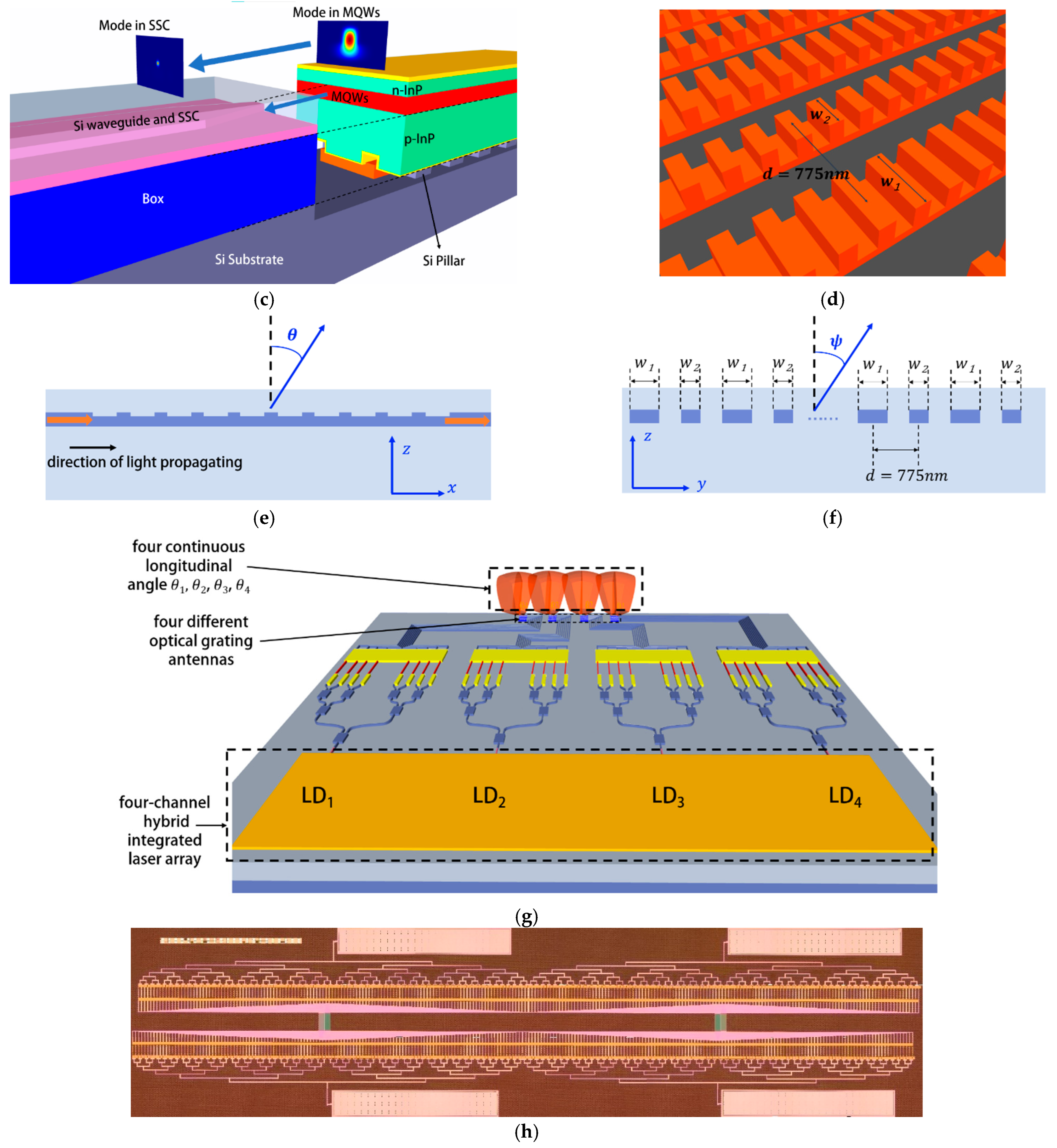
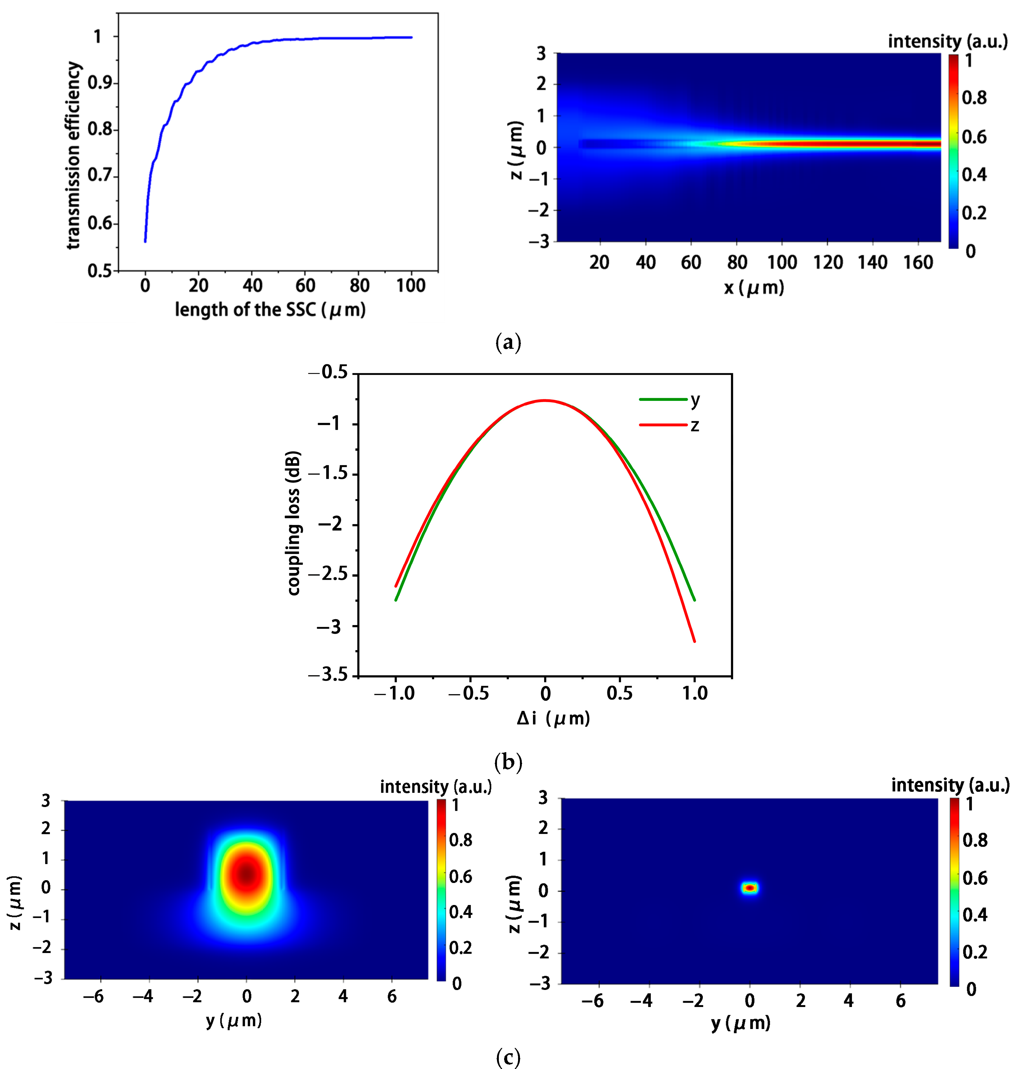
2.1. Semiconductor Laser and SSC

The optical mode is confined to the center of the active region by the waveguide of the single-mode ridge waveguide laser. An anti-tapered SSC is applied for matching the near-field pattern from the active III–V waveguide to the silicon waveguide.
The InP semiconductor laser design follows our previous approach [28]. The continuous tuning range of the tunable semiconductor laser is significantly improved by optimizing the length of the phase section using the gain–lever effect. It consists of four sections: a gain section, a phase section, a front mirror section, and a back mirror section. Both mirror sections contain a set of surface high-order gratings consisting of periodic slots. Each of these four sections corresponds to an independent electrode. By applying different current combinations to the multi-electrodes, quasi-continuous tuning range covering the C-band is achieved. The ridge waveguide, slots, and isolation trench of lasers are patterned with standard ultraviolet lithography on the epitaxial wafer, followed by Inductively Coupled Plasma Etch (ICP) to create deep etching for the ridge, slots, and shallow etching for the trench, while the trench separates the longer and shorter electrodes to enable independent electrical biasing. This laser could cover a 35 nm spectral range in the C-band (1530 nm to 1565 nm), as shown in Figure 2.
The anti-tapered input SSC taper width is 90 nm, tapering up to 450 nm via 150 µm length. The etching depth of the rib waveguide is 150 nm in a 220 nm silicon device layer. Calculating by Eigenmode Expansion (EME) solver, we configure a 2D simulation domain with localized mesh refinement in the central subwavelength region while implementing metal (PEC) boundary conditions. Thus, we can see that the coupling efficiency of this SSC can reach 99.5% when the length of the SSC is more than 60 microns, as shown in Figure 3a. With reference to the layout design rules, we specified the SSC length as 150 μm. Based on a previous work [29], we developed the fabrication process of the laser diode for hybrid integration. The recesses in the p-doped InP layer are fabricated to interconnect silicon pillars on the Si substrate, as shown in Figure 1b. The silicon pillars are etched from the silicon substrate, ensuring that their top surfaces remain coplanar with the substrate surface. By designing the thickness of the p-doped InP layer to match that of the Buried Oxide (BOX) layer, we achieve coplanar alignment of the Multiple Quantum Wells (MQWs) active layer, SSC, and Si waveguide layer in the vertical (Z-axis) direction. In the practical alignment process between the laser and SSC, we must consider the alignment tolerance. Therefore, we simulated the coupling loss variations under y-direction and z-direction misalignments to determine the 1 dB alignment tolerance. The 1 dB alignment tolerance is defined as the positional offset at which the coupling loss increases by 1 dB compared to the minimum loss. As shown in Figure 3b, calculating by Finite Difference Eigenmode (FDE) solver, the 1 dB alignment tolerance ranges from −0.7 µm to +0.7 µm in both y- and z-directions. Therefore, alignment within a 1.96 μm2 area ensures acceptable coupling loss. After thermal annealing for the alloys on the wafer, lithography and developing for patterned Au80Sn20 solder are implemented. Finally, the solder is lifted off according to the lithographic pattern. The thickness of the AuSn solder is 3 µm. The patterned solder provides an intimate connection and an efficient heat dissipation channel between the III–V component and the silicon substrate. Meanwhile, the patterned AuSn solder avoids contaminating the facets. The III–V laser array could be transferred to the SOI substrate by a flip–chip bonder (such as Finetech Fineplacer Lambda flip–chip bonder) via the 3 µm AuSn as solder. An efficient modal is transferred from the III–V waveguide to the silicon waveguide of OPA by the adiabatic anti-tapered SSC. Figure 3c shows the mode before and after entering the SSC.

2.2. Vertical Beam-Steering Angle θ

Figure 1e shows the cross-section view of an emitter. Figure 1f shows the cross-section view of the non-uniform width emitters. The grating structure along the waveguide diffracts the light off the chip following the grating Equation (1):
sin θ = Λ n e f f λ Λ
where θ represents the vertical steering angle in the cross-section plane, λ is the laser wavelength, Λ is the grating period, and n e f f is the effective refractive index of the mode propagating in the waveguide. As is described in Equation (1), θ depends on the laser wavelength, so a widely tunable laser is required to increase the vertical beam’s steering range. An external laser with a large tuning range is used usually, but the laser source should also be miniaturized, considering volume, stability, and cost. Single-chip semiconductor laser could also be used because of its volume and cost, but its tuning range is too small. The vertical steering angle has been limited by the tradeoff between the larger tuning range of the external laser and the lower volume, higher stability, and the lower cost of the single-chip semiconductor laser. To address this, we innovatively design a multi-lines OPA in a single chip. The illustration of a four-line OPA chip is shown in Figure 1g. According to Equation (1), θ also depends on the grating period and the effective refractive index besides the wavelength. Therefore, we can alter the vertical steering angle with different optical gratings when using the same tuning range laser. Each OPA possesses different output grating period and duty cycle, corresponding to multi same tuning range semiconductor lasers and multi continuous vertical beam steering range. This scheme allows several lasers to be fabricated from the same III–V epitaxial wafer and integrated on the OPAs chip at same time, multiplying the tuning efficiency several times, realizing the same vertical beam steering range as the external lasers but only with one-eighth wavelength tuning range of the external lasers, and the hybrid integration scheme also greatly reduces its preparation cost and volume, improving its compactness.

2.3. Horizontal Beam-Steering Angle ψ

Adjusting the optical phase in each channel via the phase shifters changes the wave front emitted from the arrayed antennas. For a given waveguide pitch d , the aliasing-free horizontal beam-steering angle ψ of the 0th-order beam can be determined by the location of ±1st-order grating lobes, and it can be approximated as [18]
ψ = a r c sin λ 2 d
The horizontal beam-steering angle ψ reaches ±90° when pitch is less than or equal to half the wavelength (the pitch is 775 nm when the wavelength is 1550 nm), as seen in Equation (2). When the width is uniform, the effective refractive index of the nearest waveguide is the same, so a half-wavelength pitch is difficult to achieve because of the strong evanescent coupling in a narrow pitch between the nearest emitter waveguides when the width is uniform.
Figure 4a shows the simulation of optical power distribution induced by the crosstalk from the evanescent coupling between the uniform-width waveguide arrays, calculated using the finite-difference time-domain (FDTD) method. We configured a 3D simulation domain with mesh refinement level 2, implementing perfectly matched layer (PML) boundary conditions. The width and the pitch were set to be 450 nm and 775 nm. The fundamental transverse electric (TE) mode with a wavelength of 1550 nm was incident on the main waveguide, that is, in the middle. As Figure 4a shows, the optical power from the main waveguide was significantly transferred to the nearest side waveguides, but it hardly transferred to the second-nearest waveguides.
The ratio of transferred power from the main waveguide to the side waveguide P 1 2 / P 1 (we can use it to represent the intensity of crosstalk) can be expressed as [30]
P 1 2 P 1 = 1 1 + Δ β 2 κ 2 sin 2 κ 2 L + Δ β 2 2
where Δ β represents the phase mismatch (or propagation constant difference) between the main waveguide and the side waveguide that is inversely proportional to the difference in waveguide widths, and κ represents the coupling strength (or coupling coefficient). From Equation (3), the maximum crosstalk is given by max [ P 1 2 / P 1 ] = 1 / [ 1 + β / 2 κ 2 ] when s i n κ 2 L + Δ β / 2 2 = ± 1 , and the crosstalk can be reduced by increasing Δ β or decreasing κ , which are functions of the waveguide width and pitch. At a fixed pitch of d = 775   n m = λ / 2 , it is necessary to obtain the appropriate main waveguide width w 1, side waveguide width w 2, and range of waveguide width difference Δ w .
We designed two non-uniform width nearest waveguides, w 1 and w 2, to change the effective refractive index by changing the width, resulting in a phase mismatch, thus suppressing the evanescent coupling between the nearest waveguides. To determine the proper waveguide widths, we calculated the crosstalk between two waveguides, spaced 775 nm apart, by using Finite Difference Eigenmode (FDE) solver, and configured a 2D simulation domain with localized mesh refinement in the central subwavelength region while implementing PML boundary conditions. To ensure the limitation of the optical field by the silicon waveguide and better mode transmission, the width of the silicon waveguide should not be less than 400 nm. As shown in Figure 4c, the number in each small cell represents the crosstalk between the main and side waveguides of different widths; the red zone along the diagonal line shows the largest crosstalk (≈−5 dB) that appears when w 1 = w 2. The farther the area from the diagonal, the wider the waveguide and the lower the crosstalk. However, this also implies that when the minimum waveguide width is 400 nm, the larger waveguide width becomes excessively large, resulting in an overly narrow gap between the main and side waveguides, which may give a load in the lithography process. To achieve a crosstalk of approximately −30 dB, after comprehensively considering the two conflicting constraints of a minimum waveguide width of 400 nm and the precision of the lithography process, we set the width difference Δ w = 50   n m . As shown in Figure 4a, the two blue green regions circled with white dashed lines represent Δ w = 50   n m , while the two data circled with red solid lines represent that when w 1 (or w 2) =450 nm and w 2 (or w 1) = 400 nm, the crosstalk is −31.78 dB and −29.7 dB, respectively. Thus, we determined that w 1 = 450 nm, w 2 = 400 and Δ w = 50 nm; in this case, the crosstalk is reduced by approximately −30 dB. Figure 4b shows the simulation of optical power distribution in this condition, in which the crosstalk from the evanescent coupling was suppressed effectively.

2.4. Far-Field Beamwidth of the Main Lobe Δ ψ

The width of the main lobe at the half-power level of the array radiation intensity represents the optical beam resolution Δ ψ that fits the following expression: [18]
Δ ψ = C λ N d sin ψ
where C is the constant, N is the number of the waveguide emitters, and ψ is the beam-steering angle. This expression shows that the beamwidth Δ ψ is inversely proportional to the size of arrayed antenna N d . It is necessary to have as large of an N as possible when the pitch stays the same in order to achieve a narrow beamwidth. Longer detection distance will reduce resolution accuracy, so high-resolution 3D sensing requires a very narrow beamwidth, especially in automotive applications, where beamwidth should be better than 0.4° for object identification at 50 m. We used FDTD to simulate the beamwidth of the far-field with different numbers of waveguide emitters and plotted them in the same coordinate system, as shown in Figure 5. We set the waveguide pitch to a half-wavelength of 775 nm and the number of the waveguide emitters from 128, 256, 512, and 1024 sequentially, and the beamwidth could be simulated to be 0.3876°, 0.2076°, 0.1163°, and 0.0581°, respectively, in accordance with the expression that beamwidth is inversely proportional to the size of arrayed antenna. This also proves that the scheme in which we chose the 128-channel emitter is compliant with the vehicle specification class where the beamwidth is less than 0.4° for object identification at 50 m.

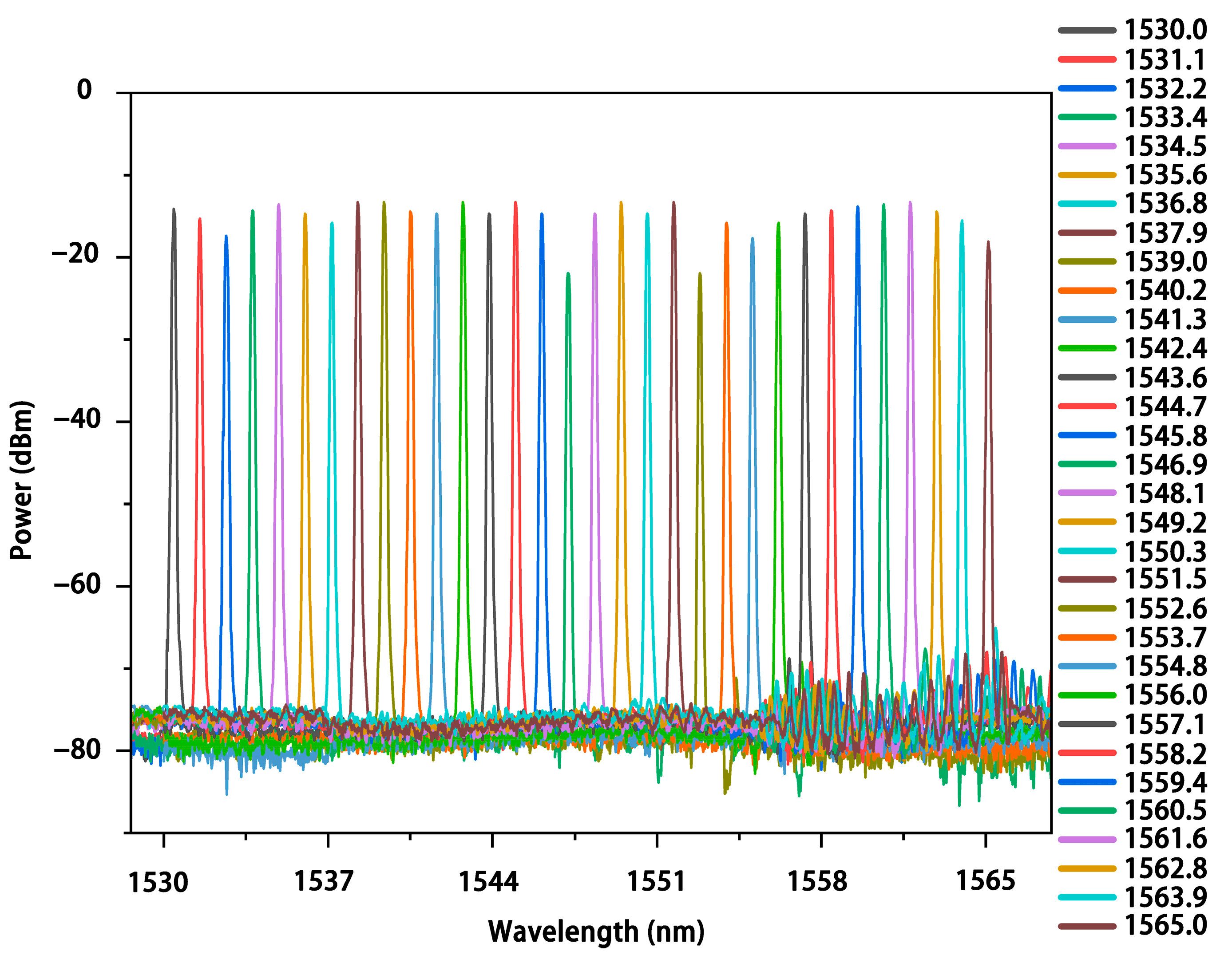
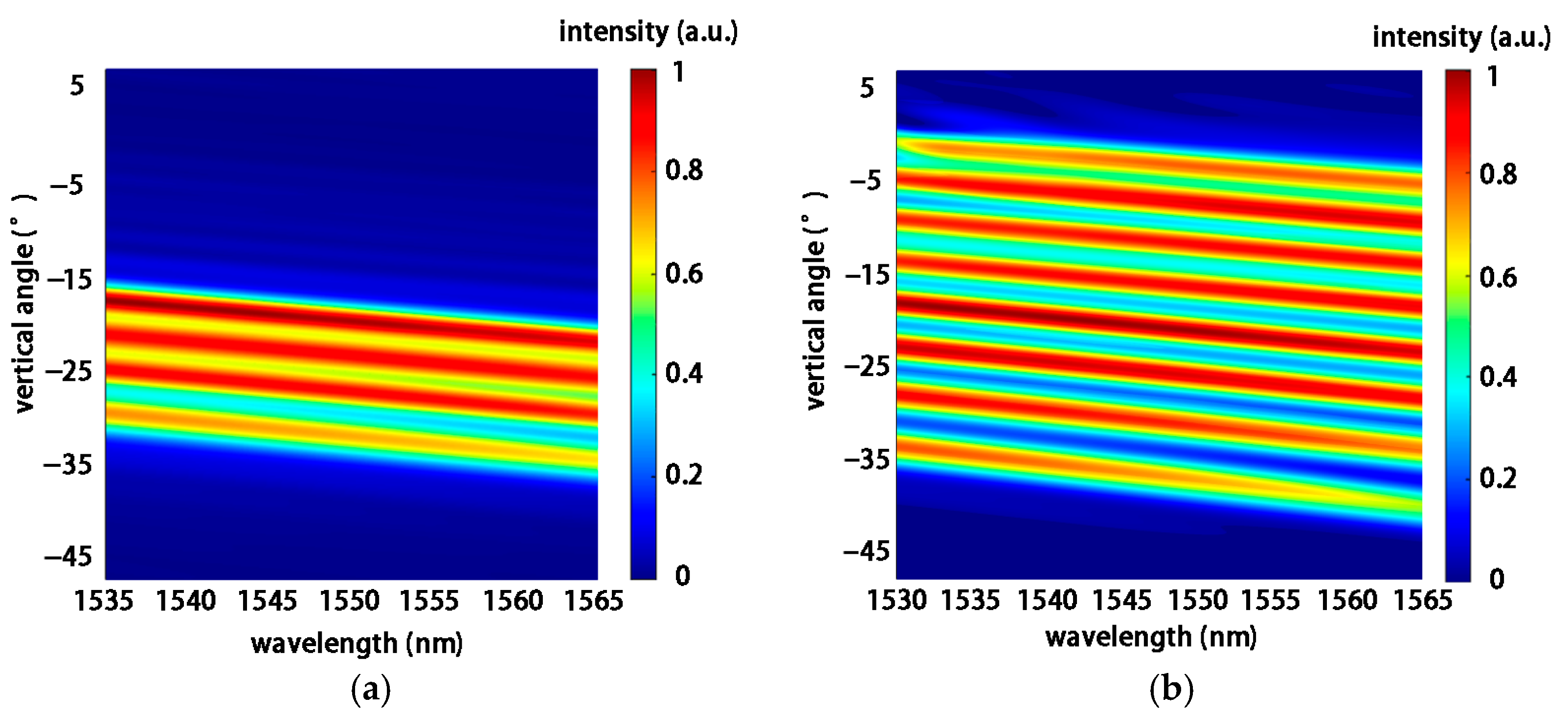
3. Simulation and Results

The optical grating antenna is designed on the Silicon-On-Insulator (SOI) structure with the top silicon being 220 nm in thickness, the BOX thickness is 2 μm, and the etching depth of the grating is 70 nm; it was designed using FDTD method. When using the four-line OPA in a single chip, in order to expand the vertical angle θ , to make four angles continuous, and to suppress the higher-order grating lobes, this paper uses Parameter Optimizations and Sweeps algorithm of the FDTD method; both grating period and duty cycle are variables instead of changing the period with a fixed duty cycle (the angles obtained in this way may not be the optimal solution). The duty cycle is set from 20% to 80%, every 5% is a step; the grating period is set from 400 nm to 650 nm, every 5 nm is a step; a total of 663 calculations and four optimal solutions are obtained, and the results are shown in Table 2a. The first optical grating antenna with a grating period of 475 nm and a duty cycle of 60% indicate that the beam steers from −29.6° to −34.6° in the θ direction when the wavelength tunes from 1535 nm to 1565 nm. The single OPA can scan 5.0° in the θ direction when tuning 30 nm wavelength. The second, third, and fourth optical grating antennas with the grating/duty cycles of 500 nm/30%, 510 nm/30%, and 500 nm/70% show that the beam steers from −29.6° to −34.6°, from −24.8°to −29.7°, and from −17.4° to −21.9° in the θ direction, respectively, and scan 4.9°, 4.6°, and 4.5° when tuning 30 nm wavelength, respectively. In the 30 nm tuning range of 1535 nm~1565 nm, the hybrid-integrated four-line OPA can get a scanning range of 17.2° in the θ direction, and the tuning efficiency is 0.572°/nm, much larger than indicated in past reports [3]. Although CMOS processes are highly mature at the scale of 500 nm, in our design, we still ensure vertical angular overlap for each grating antenna to enhance acceptable fabrication tolerance. The total overlap angle of 1.88° exceeds 10% of the total angular range, significantly enhancing acceptable fabrication tolerance. The simulation results of four-line OPA are shown in Figure 6a. Furthermore, in order to expand the four lines to eight lines, change the step size of the grating period to 1 nm to improve the accuracy of the algorithm, and finally obtain eight optimal solutions, the results of which are shown in Table 2b. The 35 nm tuning range in the entire C-band of 1530~1565 nm realizes a beam steering range of 39.6° in the θ direction, and the tuning efficiency is further improved to 1.13°/nm. The total overlap angle of 3.0° constitutes approximately 8% of the total angular range, which remains an acceptable fabrication tolerance. The simulation results of eight-line OPA are shown in Figure 6b.
The horizontal beam-steering angle ψ is also simulated by the FDTD method. We comparatively present the far-field distributions of two schemes’ waveguides: the pitch is 775 nm (uniform 450 nm waveguides, non-uniform waveguides with alternating 400 nm/450 nm widths) in Figure 7a–e. The phase differences of 0°, 90°, 150°, 173°, and 180° generate corresponding horizontal angles of ψ = 0°, 30°, 55°, 80°, and 90°, respectively. It is clear from the curve that the intensity of non-uniform width waveguide scheme is stronger than the uniform one at any angle ψ . At a phase difference of 180°, the far-field pattern exhibits symmetric distribution at ψ = ±90°. This symmetry arises because a 180° phase difference implies binary phase states (0° and 180°) across all grating elements. Although half-wavelength waveguide pitch theoretically enables ±90° horizontal beam steering, this symmetry significantly degrades directivity, reducing OPA usability at ψ = ±90°. However, simulations confirm that an 80° horizontal angle can be achieved at a 173° phase difference, as demonstrated in Figure 7d. Figure 7f shows the beam steering of non-uniform-width waveguide arrays when the phase shifts changes. It can be observed that this scheme enables a horizontal steering range of nearly ±90° in the ψ direction.
In the aforementioned simulations, beam steering was independently demonstrated across two dimensions. For practical deployment, lookup tables (LUTs) must be established to correlate laser drive currents with emission wavelengths and phase shifter bias currents with relative phase shifts. By applying calibrated currents to both components, precise wavelength and waveguide phase shifts can be achieved, thereby enabling two-dimensional beam steering. For instance, driving LD1 with 1565 nm emission current while maintaining 150° phase difference across phase shifters produces output beams at ( ψ , θ ) = (−55°, −40.3°) by first grating.

4. Perspectives and Discussion

We have fabricated a hybrid-integrated OPA prototype based on passive alignment technology, as seen in Figure 1h. The OPA and photonic passive devices are fabricated using the CompoundTek 200 mm mature Si Photonics process. The passive alignment hybrid integration based on an interconnect structure is compatible with commercial CMOS foundries. The eight-inch silicon wafer used in the fabrication of the OPA chip is fabricated together with other devices such as the Mach–Zehnder modulator at the same batch, so in order to make better use of the area on the silicon wafer, the layout of the four OPAs designed and fabricated in the first time has some differences with the illustration, as seen in Figure 1g, but the structure of a single OPA is the same. There are also four arrays of OPA in our fabricated chip, where each OPA has 128 gratings, the spacing of each grating waveguide is a half wavelength of 775 nm, and the waveguide widths are alternately 450 nm and 400 nm. In the future, we will extend this research by completing experimental characterization and testing of the proposed OPA chip.

5. Conclusions

In this paper, we propose a hybrid-integrated III–V-silicon OPA based on passive alignment flip–chip bonding technology and provide new solutions for LiDAR, one with smaller volume, higher stability, and lower cost. We designed a half-wavelength waveguide pitch and a non-uniform waveguide width grating antenna to achieve a low crosstalk from the nearest waveguides and a nearly ±90° horizontal beam steering range. We also propose a scheme that allows several lasers to be fabricated from the same III–V epitaxial wafer and integrated on the OPAs chip at same time to multiply the tuning efficiency several times. Based on the simulations, we simultaneously achieved a 39.6° vertical beam steering range and a high tuning efficiency of 1.13°/nm. We also achieved an angular overlap ratio of approximately 10%, thus enhancing acceptable fabrication tolerance of the grating antenna. Ultimately, the far-field beamwidth with different numbers of the waveguide emitters from 128, 256, 512, and 1024 has been discussed. Using simulation, we designed a 128-channel emitter with a far-field beamwidth of 0.3876°, which can be less than 0.4° for object identification at 50 m.

Author Contributions

Conceptualization, S.Z. and M.W.; methodology, S.Z.; software, S.Z., Z.Y. and J.S.; validation, S.Z.; formal analysis, S.Z.; investigation, S.Z.; resources, W.Z.; data curation, S.Z.; writing—original draft preparation, S.Z.; writing—review and editing, S.Z., M.W. and J.C.; visualization, S.Z., Z.Y. and J.S.; supervision, M.W. and W.Z.; project administration, W.Z.; funding acquisition, W.Z. All authors have read and agreed to the published version of the manuscript.

Funding

This research was funded by the National Key Research and Development Program of China (2021YFB2801400), the National Natural Science Foundation of China (62205328), and the Beijing Nova Program (20230484332).

Institutional Review Board Statement

Not applicable.

Informed Consent Statement

Not applicable.

Data Availability Statement

The data presented in this study are available on reasonable request from the corresponding author.

Acknowledgments

We sincerely appreciate the contributions of every author of this article.

Conflicts of Interest

The authors declare no conflicts of interest.

References

  1. Zhang, Y.; Ling, Y.-C.; Zhang, K.; Gentry, C.; Sadighi, D.; Whaley, G.; Colosimo, J.; Suni, P.; Yoo, S.J.B. Sub-wavelength-pitch Silicon-Photonic Optical Phased Array for Large Field-of-Regard Coherent Optical Beam Steering. In Proceedings of the 44th Annual European Conference on Optical Communications (ECOC), Rome, Italy, 23–27 September 2018. [Google Scholar]
  2. Im, C.S.; Bhandari, B.; Lee, K.P.; Kim, S.M.; Oh, M.C.; Lee, S.S. Silicon nitride optical phased array based on a grating antenna enabling wavelength-tuned beam steering. Opt. Express 2020, 28, 3270–3279. [Google Scholar] [CrossRef] [PubMed]
  3. Sun, X.C.; Zhang, L.X.; Zhang, Q.H.; Zhang, W.F. Si Photonics for Practical LiDAR Solutions. Appl. Sci. 2019, 9, 4225. [Google Scholar] [CrossRef]
  4. Shuai, Y.Q.; Zhou, Z.P.; Su, H. Toward Practical Optical Phased Arrays through Grating Antenna Engineering. Photonics 2023, 10, 520. [Google Scholar] [CrossRef]
  5. Vuthea, V.; Toshiyoshi, H. A Design of Risley Scanner for LiDAR Applications. In Proceedings of the International Conference on Optical MEMS and Nanophotonics (OMN), Lausanne, Switzerland, 29 July–2 August 2018; pp. 135–136. [Google Scholar]
  6. Kamerman, G.W.; Turner, M.D.; Wang, D.; Bai, Y.; Stainsby, A.; Koppal, S.; Strassle, S.; Xie, H. A compact 3D lidar based on an electrothermal two-axis MEMS scanner for small UAV. In Proceedings of the Laser Radar Technology and Applications XXIII, Orlando, FL, USA, 17–18 April 2018. [Google Scholar]
  7. Kasturi, A.; Milanovic, V.; Atwood, B.H.; Yang, J. UAV-Borne LiDAR with MEMS Mirror-Based Scanning Capability. In Proceedings of the Conference on Laser Radar Technology and Applications XXI, Baltimore, MD, USA, 19–20 April 2016. [Google Scholar]
  8. Lemmetti, J.; Sorri, N.; Kallioniemi, I.; Melanen, P.; Uusimaa, P. Long-range all-solid-state flash LiDAR sensor for autonomous driving. In Proceedings of the Conference on High-Power Diode Laser Technology XIX, Electronic Network, 6–11 March 2021. [Google Scholar]
  9. Zhang, C.; Lindner, S.; Antolovic, I.M.; Pavia, J.M.; Wolf, M.; Charbon, E. A 30-frames/s, 252 × 144 SPAD Flash LiDAR with 1728 Dual-Clock 48.8-ps TDCs, and Pixel-Wise Integrated Histogramming. IEEE J. Solid-State Circuit 2019, 54, 1137–1151. [Google Scholar] [CrossRef]
  10. Jo, S.; Kong, H.J.; Bang, H.; Kim, J.W.; Kim, J.; Choi, S. High resolution three-dimensional flash LIDAR system using a polarization modulating Pockels cell and a micro-polarizer CCD camera. Opt. Express 2016, 24, A1580–A1585. [Google Scholar] [CrossRef]
  11. Poulton, C.V.; Yaacobi, A.; Cole, D.B.; Byrd, M.J.; Raval, M.; Vermeulen, D.; Watts, M.R. Coherent solid-state LIDAR with silicon photonic optical phased arrays. Opt. Lett. 2017, 42, 4091–4094. [Google Scholar] [CrossRef]
  12. Nakamura, K.; Narumi, K.; Kikuchi, K.; Inada, Y.; He, S.; Vivien, L. Liquid-crystal tunable optical phased array for LiDAR applications. In Proceedings of the Smart Photonic and Optoelectronic Integrated Circuits XXIII, Online, 6–11 March 2021. [Google Scholar]
  13. Yoon, J.; Yoon, H.; Kim, J.Y.; Kim, J.; Kang, G.M.; Kwon, N.H.; Kurt, H.; Park, H.H. Demonstration of high-accuracy 3D imaging using a Si optical phased array with a tunable radiator. Opt. Express 2023, 31, 9935–9944. [Google Scholar] [CrossRef]
  14. Zhao, S.; Lian, D.X.; Chen, J.Y.; Dai, D.X.; Shi, Y.C. Polarization multiplexing silicon photonic optical phased array with a wide scanning range. Opt. Lett. 2023, 48, 6092–6095. [Google Scholar] [CrossRef]
  15. Desantis, D.M.; Mazur, B.M.; Notaros, M.; Notaros, J. Multi-beam solid-state LiDAR using star-coupler-based optical phased arrays. Opt. Express 2024, 32, 36656–36673. [Google Scholar] [CrossRef]
  16. Chen, R.X.; Shu, H.W.; Shen, B.T.; Chang, L.; Xie, W.Q.; Liao, W.C.; Tao, Z.H.; Bowers, J.E.; Wang, X.J. Breaking the temporal and frequency congestion of LiDAR by parallel chaos. Nat. Photonics 2023, 17, 306–314. [Google Scholar] [CrossRef]
  17. Doylend, J.K.; Heck, M.J.R.; Bovington, J.T.; Peters, J.D.; Coldren, L.A.; Bowers, J.E. Two-dimensional free-space beam steering with an optical phased array on silicon-on-insulator. Opt. Express 2011, 19, 21595–21604. [Google Scholar] [CrossRef] [PubMed]
  18. Van Acoleyen, K.; Bogaerts, W.; Jágerská, J.; Le Thomas, N.; Houdré, R.; Baets, R. Off-chip beam steering with a one-dimensional optical phased array on silicon-on-insulator. Opt. Lett. 2009, 34, 1477–1479. [Google Scholar] [CrossRef]
  19. Hulme, J.C.; Doylend, J.K.; Heck, M.J.R.; Peters, J.D.; Davenport, M.L.; Bovington, J.T.; Coldren, L.A.; Bowers, J.E. Fully integrated hybrid silicon two dimensional beam scanner. Opt. Express 2015, 23, 5861–5874. [Google Scholar] [CrossRef] [PubMed]
  20. Misugi, Y.; Okayama, H.; Kita, T. Compact and Low Power-Consumption Solid-State Two-Dimensional Beam Scanner Integrating a Passive Optical Phased Array and Hybrid Wavelength-Tunable Laser Diode. J. Light. Technol. 2023, 41, 3505–3512. [Google Scholar] [CrossRef]
  21. Liang, D.; Li, W.L.; Wang, X.B.; Zhao, X.; Guo, Z.C.; Han, X.E.; Chen, J.Y.; Dai, D.X.; Shi, Y.C. Grating lobe-free silicon optical phased array with periodically bending modulation of dense antennas. Opt. Express 2023, 31, 11423–11430. [Google Scholar] [CrossRef]
  22. Chen, J.Y.; Li, W.L.; Lian, D.X.; Zhao, S.; Dai, D.X.; Shi, Y.C. Coaxial transceiving LiDAR based on a silicon photonic optical phased array. Opt. Lett. 2024, 49, 3424–3427. [Google Scholar] [CrossRef]
  23. Chung, S.; Abediasl, H.; Hashemi, H. A Monolithically Integrated Large-Scale Optical Phased Array in Silicon-on-Insulator CMOS. IEEE J. Solid-State Circuit 2018, 53, 275–296. [Google Scholar] [CrossRef]
  24. Kwong, D.; Hosseini, A.; Zhang, Y.; Chen, R.T. 1 × 12 Unequally spaced waveguide array for actively tuned optical phased array on a silicon nanomembrane. Appl. Phys. Lett. 2011, 99, 051104. [Google Scholar] [CrossRef]
  25. Hutchison, D.N.; Sun, J.; Doylend, J.K.; Kumar, R.; Heck, J.; Kim, W.; Phare, C.T.; Feshali, A.; Rong, H.S. High-resolution aliasing-free optical beam steering. Optica 2016, 3, 887–890. [Google Scholar] [CrossRef]
  26. Phare, C.T.; Shin, M.C.; Sharma, J.; Ahasan, S.; Krishnaswamy, H.; Lipson, M. Silicon Optical Phased Array with Grating Lobe-Free Beam Formation over 180 Degree Field of View. In Proceedings of the Conference on Lasers and Electro-Optics (CLEO), San Jose, CA, USA, 13–18 May 2018. [Google Scholar]
  27. Wang, M.; Dong, F.; Meng, R.; Ma, P.; Liu, J.; Wang, H.; Wang, X.; Zheng, W. Eight-channel hybrid-integrated laser array with 100 GHz channel spacing. Electron. Lett. 2020, 56, 1032–1093. [Google Scholar] [CrossRef]
  28. Du, F.; Xu, Y.; Li, J.; Wang, H.; Zheng, W. Quasi-continuous tunable semiconductor laser based on the gain-lever effect with full C-band coverage fabricated by standard lithography. Appl. Opt. 2022, 61, 7343–7348. [Google Scholar] [CrossRef]
  29. Wang, M.J.; Liu, W.Z.; Xu, Y.B.; Fu, T.; Chen, J.X.; Zheng, W.H. Single-chip hybrid integrated silicon photonics transmitter based on passive alignment. Opt. Lett. 2022, 47, 1709–1712. [Google Scholar] [CrossRef] [PubMed]
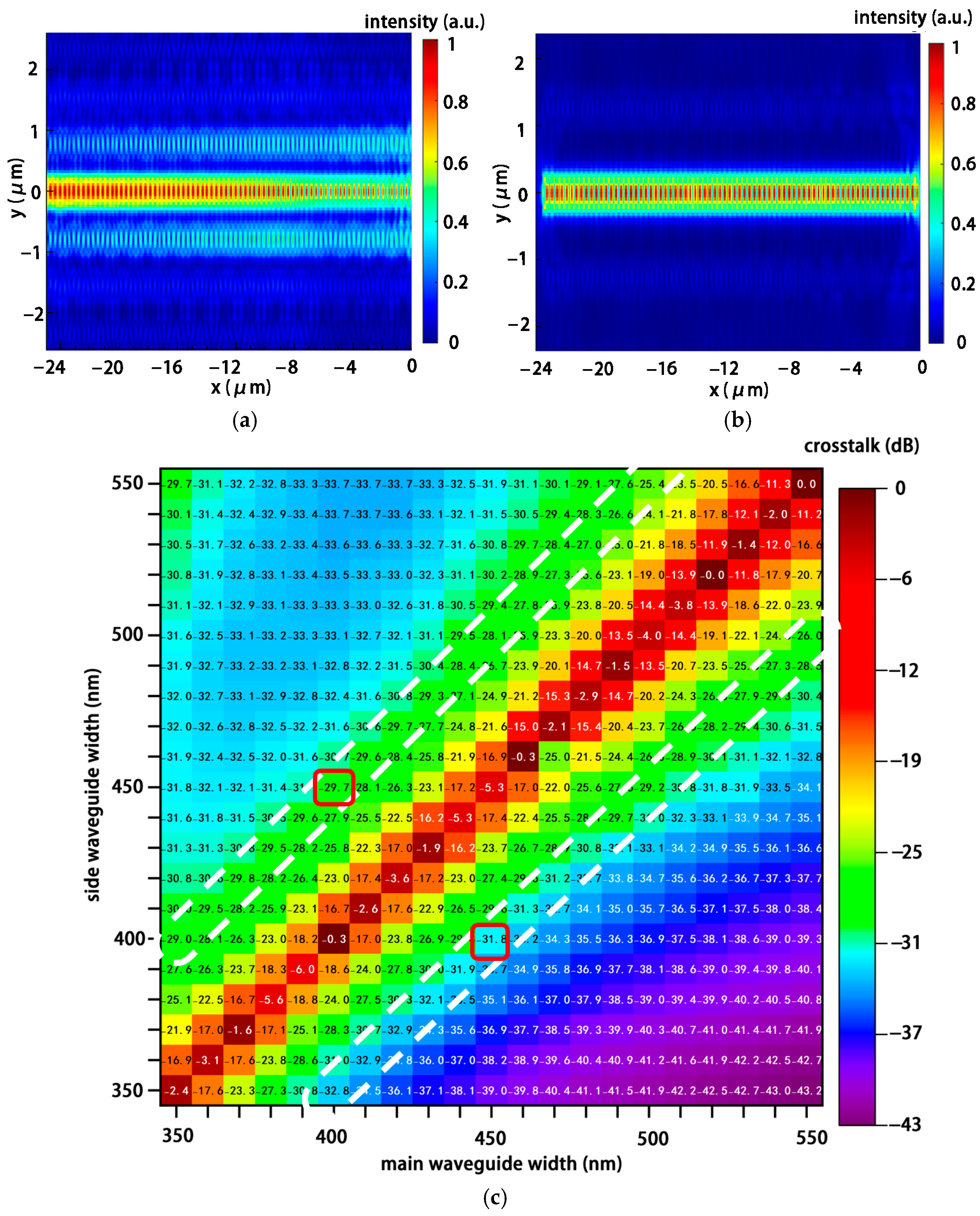
  30. Song, W.W.; Gatdula, R.; Abbaslou, S.; Lu, M.; Stein, A.; Lai, W.Y.C.; Provine, J.; Pease, R.F.W.; Christodoulides, D.N.; Jiang, W. High-density waveguide superlattices with low crosstalk. Nat. Commun. 2015, 6, 7027. [Google Scholar] [CrossRef]
Figure 1. (a) Top view of an OPA; (b) cross-section view of the Spot Size Converter (SSC); (c) hybrid integration of laser and OPA chip via the SSC; (d) non-uniform width emitters; (e) cross-section view of an emitter; (f) cross-section view of the non-uniform width emitters; (g) illustration of a four-line OPA chip; (h) micrograph of the hybrid-integrated OPA chip prototype.
Photonics 12 00699 g001aPhotonics 12 00699 g001b
Figure 2. Spectrum of a C-band tunable laser.
Photonics 12 00699 g002
Figure 3. (a) Relationship between the efficiency and length of SSC; (b) alignment tolerance of laser and SSC butt-coupling on xy plane; (c) mode before and after entering the SSC.
Photonics 12 00699 g003
Figure 4. (a) Simulation of optical power distribution between the uniform-width waveguide arrays; (b) simulation of optical power distribution between the non-uniform-width waveguide arrays; (c) simulation of crosstalk between the nearest waveguides of different widths.
Photonics 12 00699 g004
Figure 5. Far-field beamwidth at different number of the waveguide emitters.
Photonics 12 00699 g005
Figure 6. (a) Simulation of far-field distributions of the four-line OPA in the θ direction; (b) simulation of far-field distributions of the eight-line OPA in the θ direction.
Photonics 12 00699 g006
Figure 7. (ae) Far-field distributions of uniform-width waveguide arrays when the phase shifts are 0°, 90°, 150°, 173°, and 180°; (f) beam steering of non-uniform-width waveguide arrays when the phase shifts change.
Photonics 12 00699 g007
Table 1. Comparative analysis between state-of-the-art OPAs and the proposed scheme.
TimeWhether Laser Is Integrated ψ θ Tuning EfficiencyWavelengthsApproachLiterature
2023No60°24.8°0.31°/nm1520 nm~1600 nmPolarization switch[14]
2024No40°0.133°/nm1540 nm~1600 nmCoaxial transceiver[22]
2023Yes44.2°13.7°0.137°/nm1500 nm~1600 nmExternal cavity[20]
2023No120°--1550 nmBent waveguide arrays[21]
2025Yes180°39.6°1.13°/nm1530 nm~1565 nmMulti-lines lasers and antennasThis work
Table 2. (a) Simulation of the four-line OPA in the θ direction; (b) simulation of the eight-line OPA in the θ direction.
Period
Duty Cycle
475 nm/
60%
500 nm/
30%
510 nm/
30%
500 nm/
70%
θ   ( 1535   nm ) −29.6°−24.8°−21.1°−17.4°
θ   ( 1565   nm ) −34.6°−29.7°−25.7°−21.9°
Single range5.0°4.9°4.6°4.5°
Intensity0.750.860.850.97
Total range17.2°
Total overlap Angle1.88°
Tuning efficiency0.57°/nm
(a)
Period/
Duty cycle
476 nm/
30%
471 nm/
70%
483 nm/
70%
495 nm/
70%
529 nm/
30%
527 nm/
60%
541 nm/
60%
562 nm/
50%
θ   ( 1530 nm ) −33.7°−28.0°−22.9°−18.1°−13.6°−9.1°−4.6°−0.7°
θ   ( 1565   nm ) −40.3°−34.0°−28.5°−23.4°−18.6°−13.9°−9.4°−5.2°
Single range6.6°6.0°5.6°5.3°5.0°4.8°4.8°4.5°
intensity0.750.800.850.890.800.760.790.71
Total range39.6°
Total overlap Angle3.0°
Tuning efficiency1.13°/nm
(b)
Disclaimer/Publisher’s Note: The statements, opinions and data contained in all publications are solely those of the individual author(s) and contributor(s) and not of MDPI and/or the editor(s). MDPI and/or the editor(s) disclaim responsibility for any injury to people or property resulting from any ideas, methods, instructions or products referred to in the content.

