Article

Highly Efficient Digitized Quasi-3D Photolithography Based on a Modified Golomb Coding via DMD Laser Direct Writing

School of Science, Zhejiang University of Science and Technology, Hangzhou 310023, China
*
Author to whom correspondence should be addressed.
Photonics 2025, 12(6), 587; https://doi.org/10.3390/photonics12060587
Submission received: 25 April 2025 / Revised: 18 May 2025 / Accepted: 23 May 2025 / Published: 9 June 2025

Abstract

Three-dimensional (3D) photolithography has found wide applications in microelectronics, optoelectronics, biomedicine, etc. Traditionally, it requires repetitive exposure and developing cycles. Meanwhile, a laser direct writing (LDW) system with a digital micromirror device (DMD) enables high-speed maskless lithography with programmable doses. In this paper, we propose a quasi-3D digitized photolithography via LDW with a DMD to remove multiple developing cycles from the process. This approach quantizes the dose of the 3D geometry and stores it in a grayscale image. And the entire dose distribution can be formed by overlapping the exposures with sliced binary dose maps from the above grayscale dose map. In the image slicing algorithm, a modified Golomb coding is introduced to make full use of the highest available exposure intensity. Both 1D multi-step patterns and diffractive optical devices (DOEs) have been fabricated to verify its feasibility. This type of digitized quasi-3D photolithography can be applied to fabricating DOEs, microlens arrays (MLAs), micro-refractive optical elements (μROEs), etc., and 3D molds for micro-embossing/nano-imprinting.

1. Introduction

Optical devices in modern society require a compact size and an inexpensive cost, yet without compromising their performance [1]. In the face of miniaturizing 3D optical devices, such as DOEs, microlens arrays (MLAs) [2], micro-refractive optical elements (μROEs) [3], etc., not only is a high transverse accuracy required but also a high depth accuracy is a must. And various photolithography technologies, such as electron beam lithography, direct writing lithography, two-photon/multi-photon lithography, laser 3D printing, etc. [4,5,6,7,8,9,10,11,12,13,14,15], have been developed for patterning 3D micro/nanostructures. Electron beam lithography and two-photon/multi-photon lithography can pattern complex 3D structures, but the patterning speed is relatively low. Laser 3D printing, such as laser sintering, also has a strong ability to create 3D structures down to several µm, but it usually requires additional heating and cleaning processes. On the other hand, direct writing lithography using a DMD has attracted increasing attention due to its high patterning speed, low cost, and high flexibility [14,15,16]. Consequently, various modifications have been made to DMD-based LDW for realizing 3D patterns [15,16,17,18,19,20]. Some split the exposure dose equally but increase the entire exposure time; others are assisted by additional components or by increasing the bit depth of the DMD (12-bit), which increases the complexity of the LDW system and/or its cost. In order to reduce the exposure time and still pattern using conventional (8-bit or less) DMD-based LDW, we propose digitized quasi-3D photolithography. It initially quantizes the required dose for the 3D pattern at each location and stores it into a grayscale image. Then, the grayscale dose map is further sliced into several binary images through bit plane slicing, storing 2D dose maps. Next, the overall dose is formed by overlapping the exposure with these sliced binary images. Finally, a quasi-3D pattern can be generated afterwards through one development step. This digitized photolithography approach can significantly reduce the exposure times (e.g., 256 dose levels with just eight exposures) without other forms of assistance.
In image slicing algorithms, direct binary coding is very convenient for the proposed digitized photolithography. However, such binary coding requires the dose to be distributed with an exponential power of 2, which may not be always achievable for LDW facilities, especially in terms of the maximum exposure intensity available. In order to make full use of the available exposure intensities of an LDW system, a modified Golomb coding is introduced during the image slicing step. The Golomb coding (GC) was originally a lossless data compression method proposed by S. Golomb [21]. With a modified GC, the maximum exposure intensity/dose is fully utilized, and it is suitable for different types of LDW with various dynamic exposure dose ranges. We name this type of quasi-3D photolithography using the modified GC approach the “GC-approach” for simplicity.
In this paper, we also experimentally compared the performance of the GC-approach and an “equal-dose scheme”, i.e., using an equal exposure dose for each exposure in fabricating 1D multi-step patterns. Apart from this, DOEs with 2D multi-step microstructures were demonstrated via the GC-approach.

2. The Background of Digitized Quasi-3D Photolithography

The developed depth of a positive photoresist is a logarithmic function of the exposure dose [18,19]:
d x , y = γ D l n E ( x , y ) E t h
Here, d(x, y) and E(x, y) are the depth and the exposure dose at (x, y), respectively. Meanwhile, D is the maximum depth corresponding to the maximum exposure dose E m a x , and E t h is the threshold dose for the photoresist to react. And γ is the contrast (inversely proportional to the absorption coefficient α of the resist), defined as the linear slope.
γ = 1 l n E m a x E t h 1 α
From Equations (1) and (2), we can control the depth at every position by setting an appropriate exposure dose when Eth and γD are experimentally determined. Inversely, we can derive the required exposure dose E(x, y) for each depth d(x, y) as shown below:
E x , y = E t h e d x , y γ D
For our LDW system (iGrapher UV200; throughput: 1100 mm2/min; compatible with an 8-inch wafer; provided by SVG Optronics, Co., Ltd., Suzhou, China), the irradiance/exposure intensity of the UV laser source is controlled by the operating current. The exposure dose with the current can be experimentally determined as demonstrated in Figure 1. Therefore, we can control the developed depth of the photoresist at each location using the desired dosage with the appropriate current.
In our proposed approach, the desired dose information is digitized and stored in one grayscale image. This digital image is sliced further into several binary images, which can be used to set the required exposure currents and expose the photoresist with an overlap. Finally, a 3D photoresist pattern can easily be created after one developing step.

3. The Scheme of Quasi-3D Photolithography

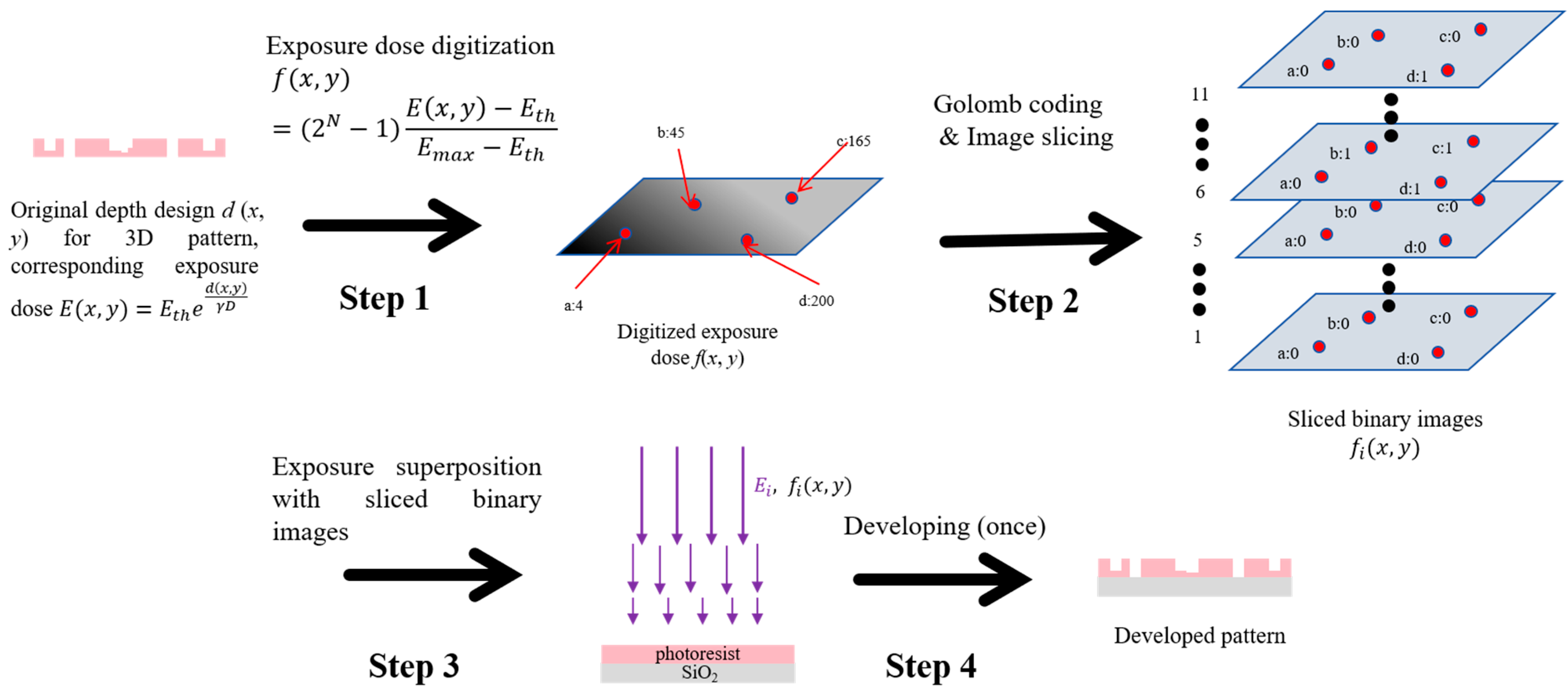
3.1. General Steps of Quasi-3D Photolithography

Based on the above background, the general steps of digitized quasi-3D photolithography are proposed as follows, and as shown in Figure 2.
Step 1: Estimate the required exposure dose E(x, y) from the designed depth d(x, y) via Equation (3). And the dose distribution E(x, y) is further digitized into a 2D grayscale image f(x, y); e.g., assuming an 8-bit grayscale image is used to store the relative distribution of the exposure dose, then a gray level of 255 represents the maximum exposure dose Emax, and a gray level of 0 represents the threshold exposure dose Eth. In general, for an N-bit grayscale image, the exposure dose E(x, y) is digitized as
f ( x , y ) = ( 2 N 1 ) E x , y E t h E m a x E t h
And from each digitized gray level f(x, y), the corresponding exposure dose E(x, y) can be decoded as
E x , y = f x , y 2 N 1 E max E th + E t h
Since digitization of the exposure dose is currently not suitable for hollow 3D structures, we label our scheme as quasi-3D photolithography, similar to grayscale lithography. But our approach is much faster using the LDW system (without additional physical masks).
Step 2: Slice the above grayscale image f(x, y) into M binary images using a modified Golomb coding. Through this image slicing process, the overall dose information is divided and stored in each binary image. If f i ( x , y ) denotes the intensity (1 or 0) of the i-th sliced binary image, the original grayscale image f(x, y) can be expressed as
f x , y = i M c i f i ( x , y )
ci here is the coefficient of the i-th sliced binary image, determined using the image slicing algorithm.
A slicing coefficient with an exponential power of 2 (i.e., c i = 2 i ) is simplest for image slicing. Practically, the available dose distribution may not always meet this requirement. In order to make full use of exposure intensities with an arbitrary distribution, the Golomb coding is introduced here.
Before coding, the range of the dynamic exposure dose for the LDW system is digitized as the maximum image slicing coefficient m at first. Using Equation (4), m is determined by the ratio between the maximum output exposure dose and the minimum, taking away the threshold dose:
m = E m a x E t h E m i n E t h = I m a x I t h I m i n I t h ( 2 N 1 )
Emax (≤Emax) here is the maximum exposure dose from a single exposure. Meanwhile, Emin (>Eth) is the minimum exposure dose for developing the shallowest depth. The value of m can be an arbitrary integer number, making full use of the available maximum intensity. If the exposure time is kept constant, the ratio can also be expressed as the ratio of the differences in intensity, as shown in Equation (7). Ith here is the threshold exposure intensity, related to the threshold exposure dose Eth.
In the general Golomb coding, there are two sections of binary code. The first section (higher bits) relates to the quotient q of the original value n and the parameter m, and the second one (lower bits) is the binary code of the remainder r between n and m (i.e., n = qm + r). In our scheme, the first section of the GC relates to the overlapping exposure with the maximum dose Emax, and the second one relates to that for a dose below Emax.
The first section of the proposed Golomb code here is a unary code of the rounded-down quotient q(x, y) between the gray level of f(x, y) and the parameter m:
q ( x , y ) = f ( x , y ) / m
f(x, y) here is the digitized exposure dose required for the maximum depth in the 3D design, as shown in Step 1. And q(x, y) indicates the number of exposures with the maximum exposure dose Emax.
Since the length of the code of the first section in the original Golomb code varies for different values, this is not suitable for image slicing. Consequently, the code length qmax for the first section is fixed here for all positions as the rounded-down quotient of the maximum gray level in the grayscale image f(x, y) and the parameter m:
q m a x = f ( x , y ) m a x / m
f ( x , y ) m a x is the maximum gray level in the grayscale image design f(x, y), corresponding to the exposure dose required for the maximum depth in the 3D design. Generally, there is qmaxq(x, y) of 0 s following q(x, y) of 1 s in the first section of the Golomb code.
Meanwhile, for the second section of the proposed GC, the code length k is determined by the rounded-up logarithm of m to the base of 2:
k = l o g 2 m
It is also the maximum number of exposures with an exposure dose below Emax.
We can still apply the Golomb coding rules for the second section as follows:
r x , y = f x , y q x , y m = f x , y   m o d   m
r x , y = k   b i t   b i n a r y   n u m b e r   o f   r ( x , y )
Here, r(x, y), the remainder of f(x, y) divided by m, represents the rest of the dose needed for exposure. And r’(x, y), the binary number of r(x, y), the second section of the Golomb code, describes the exposure scheme besides that with the dose Emax.
To sum up, the above two sections of code are concatenated pixel by pixel and stored in q max   +   k -sliced binary images as follows:
f i ( x , y ) = g i , 1 , 1 g i , 1 , T g i , S , 1 g i , S , T g i , x , y = 0,1 ; i [ 1 , q m a x + k ]
f i ( x , y ) is the sliced images storing the complete Golomb codes. Each sliced image f i ( x , y ) has the same pixel size as that in the original grayscale image design f(x, y) (e.g., S × T in Equation (13)). And gi,x,y represents the binary Golomb code for the i-th sliced image at coordinate (x, y). Correspondingly, the image slicing coefficient c i is 2 i for i = 1 ,   2 ,   ,   k (images with lower slicing) and m for i = k + 1 , k + 2 ,   ,   k + q max (images with higher slicing).
Substituting Equation (6) into Equation (5), the total exposure dose E(x, y) can also be expressed as
E x , y = i M c i f i ( x , y ) 2 N 1 E m a x E t h + E t h
Step 3: Expose the photoresist with an overlap with the sliced binary images f i ( x , y ) from Step 2 via DMD-based LDW. Assume the total exposure dose E(x, y) is the sum of all exposure doses at (x, y) as follows:
E x , y = i M E i f i x , y + E t h
Here, the threshold exposure dose Eth is listed separately to make Equation (15) comparable to Equation (14). And in order to make Equation (15) feasible, additional exposure with the uniform exposure dose Eth for the entire sample is needed beyond the exposures related to the sliced images. Comparing Equations (14) and (15), the single exposure dose Ei related to the i-th sliced image is derived as
E i = c i 2 N 1 E m a x E t h
When all of the exposure superpositions are conducted using the sliced image f i ( x , y ) and the corresponding dose Ei, as well as the uniform dose Eth, the overall dose meets the distribution in Equation (3).
Step 4: Develop the exposed sample once. Then, we can obtain a photoresist pattern with the desired 3D geometry according to Equation (1).
To sum up, the depth information of the 3D pattern’s design is initially converted into the required exposure dose distribution and further digitized into a grayscale image. Then, the overall exposure dose is reached by overlapping the exposures with the sliced binary images from the above depth-included grayscale image via the Golomb coding. Finally, the 3D pattern is formed after a single development step. Since the proposed digitized photolithography method separates the overlapping exposure and development, it is more efficient and more accurate than the traditional layer-by-layer photolithography in binary optics [22].

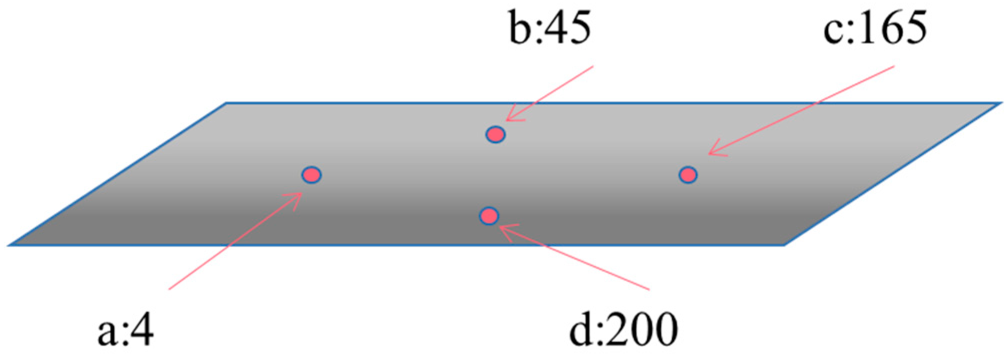
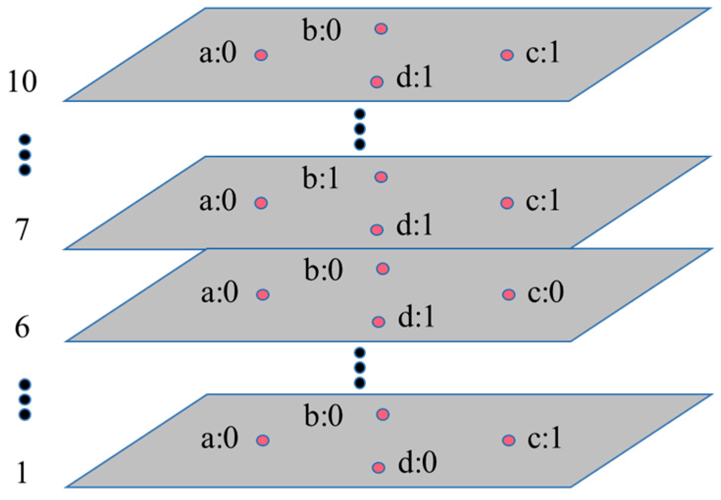
3.2. Numerical Illustration of Image Slicing with the Golomb Coding

A specific illustration is given here to demonstrate image slicing with the Golomb coding.
To begin with, we determine the maximum image slicing coefficient m corresponding to the dynamic exposure dose range of the photolithography facility, as shown in Equation (7); e.g., we assume m is measured as 41, and the digitized grayscale image derived in Equation (4) is demonstrated in Figure 3. For illustration, the gray levels of points a, b, c, and d in Figure 2 are 4, 45, 165, and 200, respectively.
Then, we encode the above grayscale image using the modified Golomb coding as proposed in Step 2 in Section 3.1. The Golomb code corresponding to points a–d is listed in Table 1.
Thirdly, binary images can be achieved through bit plane slicing (as shown in Figure 4) using the above Golomb-coded image array, where ‘1’s in the binary images correspond to the positions to be exposed, and ‘0’s are those without exposure.
Since the m value in this illustration is 41, the exposure doses from the first to the sixth exposures are E1, 2E1, …, 25E1 (i.e., 32E1). However, due to the power limit of the system, the doses from the seventh exposure onwards are all the maximum dose, i.e., mE1 = 41E1. By adopting this GC exposure scheme, 3D patterns could be obtained within 10 exposures in total here.
If we use binary coding for image slicing instead, the maximum dose that can be used is reduced to 25E1 = 32E1 (<41E1). Then, at least 12 exposures are needed to create the above 3D pattern. Obviously, the image slicing scheme with the Golomb coding makes good use of the maximum exposure intensity/exposure of the lithography facility so as to enhance the overall lithography efficiency.

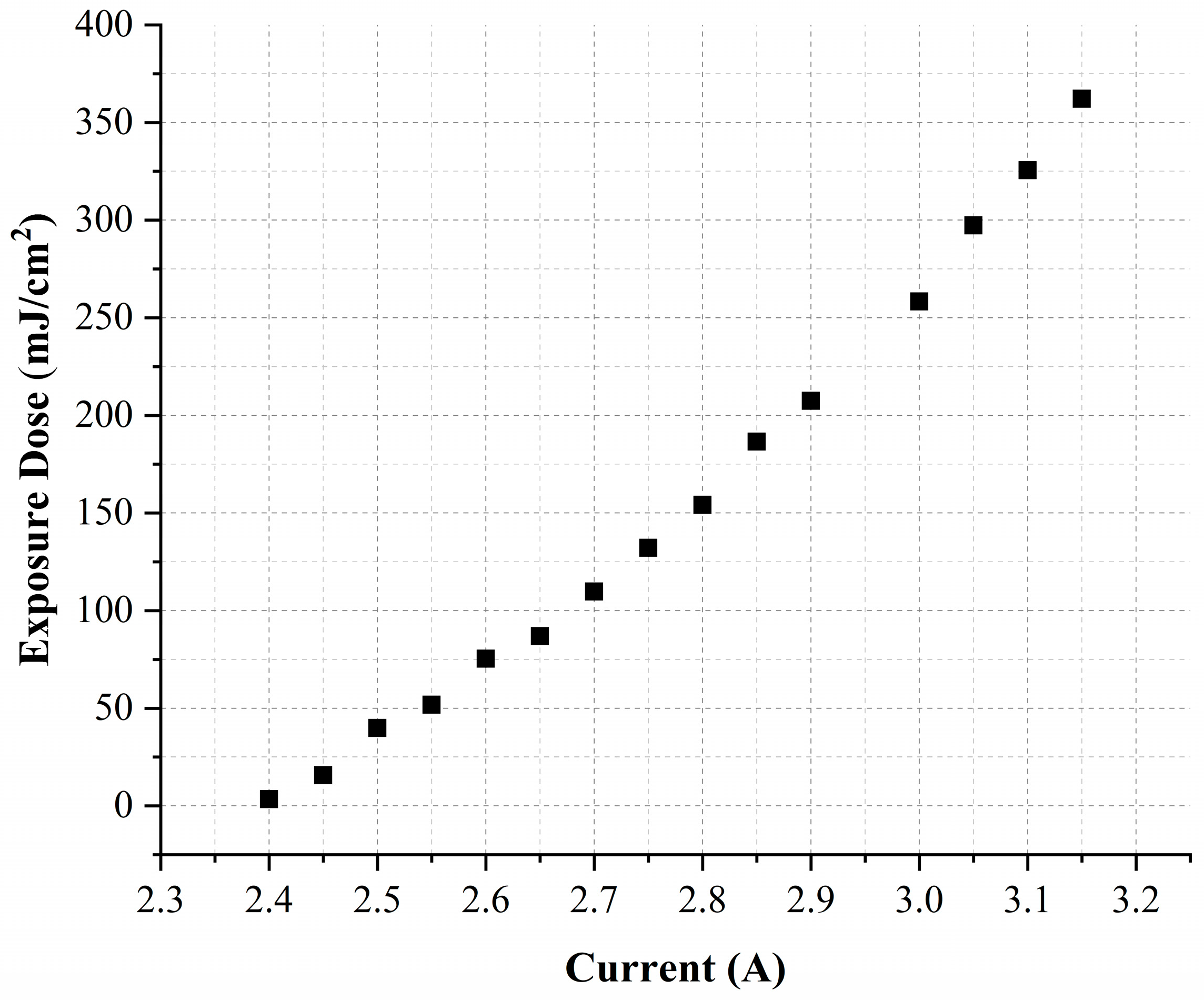
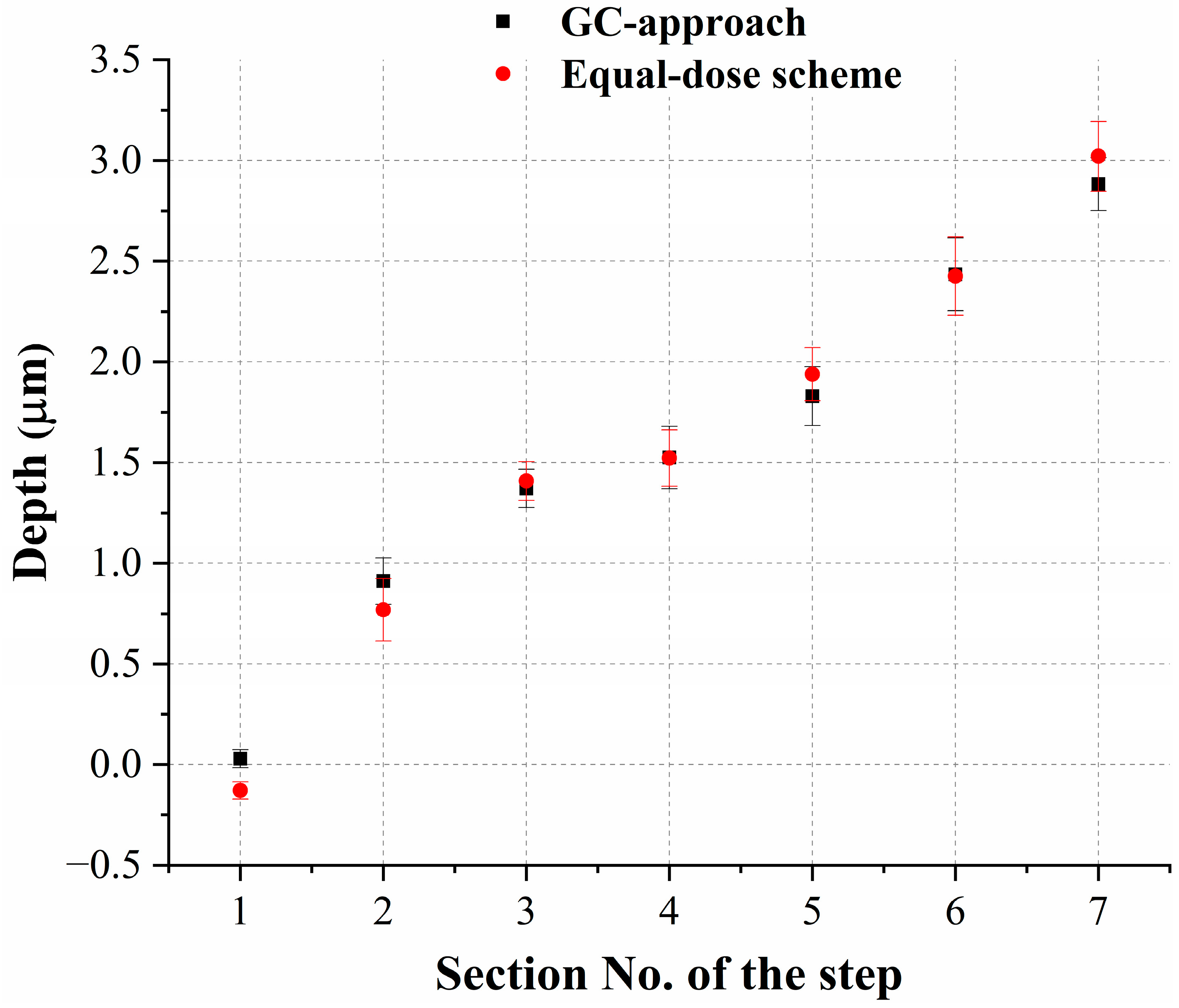
4. The Experimental Results

Two types of experiments were conducted to verify the feasibility of the proposed digitized quasi-3D photolithography: one for 1D multi-step patterns and the other for DOEs, i.e., 2D multi-step patterns.

4.1. One-Dimensional Multi-Step Patterns

For initial experimental verification, a series of 1D step patterns were fabricated using the photolithography method with the GC-approach and compared with an equal-dose scheme (using an equal exposure dose for each exposure).
A seven-step pattern with 1 mm width separations was fabricated using the GC-approach. Driving currents of 2.4 A, 2.72 A, and 3.05 A of the exposure laser were used, respectively, as approximately the basic, twofold, and fourfold exposure doses, as indicated in Figure 1. An additional driving current of 3.15 A was used to emulate the highest exposure intensity (i.e., m ≈ 5 for the Golomb coding). We found a near-logarithmic trend in the depth vs. the exposure dose using laser scanning confocal microscopy (LSCM), as demonstrated in Figure 5. The deviation may have been due to the fluctuation in the LDW system’s output power (0.01~0.1 mW power fluctuations for the same driving current), slight variations in the photoresist, and the measurement error of LSCM.
In the meanwhile, we also compare the GC-approach with the equal-dose scheme with a low m value (m ≈ 3), as shown in Figure 6. The equal-dose scheme exposes the photoresist seven times (29 min in total) using the same dose with the lowest driving current (2.4 A), while only three exposures (12 min in total) are needed for the GC-approach. The measured depth data in Figure 6 reveal that the step patterns for both the GC-approach and the equal-dose exposure scheme have almost the same distribution.
To sum up, both the GC-approach and the equal-dose scheme are able to fabricate 1D multi-step patterns with controlled depth requirements. Moreover, the GC-approach is much more efficient compared to the equal-dose scheme in terms of the exposure time. And this advantage becomes significant for complex structures with large numbers of multi-steps or continuously varying depths. For more precise depth fabrication, careful calibration between the exposure current of the LDW equipment and the exposure depth is necessary, and deep learning algorithms could be introduced for optical proximity correction (OPC) [15,16].

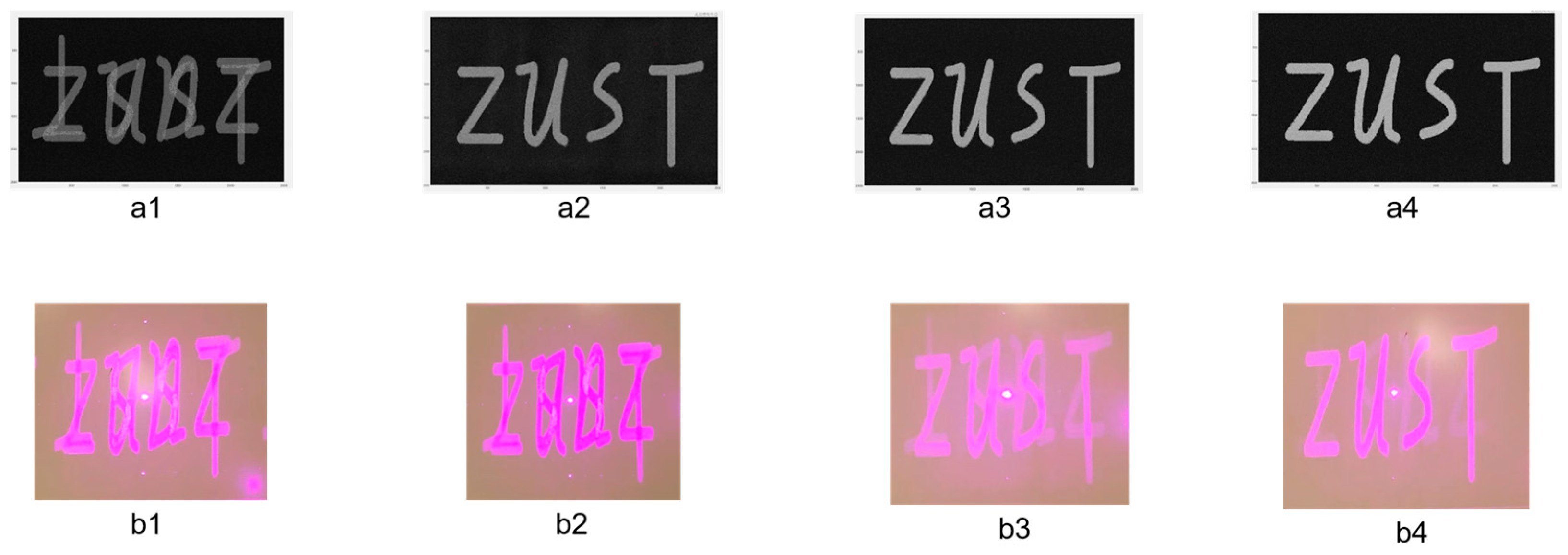
4.2. DOEs—2D Multi-Step Patterns

For further verification of its feasibility, the GC-approach was also applied to fabricating DOE samples with 2D multi-step patterns. For initial verification with medium complexity, the phase distribution was initially computed using the GS algorithm from the original design (Figure 7a) with 500 × 500 pixels (Figure 7b). Then, the depth distribution with the phase incorporated was patterned using 10 µm/pixel with the LDW system, as shown in Figure 7c1–c3. The lateral alignment error in our LDW system in the overlapping exposure is about 20 nm each time, as provided by the LDW system’s manufacturer (SVG Optronics). Here, it can be estimated to be approximately 0.5 µm from Figure 7c3, about 5% of the linewidth (10 µm) for the DOE samples. Further improvements in such alignment errors may involve integrating adaptive optics for precise positioning in real time.
In theory, optimized DOE designs with higher step numbers usually have a higher diffraction efficiency [23]. As a consequence, DOEs with two to five steps were designed using the GS algorithm and fabricated using the GC-approach, as shown in Figure 8. Three driving currents (2.4 A, 2.72 A, and 2.85 A) were used during exposure to generate the basic, twofold, and highest (m ≈ 3) exposure intensities.
Both the simulated diffraction images (Figure 8a1–a4) and the fabricated ones (Figure 8b1–b4) reveal that the diffraction efficiency and clarity of the images were enhanced when the step number increased. Therefore, the GC-approach is very promising for manufacturing accurate micro/nano-optic devices with 2D multi-step structures. Further verification with more complex structures could involve testing MLAs or DOEs with continuously varying phase distributions, i.e., hundreds of steps with different depths instead of five steps at most as seen here.

5. Conclusions

A digitized quasi-3D photolithography method based on a modified Golomb coding was presented for fabricating multi-step micro/nano-optic devices. The proposed approach digitizes the exposure dose of the 3D structure using a grayscale image and then exposes the photoresist via an LDW system with overlaps with the sliced binary images based on a modified Golomb coding. Such digitized quasi-3D photolithography not only removes the multiple developing cycles involved in the traditional fabrication techniques for binary optics but also efficiently utilizes the highest exposure intensity irrespective of the dose distribution. The digitized quasi-3D lithography approach proposed can be used to fabricate DOEs, MLAs, μROEs, etc., and 3D molds for micro-embossing/nano-imprinting.
Currently, the lateral resolution of the GC-approach is about 1 µm, limited by the CD of the LDW system (~1 µm) and the pixel size of the DMD (originally 10.8 µm/pixel and 0.1023 µm/pixel for a single exposure). However, the exposure dose digitalization and image slicing processes are relatively independent of the photolithography system, and the GC-approach proposed here could be extended further to patterning quasi-3D nano-structures using a nano-photolithography system.

Author Contributions

Conceptualization: Z.H. and H.W. Methodology: Z.H. Validation: Z.H. and H.W. Data curation: H.W. Writing—original draft preparation: H.W. Writing—review and editing: Z.H. and S.Z. Supervision: Z.H. and Y.S. Funding acquisition: Z.H. All authors have read and agreed to the published version of the manuscript.

Funding

This research was funded by Zhejiang University of Science and Technology, under grant no. 2020KJ213 and grant no. 0401108N36.

Data Availability Statement

The data underlying the results presented in this paper are not publicly available at this time but may be obtained from the authors upon reasonable request.

Acknowledgments

H.W. and Z.H. would like to acknowledge Guofang Sun for the assistance with the analysis of the samples and discussions. H.W. also would like to acknowledge Zuowei Zhou for the assistance with the sample measurements.

Conflicts of Interest

The authors declare no conflicts of interest.

Abbreviations

The following abbreviations are used in this manuscript:
LDWLaser direct writing
DMDDigital micromirror device
DOEDiffractive optical device
MLAMicrolens array
μROEMicro-refractive optical element
GCGolomb coding
LSCMLaser scanning confocal microscopy

References

  1. Lu, J.; Wu, W.; Colombari, F.M.; Jawaid, A.; Seymour, B.; Whisnant, K.; Zhong, X.; Choi, W.; Chalmpes, N.; Lahann, J.; et al. Nano-achiral complex composites for extreme polarization optics. Nature 2024, 630, 860–865. [Google Scholar] [CrossRef] [PubMed]
  2. Liu, Z.; Hu, G.; Ye, H.; Wei, M.; Guo, Z.; Chen, K.; Liu, C.; Tang, B.; Zhou, G. Mold-free self-assembled scalable microlens arrays with ultrasmooth surface and record-high resolution. Light Sci. Appl. 2023, 12, 143. [Google Scholar] [CrossRef] [PubMed]
  3. Tong, Z.; Niu, F.; Jian, Z.; Sun, C.; Ma, Y.; Wang, M.; Jia, S.; Chen, X. Micro-refractive optical elements fabricated by multi-exposure lithography for laser speckle reduction. Opt. Express 2020, 28, 34597–34605. [Google Scholar] [CrossRef] [PubMed]
  4. Wang, X.; Fan, X.; Liu, Y.; Xu, K.; Zhou, Y.; Zhang, Z.; Chen, F.; Yu, X.; Deng, L.; Gao, H.; et al. 3D nanolithography via holographic multi-focus metalens. Laser Photonics Rev. 2024, 18, 2400181. [Google Scholar] [CrossRef]
  5. Wang, L.; Li, H.; Zhao, C.; Zhang, L.; Li, J.; Din, S.U.; Wang, Z.; Sun, J.; Torres, S.A.G.; Fan, Z.; et al. Aluminum surface work hardening enables multi-scale 3D lithography. Nat. Mater. 2025, 24, 39–47. [Google Scholar] [CrossRef]
  6. Skliutas, E.; Merkininkaitė, G.; Maruo, S.; Zhang, W.; Chen, W.; Deng, W.; Greer, J.; von Freymann, G.; Malinauskas, M. Multiphoton 3D lithography. Nat. Rev. Methods Primers 2025, 5, 15. [Google Scholar] [CrossRef]
  7. Feng, F.; Liu, Y.; Zhang, K.; Yang, H.; Hyun, B.-R.; Xu, K.; Kwok, H.-S.; Liu, Z. High-power AlGaN deep-ultraviolet micro-light-emitting diode displays for maskless photolithography. Nat. Photon. 2025, 19, 101–108. [Google Scholar] [CrossRef]
  8. Qin, N.; Qian, Z.-G.; Zhou, C.; Xia, X.-X.; Tao, T.H. 3D electron-beam writing at sub-15 nm resolution using spider silk as a resist. Nat. Commun. 2021, 12, 5133. [Google Scholar] [CrossRef]
  9. Brown, M.A.; Zappitelli, K.M.; Singh, L.; Yuan, R.C.; Bemrose, M.; Brogden, V.; Miller, D.J.; Smear, M.C.; Cogan, S.F.; Gardner, T.J. Direct laser writing of 3D electrodes on flexible substrates. Nat. Commun. 2023, 14, 3610. [Google Scholar] [CrossRef]
  10. Harinarayana, V.; Shin, Y.C. Two-photon lithography for three-dimensional fabrication in micro/nanoscale regime: A comprehensive review. Opt. Laser Technol. 2021, 142, 107180. [Google Scholar] [CrossRef]
  11. Singhal, A.; Dalmiya, A.; Lynch, P.T.; Paprotny, I. 2-photon polymerized IP-dip 3D photonic crystals for mid IR spectroscopic applications. IEEE Photonics Technol. Lett. 2023, 35, 410–413. [Google Scholar] [CrossRef]
  12. Gonzalez-Hernandez, D.; Varapnickas, S.; Merkininkaitė, G.; Čiburys, A.; Gailevičius, D.; Šakirzanovas, S.; Juodkazis, S.; Malinauskas, M. Laser 3D printing of inorganic free-form micro-optics. Photonics 2021, 8, 577. [Google Scholar] [CrossRef]
  13. Hwang, E.; Hong, J.; Yoon, J.; Hong, S. Direct writing of functional layer by selective laser sintering of nanoparticles for emerging Applications: A Review. Materials 2022, 15, 6006. [Google Scholar] [CrossRef] [PubMed]
  14. Kim, H.-M.; Shin, Y.-K.; Seo, M.-H. Development of shape prediction model of microlens fabricated via diffuser-assisted photolithography. Micromachines 2023, 14, 2171. [Google Scholar] [CrossRef]
  15. Luan, S.; Peng, F.; Zheng, G.; Gui, C.; Song, Y.; Liu, S. High-speed, large-area and high-precision fabrication of aspheric micro-lens array based on 12-bit direct laser writing lithography. Light Adv. Manuf. 2022, 3, 47. [Google Scholar] [CrossRef]
  16. Chen, J.T.; Zhao, Y.-Y.; Guo, X.; Duan, X.-M. Deep learning-driven digital inverse lithography technology for DMD-based maskless projection lithography. Opt. Laser Technol. 2025, 180, 111578. [Google Scholar] [CrossRef]
  17. Choi, J.; Kim, G.; Lee, W.-S.; Chang, W.S.; Yoo, H. Method for improving the speed and pattern quality of a DMD maskless lithography system using a pulse exposure method. Opt. Express. 2022, 30, 22487–22500. [Google Scholar] [CrossRef]
  18. Zhong, K.; Gao, Y.; Li, F.; Luo, N.; Zhang, W. Fabrication of continuous relief micro-optic elements using real-time maskless lithography technique based on DMD. Opt. Laser Technol. 2014, 56, 367–371. [Google Scholar] [CrossRef]
  19. Dinh, D.-H.; Chien, H.-L.; Lee, Y.-C. Maskless lithography based on digital micromirror device (DMD) and double sided microlens and spatial filter array. Opt. Laser Technol. 2019, 113, 407–415. [Google Scholar] [CrossRef]
  20. Gao, Y.; He, S.; Luo, N.; Rao, Y. Research on dynamical-gradual greyscale digital mask lithography. J. Mod. Optic. 2011, 58, 573–579. [Google Scholar] [CrossRef]
  21. Golomb, S. Run-length encodings (Corresp.). IEEE T. Inform. Theory 1966, 12, 399–401. [Google Scholar] [CrossRef]
  22. Stern, M.B. Binary optics: A VLSI-based microoptics technology. Microelectron. Eng. 1996, 32, 369–388. [Google Scholar] [CrossRef]
  23. Levy, U.; Mendlovic, D.; Marom, E. Efficiency analysis of diffractive lenses. J. Opt. Soc. Am. A 2001, 18, 86–93. [Google Scholar] [CrossRef] [PubMed]
Figure 1. The experimentally determined exposure dose (mJ/cm2) of the LDW system with the driving current (A). The refresh rate and the size of the DMD are 6000 Hz and 1920 × 1080 pixels, respectively. An objective lens of 50× is used, and the pixel size is 0.1023 μm/pixel.
Photonics 12 00587 g001
Figure 2. Overall flowchart of steps for proposed quasi-3D photolithography.
Photonics 12 00587 g002
Figure 3. A grayscale image representing the relative exposure dose distribution for the original 3D pattern design. Points a, b, c, d has grayscale level 4, 45, 165, and 200 respectively.
Photonics 12 00587 g003
Figure 4. Binary images obtained through bit plane slicing with the Golomb coding. 1st–6th binary images correspond to images with lower slicing (Seg. 2 of Golomb coding), and 7–10th binary images correspond to images with higher slicing (Seg. 1 of Golomb coding).
Photonics 12 00587 g004
Figure 5. Depth data for the fabricated 7-step pattern with AZ1500 (20 cp) via the GC-approach (m = 5). The depths were measured using LSCM ContourGT-K equipment from Bruker. The exposure dose for each driving current was obtained by averaging the results of five exposure intensity measurements.
Photonics 12 00587 g005
Figure 6. The depth data of the fabricated 7-step patterns with AZ1500 (20 cp) via the GC-approach (m = 3) and equal-dose exposure. Both depths were measured using LSCM ContourGT-K equipment from Bruker.
Photonics 12 00587 g006
Figure 7. Diffractive pattern design, phase distribution, and fabricated samples under a microscope. (a) The original diffractive pattern design; (b) the phase distribution using the GS algorithm; (c1c3) microscope images of fabricated DOE samples magnified 100, 500, and 1000 times, respectively.
Photonics 12 00587 g007
Figure 8. DOE design patterns with different numbers of steps and samples fabricated with the GC-approach. (a1a4) Simulated diffraction images using the GS algorithm with 2- to 5-step microstructures, respectively; (b1b4) diffraction images passing through the DOE samples, corresponding to (a1a4).
Photonics 12 00587 g008
Table 1. The modified Golomb coding for points a–d demonstrated in Figure 3.
PointSeg. 1 of Golomb CodingSeg. 2 of Golomb Coding
a0000000100
b0001000100
c1111000001
d1111100100
Disclaimer/Publisher’s Note: The statements, opinions and data contained in all publications are solely those of the individual author(s) and contributor(s) and not of MDPI and/or the editor(s). MDPI and/or the editor(s) disclaim responsibility for any injury to people or property resulting from any ideas, methods, instructions or products referred to in the content.

