Abstract
Topological photonic crystals have garnered significant attention due to their fascinating topological edge states. These states are robust against sharp bends and defects and exhibit the novel property of unidirectional transmission. In this study, we analyze the topological edge states of gyromagnetic topological photonic crystals in analogy with the quantum Hall effect. Through expanding and shrinking six dielectric cylinders, the optical quantum spin Hall effect is achieved. And helical edge states with pseudo-spin are demonstrated. Owing to the novel topological properties of these edge states, robust waveguides are proposed. Furthermore, integrating these two distinct types of topological states, a novel circulator with topological characteristics is designed. These topologically protected photonic devices will be beneficial for developing integrated circuits.
1. Introduction
Photonic crystals (PCs) are periodic electromagnetic structures that enable the precise manipulation of optical wave propagation. These structures exhibit photonic bandgap characteristics that prohibit the transmission of electromagnetic waves within specific frequency ranges. Though dispersion manipulation, extraordinary optical phenomena can be realized, including slow light propagation and negative refraction effects. Then, these PCs have many applications in optical devices, such as filters, switches, and lasers. But for these conventional PCs, structural and material defects can indeed significantly impact the propagation characteristics of electromagnetic waves. Recently, topological photonic crystals have developed greatly due to their unique properties [1]. Topological edge states with a strong robustness against defects and sharp bends have been realized on varieties of platforms in analogy of the quantum Hall effect (QHE), quantum spin Hall effect (QSHE), and quantum valley Hall effect (VHE) [2,3,4,5,6,7]. According to the bulk-boundary correspondence, topological edge states emerge at the interface between two distinct topological structures. Topological phase transitions can be induced by breaking time-reversal symmetry or spatial inversion symmetry. In the optical QHE system, the Dirac cone was opened by breaking the time-reversal symmetry. The first topological photonic insulator was demonstrated in the gyromagnetic photonic crystals (PCs) with applied magnetic fields [8,9], which can enable one-way, backscattering-immune edge states similar to electronic quantum Hall systems. Subsequently, all-dielectric PCs were introduced to realize the photonic quantum spin Hall insulators. By breaking the symmetry of all-dielectric PCs, the concept of topological spin photonic crystals was first theoretically established and subsequently confirmed through experimental verification [10,11,12]. Analogous to the electronic quantum spin Hall effect (QSHE), spin topological photonic crystals support spin-dependent one-way edge states. In contrast to magnetic topological photonic crystals that depend on magneto–optic effects or external fields, spin topological photonic crystals realize spin–orbit coupling via geometric phase (Berry Phase) or symmetry modulation while preserving time-reversal symmetry. After that, the valley degree of freedom was proposed, and valley PCs were paid more attention. The fundamental principle involves breaking spatial inversion symmetry to create valley-dependent topological edge states within photonic band structures, thereby enabling a low-loss optical transmission with robust backscattering immunity [13,14,15,16,17,18]. So far, numerous topological devices have been proposed, including topological waveguides [19,20,21,22,23], topological optical switches [24,25,26,27], topological delay lines [28,29,30], topological lasers [31,32], topological filters [33], and topological sensors [34]. These devices exhibit a superior performance with weak backscattering characteristics and lower propagation losses. But they are mainly based on utilizing the photonic degrees of spin freedom or valley freedom. In fact, there are remarkable possibilities for robust transport through engineering composite quantum Hall/quantum spin Hall waveguides. However, the topological devices are rarely researched through utilizing both chiral edge states and pseudo-spin states. Especially for the circulator, as a non-reciprocal electromagnetic device, which can enable unidirectional signal transmission, where energy can only flow from one port to another in a specific sequence. Due to its unique non-reciprocal characteristics, circulators play an important role in fields such as communications, radar systems, and integrated photonics. Based on valley photonic crystals, topological circulators were proposed. But they were mainly based on utilizing the photonic degrees of valley freedom and their robustness was limited. In fact, there are remarkable possibilities for robust transport through engineering composite quantum Hall/quantum spin Hall waveguides. However, the topological circulators are rarely researched through utilizing both chiral edge states and pseudo-spin states.
In this paper, we analyze topological edge states of two-dimensional Hall and pseudo-spin–Hall photonic systems. The basic unit cell is composed of six dielectric cylinders. In order to realize the quantum Hall effect, gyromagnetic dielectric cylinders are employed to break the time-reversal symmetry under external magnetic fields. To achieve the photonic quantum spin Hall effect, the topological phase transition can be induced by shrinking and expanding the honeycomb lattice. Here, both types of topological states associated with the chiral edge state and pseudo-spin state are achieved, and their robustness against sharp bends and defects is demonstrated. Additionally, a topological circulator is proposed by identifying a common bandgap between these two different topological structures. Topological edge states appearing at the interface between gyromagnetic PCs and pseudo-spin PCs can propagate smoothly through sharp bends, whereas conventional circulators exhibit strong backscattering when electromagnetic waves encounter sharp bends and defects.
The main contributions of this work are summarized as follows. (1) By introducing magneto–optical materials and lattice deformation simultaneously, hybrid topological phases are achieved in PCs. Topological edge states with unidirectional transmission properties emerge at the interface of these two types of PCs. This unidirectional transmission ensures that light propagates along the interface without backscattering, which is crucial for robust signal transmission. (2) By utilizing the path selection characteristics of distinct topological interfaces, a four-port circulator has been designed to enable the sequential cyclic transmission of electromagnetic waves through the ports. Compared with previous circulators based on magnetic PCs, this configuration achieves both a high transmission efficiency and low backscattering properties. Crucially, only a biased magnetic field is applied to the magnetic photonic crystals in the central region, which simplifies device complexity.
2. Pseudo-Spin Photonic Crystals and Their Topological States
As illustrated in Figure 1a, the unit cell is composed of six dielectric cylinders embedded in air with the lattice constant of a = 18 mm. The dielectric constant is εr = 9.8, and the diameter of the cylinder is d = 4.5 mm. The distance from the center of the cylinder to the center of the hexagonal lattice is denoted as R. Here, TM modes with an out-of-plane electric field and in-plane magnetic field are considered. According to Maxwell’s equation, the eigen equation can be described by
where ε(r) is the position-dependent permittivity, E(r) is the electric field dependent on the position, c is the speed of light, and ω is the frequency of the electromagnetic (EM) wave. Here, the software COMSOL Multiphysics 5.6 is utilized to solve the eigenvalue equation and obtain the band structures of the designed PCs. When calculating the band structure of the unit cell, three pairs of periodic boundary conditions are applied around the hexagonal lattice along its three principal symmetry directions. When a/R = 3, the unit cell is designated as PC0 and is represented by the yellow. In this configuration, the intra-atomic and inter-atomic tunneling between the nearest dielectric cylinders is equivalent, resulting in a system that mimics a honeycomb lattice [10]. As illustrated in Figure 2c, a fourfold degenerate double Dirac cone appears near the Γ point at the frequency of 8.15 GHz. To break the Dirac cone and introduce a complete bandgap, the spacing between adjacent cylinders within the unit cell can be adjusted. Then by setting a/R = 3.5, the unit cell is now designated as PC1 and is represented by the dark red. This adjustment results in a complete bandgap ranging from 7.63 GHz to 8.80 GHz. From the electric field intensity distributions of the eigenstates px, py, dx2 − y2, and dxy at the Γ point, d states are above the p states, so this system can be considered as a nontrivial state [10,12]. But when we set a/R = 2.75, the unit cell is named PC2, denoted by the purple, and there also exists a complete bandgap from 7.71 GHz to 8.65 GHz, as illustrated by Figure 1d. But the topological phase transition appears, as depicted in Figure 1e, where the p states are above the d states. Then we can deduce that PC1 is a topologically trivial structure, whereas PC2 is a topologically nontrivial structure [35]. Notably, they share a common bandgap spanning from 7.71 GHz to 8.65 GHz.
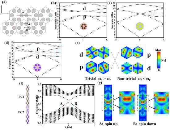
Figure 1.
(a) A schematic diagram of the hexagonal honeycomb lattice PC; (b) the scheme of PC1 and calculated band structure; and (c) the scheme of PC0 and calculated band structure. (d) The scheme of PC2 and calculated band structure; (e) the electric field intensity distributions of PC1 and PC2 at Γ point and their topological phase transition; (f) a supercell composed of the topologically trivial structure PC1 and the topologically nontrivial structure PC2, as well as its projected band structure. The state marked by a pink dot (A) and the state marked by a green dot (B) represent the spin-up and spin-down edge states, respectively; and (g) the electric field intensity distribution and Poynting vector of the spin-up and spin-down edge states.
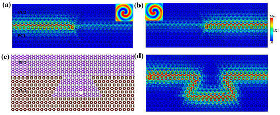
Figure 2.
(a) The leftward unidirectional electromagnetic wave propagation at 8 GHz excited by the LCP chiral source along the interface, and the inset represents the chiral source made by a four-antenna array with a clockwise phase delay between adjacent elements; (b) the rightward unidirectional electromagnetic wave propagation at 8 GHz excited by the RCP chiral source along the interface, and the inset represents the chiral source made by a four-antenna array with a anticlockwise phase delay between adjacent elements. (c) The schematic of the Ω-shaped waveguide constructed by PC1 and PC2, and there exists a defect near the interface. (d) The electric field distributions of topological edge states with the frequency of 8 GHz.
To verify the existence of topological edge states within the system, we have constructed a supercell with 10 unit cells of PC1 and PC2. As illustrated in Figure 1a, the dark red region signifies the topologically trivial structure (PC1), and the purple region represents the topologically nontrivial structure (PC2). When calculating the band structures of the supercell, left and right boundaries along the x-axis are set as periodic boundary conditions, and upper and lower boundaries along the y-axis are set as scattering boundary conditions. We have discerned that there exists a pair of edge states in the bulk bandgap, as illustrated in Figure 1f. There are two edge states labeled as A and B, which have the same frequency of 8 GHz. The electromagnetic energy is mainly confined at the interface between these two structures with different topological phases. The electric field distribution and time-averaged Poynting vectors corresponding to these two eigenstates are presented in Figure 1f. The Poynting vectors direction of edge state A is clockwise, which is characterized as the spin-up edge state. In contrast, the Poynting vectors of edge state B are oriented counterclockwise. Consequently, these two spin edge states will propagate in opposite directions along the interface between the two structures.
In order to evaluate the transmission characteristics of EM waves within the designed structure, we construct a straight waveguide incorporating both the trivial and nontrivial structures, as vividly illustrated in Figure 2a. During the full-wave simulation employed by COMSOL, scattering boundary conditions are applied around the entire structure. To effectively excite the spin edge state, a harmonic source, which consists of four-line sources with a π/2 phase increase/decrease, is placed at the interface between PC1 and PC2. A π/2 phase increase or decrease in the clockwise direction corresponds to a positive or negative orbital angular momentum, respectively. As shown in Figure 2a,b, a left-circularly polarized (LCP) wave carrying a negative orbital angular momentum (OAM) or a right-circularly polarized (RCP) wave carrying a positive OAM can be generated. When the excited source with a frequency of 8 GHz carries an LCP phase vortex, EM waves propagate rightward. But if the excited source with the RCP phase vortex is selected, EM waves propagate leftward. Furthermore, in order to verify the robustness of these helical states, a Ω-shaped waveguide is constructed based on the above structure, as shown in Figure 2c. A source with a frequency of 8 GHz is set at the left port of the waveguide, and the corresponding electric field distribution is plotted in Figure 2c. The results demonstrate that EM waves can pass through the bends smoothly. Even when defects are deliberately introduced near the interface in the designed waveguide, as shown in Figure 2c, the EM wave still has a good one-way transmission along the interface. In contrast, for the conventional waveguide, when the electromagnetic wave encounters bends and defects during the transmission process, severe scattering will occur. This proves that helical edge states are not significantly affected by sharp bends and defects and have a good robustness.
3. Gyromagnetic Photonic Crystals and Their Topological States
In this work, we also exploit the gyromagnetic photonic crystals based on the honeycomb lattice. The unit cell is composed of six yttrium iron garnet (YIG) cylinders with a relative permittivity of εr = 15.26. As shown in Figure 3a, for this particular unit cell designated as PC3, the lattice constant is a = 18 mm. The diameter of each cylinder is r = 0.22a, and the distance between the center of the cylinder and the center of its lattice is R = a/3. We calculate the numerical band structures of the unit cell by employing the commercial software COMSOL Multiphysics. Now, only transverse magnetic (TM) modes are considered. From the band structure of the unit illustrated in Figure 3a, there exists a fourfold degenerate point at the Γ point in the Brillouin zone. To break the degenerate point, an external magnetic field with H = 800 G along the −z axis is applied to break the time-reversal symmetry. The ferrite has a saturation magnetization of 4πMs = 1884 G. Its permittivity is about 15.26, and then the relative permeability tensor of YIG is as follows:
and , is the resonance frequency, and γ = 1.759 × 10¹¹ C/kg is the gyromagnetic ratio. is the characteristic frequency, and H0 is the effective magnetic field in ferrite rods. We choose an operation frequency in a low dispersion region that is far away from the resonance frequency, and then utilize μ = 0.7997 and κ = −0.7155 corresponding to the response of YIG at 8 GHz [36]. This unit cell is denoted as PC4. As presented in Figure 2b, then, there appears a complete bandgap ranging from 7.61 GHz to 8.46 GH. We also construct another kind of unit cell named PC2, which has been discussed above. It also has the constant of the lattice as a = 18 mm. From the band structure of PC2, we can observe that there also exists a complete bandgap between 7.71 GHz and 8.65 GHz. In order to demonstrate the characteristics of the edge states, a supercell with 10 units of both PC1 and PC4 is built. Through analyzing the dispersion cures, we can find that there are edge states marked by the black dots in the bulk bandgap, and topological edge states range from 7.68 GHz to 8.48 GHz. It is worth noting that there is only one forward-propagating mode at the interface. The supercell band calculation demonstrates a single topological edge state traversing the bandgap, where the group velocity maintains a uniform directionality across all frequency points. The magneto–optical effect is realized by breaking the time-reversal symmetry (TRS), inducing a bulk Chern number of C = +1 in the first photonic bandgap (see the band structure calculation in Figure 2c). According to the bulk-boundary correspondence, the interface between PC4 (C = +1) and PC2 (C = 0) must support exactly one chiral edge mode. In addition, a supercell with 10 units of both PC1 and PC4 is also built, and topological edge states range from 7.63 GHz to 8.49 GHz, as shown in Figure 3d. To explore the unique characteristics of the topological edge mode in the designed structure, we construct the Ω-shaped waveguide with gyromagnetic photonic crystals, PC4, and the all-dielectric PC2. The full-wave simulations are also performed by the commercial software COMSOL Multiphysics. As illustrated in Figure 1c, a harmonic source with the frequency of 8 GHz, denoted by the blue star, is placed near the interface at the right port of the waveguide. Scattering boundary conditions are imposed around the whole structure. From the electric field distribution shown in Figure 1d, it can be observed that the EM energy is mainly confined at the domain wall between PC2 and PC4; the EM wave propagates smoothly along the waveguide channel. Remarkably, the EM wave propagates unidirectionally along the waveguide channel with a high transmission efficiency, even when encountering sharp bends. This phenomenon confirms the topological characteristics of topologically edge states. To further assess their robustness to structure defects, a defect (marked by a red star) is intentionally introduced near the waveguide interface. Despite this perturbation, the topological edge states maintained a smooth propagation with minimal distortion, demonstrating their inherent immunity to local imperfections. These numerical results demonstrate that the designed waveguide supports robust topological edge states that are highly resistant to both sharp bends and structural defects, highlighting their potential for applications in photonic devices.
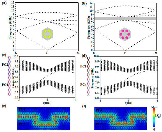
Figure 3.
(a) The scheme of PC3 and the calculated band structure. (b) The scheme of PC4 and the calculated band structure. (c) The scheme of a supercell composed of structures PC2 and PC4 and the projected band structure of the supercell. (d) The scheme of a supercell composed of structures PC1 and PC4 and the projected band structure of the supercell. (e) The schematic of the Ω-shaped waveguide constructed by PC2 and PC4 and the electric field distributions of topological edge states with the frequency of 8 GHz. (f) The schematic of the Ω-shaped waveguide with a defect near the interface and the electric field distributions of topological edge states with the frequency of 8 GHz.
4. Topological Circulator Based on Chiral States and Helical States
The stable unidirectional transmission characteristics of chiral states and helical states have been thoroughly investigated, opening up a novel pathway for the design of highly robust topological devices. Now we have designed a new kind of circulator by utilizing the transmission performance of chiral states and helical states. Based on the aforementioned structure, we propose a circulator that consists of three types of photonic crystals, namely PC0, PC1, and PC2, as illustrated in Figure 4a. Then, there exists the interface between PC1 and PC2, which is denoted as channel 1. Additionally, there is another interface between PC0 and PC1, referred to as channel 2. From the previous analysis, we know that spin edge states emerge at channel 1, while chiral edge states appear at channel 2. These two kinds of edge states propagate unidirectionally along their respective channels. For the designed waveguide, there are four ports labeled as Port 1, Port 2, Port 3, and Port 4. Moreover, four junctions are defined as J1, J2, J3, and J4. We now focus on the frequency range of 7.76 GHz to 8.08 GHz. When the TM waves are excited by a line current source with the frequency of the 8 GHz incident from input Port 1, they can propagate along channel 1, and the energy is mainly confined at the interface between PC1 and PC2. If a magnetic field is applied on the PC0 in the −z direction, TM waves continue to propagate unidirectionally along the straight waveguide even when encountering junction J1. And the energy mainly propagates to Port 2. If the excited source with the frequency of 8 GHz is placed at Port 2, when they come across junction J2, they are coupled into the interface between PC0 and PC1. So, the spin edge states are converted into chiral edge states, and then they pass through junction J3 and propagate toward Port 3. When the input port at Port 3 is excited by a z-polarized electric line source, the excited spin edge states propagate towards Port 4. Similarly, when the input port at Port 4 is excited by a z-polarized electric line source to generate spin edge states, the EM waves can propagate along the bent path toward Port 1. In order to calculate and compare the transmission coefficients from Port 1 to Port 2, from Port 2 to Port 3, from Port 3 to Port 4, and from Port 4 to Port 1, we place four linear probes at the four reference planes (denoted by S1, S2, S3, and S4) perpendicular to the interface. Then the planar density of the power flow at each reference plane is calculated at the operating frequencies and the transmission coefficients. Then S21, S32, S43, and S14 are derived. From the obtained transmission coefficients, it is evident that the proposed circulator can achieve an >80% transmission efficiency with a backscattering suppression below 20% across 7.83–8.06 GHz. Moreover, we further study the transmission properties of edge states under localized defects and random disorder, which are introduced into transmission path from the Port 4 to Port 1. We introduced a defect by removing one unit cell along the transmission path from Port 4 to Port 1, as illustrated in the inset of Figure 4g. The electric field distribution of the transmitted electromagnetic wave shows that the topological edge state can still propagate smoothly. Additionally, disorder was introduced into the transmission channel, as depicted in the inset of Figure 4h. The electric field distribution demonstrates that the topological edge state exhibits a certain degree of immunity to disorder. These results further confirm the robustness of the circulator. A comparison between our work and other relevant circulators based on magnetic PCs reported in the literature is listed in Table 1. But in our work, the integration of magneto–optical effects with a lattice deformation generates novel topological edge states. Utilizing topological interface path selection properties, we demonstrate a four-port circulator enabling the sequential EM wave circulation. Compared with conventional devices based on magnetic photonic crystals, this configuration has unique characteristics against sharp bends and defects and exhibits both a high transmission efficiency and low backscattering properties.
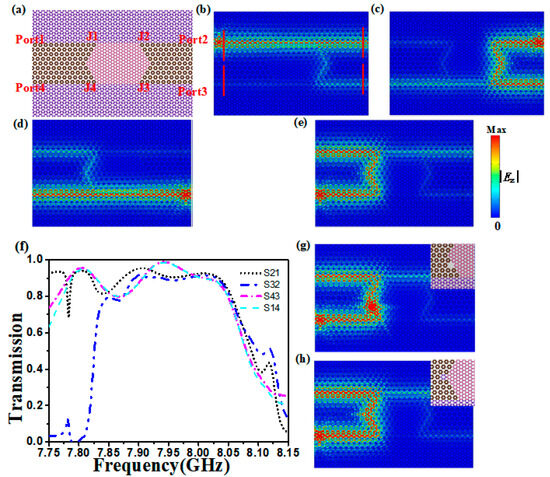
Figure 4.
(a) The schematic diagram of the designed circulator. (b) The electric field distributions of topological edge states with the frequency of 8 GHz propagating from Port 1 to Port 2. S1, S2, S3, and S4 denote four reference planes. (c) The electric field distributions of topological edge states with the frequency of 8 GHz propagating from Port 2 to Port 3. (d) The electric field distributions of topological edge states with the frequency of 8 GHz propagating from Port 3 to Port 4. (e) The electric field distributions of topological edge states with the frequency of 8 GHz propagating from Port 4 to Port 1. (f) The transmission coefficients corresponding to (b–e) are displayed. (g,h) The electric field distributions of topological edge states with the frequency of 8 GHz when the defect and disorder is introduced, respectively.

Table 1.
A comparison between our work and other relevant circulators.
We have mainly theoretically analyzed the topological circulator, and now a realistic experimental design can be used to manufacture the circulator. A circulator composed of magnetic photonic crystals and spin photonic crystals is designed with metallic plates positioned above and below. In the central magnetic photonic crystal region, the upper and lower plates are patterned with honeycomb arrays, which are not fully hollowed out, retaining a thickness to suppress electromagnetic wave leakage along the z-direction. Honeycomb-shaped magnet arrays are embedded into the hexagonal holes of the metallic plates (fixed with non-magnetic materials such as aluminum alloys) to prevent magnet displacement caused by magnetic pole interactions. A bias magnetic field is generated via magnets. Cylindrical magnets with a radius larger than those of the YIG cylinders are designed to ensure uniform magnetic fields around the YIG cylinders in the z-direction [40,41].
5. Conclusions
In conclusion, we have engineered hexagonal honeycomb photonic crystals. Within these crystals, based on all-dielectric photonic crystals (PCs), two distinct types of topological edge states are present. Chiral edge states are achieved in gyromagnetic photonic crystals when an external magnetic field is applied. On the other hand, spin edge states emerge at the interface between a topologically trivial structure and a topologically nontrivial structure, which is realized by expanding and shrinking the honeycomb lattice. Then these two edge states have emerged as promising candidates for optical communication and integrated photonic devices, owing to their robustness and unidirectional transmission characteristics. By integrating chiral edge states and pseudo-spin-polarized modes through interfacial bandgap control, we demonstrate a topological circulator achieving a high transmission efficiency, suppressed backscattering, and defect immunity, surpassing the constraints of conventional designs. It can achieve robust signal routing with >80% transmission efficiency and a backscattering suppression below 20% across 7.83–8.06 GHz. Crucially, the device requires only a localized bias magnetic field applied to the central magnetic photonic crystal region, thereby eliminating auxiliary control circuits and reducing structural complexity. These features are expected to open up new avenues for the development of potential applications in optical and gigahertz devices, offering promising prospects for advancements in this field.
Author Contributions
Methodology, Y.Z. and F.L.; software, Y.Z. and J.H.; validation, H.H., J.L., W.Z. and X.T.; writing—original draft preparation, Y.Z. and F.L. All authors have read and agreed to the published version of the manuscript.
Funding
This work was supported by the Science Foundation of Chengdu Aeronautic Polytechnic (ZZX0624081), National Science Foundation of China (62171082), and China Postdoctoral Science Foundation (2024M764271).
Data Availability Statement
Data are contained within the article.
Conflicts of Interest
Authors Yulin Zhao and Xiangjun Tan were employed by the company Avic Chengdu CAIC Electronics Co., Ltd. Author Weihao Zhang was employed by the company The 29th Research Institute of China Electronics Technology Group Corporation. The remaining authors declare that the research was conducted in the absence of any commercial or financial relationships that could be construed as a potential conflict of interest.
References
- Maleki, M.J.; Soroosh, M.; Parandin, F.; Haddadan, F. Photonic Crystal-Based Decoders: Ideas and Structures. In Recent Advances and Trends in Photonic Crystal Technology, 2nd ed.; Goyal, A.K., Kumar, A., Eds.; IntechOpen: London, UK, 2024. [Google Scholar]
- Ozawa, T.; Price, H.M.; Amo, A.; Goldman, N.; Hafezi, M.; Lu, L.; Rechtsman, M.C.; Schuster, D.; Simon, J.; Zilberberg, O.; et al. Topological photonics. Rev. Mod. Phys. 2019, 91, 15006. [Google Scholar] [CrossRef]
- Hasan, M.Z.; Kane, C.L. Colloquium: Topological insulators. Rev. Mod. Phys. 2010, 82, 3045–3067. [Google Scholar] [CrossRef]
- Xie, B.Y.; Wang, H.F.; Zhu, X.Y.; Lu, M.H.; Wang, Z.D.; Chen, Y.F. Photonics meets topology. Opt. Express 2018, 26, 24531–24550. [Google Scholar] [CrossRef] [PubMed]
- Ma, S.; Anlage, S.M. Microwave applications of photonic topological insulators. Appl. Phys. Lett. 2020, 116, 250502. [Google Scholar] [CrossRef]
- Xue, H.; Yang, Y.; Zhang, B. Topological Valley Photonics: Physics and Device Applications. Adv. Photonics Res. 2021, 2, 2100013. [Google Scholar] [CrossRef]
- Tang, G.J.; He, X.T.; Shi, F.L.; Liu, J.W.; Chen, X.D.; Dong, J.W. Topological Photonic Crystals: Physics, Designs, and Applications. Laser Photonics Rev. 2022, 16, 2100300. [Google Scholar] [CrossRef]
- Wang, Z.; Chong, Y.; Joannopoulos, J.D.; Soljačić, M. Reflection-Free One-Way Edge Modes in a Gyromagnetic Photonic Crystal. Phys. Rev. Lett. 2008, 100, 013905. [Google Scholar] [CrossRef]
- Wang, Z.; Chong, Y.; Joannopoulos, J.D.; Soljacic, M. Observation of unidirectional backscattering-immune topological electromagnetic states. Nature 2009, 461, 772–775. [Google Scholar] [CrossRef]
- Wu, L.H.; Hu, X. Scheme for Achieving a Topological Photonic Crystal by Using Dielectric Material. Phys. Rev. Lett. 2015, 114, 223901. [Google Scholar] [CrossRef]
- Barik, S.; Miyake, H.; DeGottardi, W.; Waks, E.; Hafezi, M. Two-dimensionally confined topological edge states in photonic crystals. New J. Phys. 2016, 18, 113013. [Google Scholar] [CrossRef]
- Yang, Y.; Xu, Y.F.; Xu, T.; Wang, H.X.; Jiang, J.H.; Hu, X.; Hang, Z.H. Visualization of a Unidirectional Electromagnetic Waveguide Using Topological Photonic Crystals Made of Dielectric Materials. Phys. Rev. Lett. 2018, 120, 217401. [Google Scholar] [CrossRef]
- Ma, T.; Shvets, G. All-Si valley-Hall photonic topological insulator. New J. Phys. 2016, 18, 025012. [Google Scholar] [CrossRef]
- Dong, J.W.; Chen, X.D.; Zhu, H.; Wang, Y.; Zhang, X. Valley photonic crystals for control of spin and topology. Nat. Mater. 2017, 16, 298–302. [Google Scholar] [CrossRef]
- Chen, X.D.; He, X.T.; Dong, J.W. All-Dielectric Layered Photonic Topological Insulators. Laser Photonics Rev. 2019, 13, 1900091. [Google Scholar] [CrossRef]
- He, X.T.; Liang, E.T.; Yuan, J.J.; Qiu, H.Y.; Chen, X.D.; Zhao, F.L.; Dong, J.W. A silicon-on-insulator slab for topological valley transport. Nat. Commun. 2019, 10, 872. [Google Scholar] [CrossRef] [PubMed]
- Liu, Y.; Chen, X.; Xu, Y. Topological Phononics: From Fundamental Models to Real Materials. Adv. Funct. Mater. 2019, 30, 1904784. [Google Scholar] [CrossRef]
- Wang, H.; Gupta, S.K.; Xie, B.; Lu, M. Topological photonic crystals: A review. Front. Optoelectron. 2020, 13, 50–72. [Google Scholar] [CrossRef]
- Chen, Q.; Zhang, L.; Xu, S.; Wang, Z.; Li, E.; Yang, Y.; Chen, H. Robust waveguiding in substrate-integrated topological photonic crystals. Appl. Phys. Lett. 2020, 116, 231106. [Google Scholar] [CrossRef]
- Yoshimi, H.; Yamaguchi, T.; Ota, Y.; Arakawa, Y.; Iwamoto, S. Slow light waveguides in topological valley photonic crystals. Opt. Lett. 2020, 45, 2648–2651. [Google Scholar] [CrossRef]
- Chen, Q.; Zhang, L.; Chen, F.; Yan, Q.; Xi, R.; Chen, H.; Yang, Y. Photonic Topological Valley-Locked Waveguides. ACS Photonics 2021, 8, 1400–1406. [Google Scholar] [CrossRef]
- Yu, X.; Chen, J.; Li, Z.Y.; Liang, W. Topological large-area one-way transmission in pseudospin-field-dependent waveguides using magneto-optical photonic crystals. Photonics Res. 2023, 11, 1105–1112. [Google Scholar] [CrossRef]
- Han, J.F.; Liang, F.; Zhao, Y.L.; Liu, J.; Wang, S.; Wang, X.R.; Zhao, D.S.; Wang, B.Z. Valley kink states and valley-polarized chiral edge states in substrate-integrated topological photonic crystals. Phys. Rev. Appl. 2024, 21, 014046. [Google Scholar] [CrossRef]
- Shalaev, M.I.; Desnavi, S.; Walasik, W.; Litchinitser, N.M. Reconfigurable topological photonic crystal. New J. Phys. 2018, 20, 023040. [Google Scholar] [CrossRef]
- Song, Z.; Liu, H.; Huang, N.; Wang, Z. Electrically tunable robust edge states in graphene-based topological photonic crystal slabs. J. Phys. D Appl. Phys. 2018, 51, 304003. [Google Scholar] [CrossRef]
- Cao, T.; Fang, L.; Cao, Y.; Li, N.; Fan, Z.; Tao, Z. Dynamically reconfigurable topological edge state in phase change photonic crystals. Sci. Bull. 2019, 64, 814–822. [Google Scholar] [CrossRef] [PubMed]
- Liu, X.; Huang, J.; Chen, H.; Qian, Z.; Ma, J.; Sun, X.; Fan, S.; Sun, Y. Terahertz topological photonic waveguide switch for on-chip communication. Photonics Res. 2022, 10, 1090–1096. [Google Scholar] [CrossRef]
- Liu, J.W.; Shi, F.L.; He, X.T.; Tang, G.J.; Chen, W.J.; Chen, X.D.; Dong, J.W. Valley photonic crystals. Adv. Phys. X 2021, 6, 1905546. [Google Scholar] [CrossRef]
- Lan, Z.; Chen, M.L.N.; Gao, F.; Zhang, S.; Sha, W.E.I. A brief review of topological photonics in one, two, and three dimensions. Rev. Phys. 2022, 9, 100076. [Google Scholar] [CrossRef]
- You, J.W.; Lan, Z.; Ma, Q.; Gao, Z.; Yang, Y.; Gao, F.; Xiao, M.; Cui, T.J. Topological metasurface: From passive toward active and beyond. Photonics Res. 2023, 11, 1090–1096. [Google Scholar] [CrossRef]
- Zeng, Y.; Chattopadhyay, U.; Zhu, B.; Qiang, B.; Li, J.; Jin, Y.; Li, L.; Davies, A.G.; Linfield, E.H.; Zhang, B.; et al. Electrically pumped topological laser with valley edge modes. Nature 2020, 578, 246–250. [Google Scholar] [CrossRef]
- Liu, X.; Zhao, L.; Zhang, D.; Gao, S. Topological cavity laser with valley edge states. Opt. Express 2022, 30, 4965–4977. [Google Scholar] [CrossRef] [PubMed]
- Gu, L.; Yuan, Q.; Zhao, Q.; Ji, Y.; Liu, Z.; Fang, L.; Gan, X.; Zhao, J. A Topological Photonic Ring-Resonator for On-Chip Channel Filters. J. Light. Technol. 2021, 39, 5069–5073. [Google Scholar] [CrossRef]
- Navaratna, N.; Tan, Y.J.; Kumar, A.; Gupta, M.; Singh, R. On-chip topological THz biosensors. Appl. Phys. Lett. 2023, 123, 033705. [Google Scholar] [CrossRef]
- Bernevig, B.A.; Hughes, T.L.; Zhang, S.-C. Quantum Spin Hall Effect and Topological Phase Transition in HgTe Quantum Wells. Science 2006, 314, 1757–1761. [Google Scholar] [CrossRef]
- Xi, X.; Ye, K.P.; Wu, R.X. Influence of bias magnetic field direction on band structure of magnetic photonic crystal and its role in constructing topological edge states. Acta Phys. Sin. 2020, 69, 154102. [Google Scholar] [CrossRef]
- Xu, B.; Zhang, D.; Zeng, X.; Wang, Y.; Dong, Z. Wideband Y-Type Circulator Based on Magneto Photonic Crystals and Triangular Ferrites. IEEE Photonics Technol. Lett. 2019, 31, 743–746. [Google Scholar] [CrossRef]
- Anandan, S.; Vani, D.; Gupta, P.; Krishnan, P. A Low Loss Hexagonal Six-Port Optical Circulator Using Silicon Photonic Crystal. Opt. Quantum Electron. 2023, 55, 1092. [Google Scholar] [CrossRef]
- Xu, B.; Zhang, D.; Wang, Y.; Hong, B.; Shu, G.; He, W. A Terahertz Circulator Based on Magneto-Photonic Crystal Slab. Photonics 2023, 10, 360. [Google Scholar] [CrossRef]
- Chen, J.; Liang, W.; Li, Z.-Y. Antichiral One-Way Edge States in a Gyromagnetic Photonic Crystal. Phys. Rev. B 2020, 101, 214102. [Google Scholar] [CrossRef]
- Han, J.; Liang, F.; Zhao, Y. Highly Efficient Conversion from Classical Guided Waves to Topological Chiral Edge States. Chin. Opt. Lett. 2024, 22, 023902. [Google Scholar] [CrossRef]
Disclaimer/Publisher’s Note: The statements, opinions and data contained in all publications are solely those of the individual author(s) and contributor(s) and not of MDPI and/or the editor(s). MDPI and/or the editor(s) disclaim responsibility for any injury to people or property resulting from any ideas, methods, instructions or products referred to in the content. |
© 2025 by the authors. Licensee MDPI, Basel, Switzerland. This article is an open access article distributed under the terms and conditions of the Creative Commons Attribution (CC BY) license (https://creativecommons.org/licenses/by/4.0/).