1. Introduction
Surface plasmon polaritons (SPPs) are hybrid electromagnetic excitations that arise from the strong interaction between the incident light and collective oscillations of free electrons at the boundary between a metal and a dielectric medium. This interaction is predominantly driven by the collective oscillations of surface electrons excited by the incoming light, resulting in the formation of a hybrid wave, commonly known as a surface plasmon wave [
1]. Under such excitation, the electric field is strongly localized at the metal–dielectric interface, this significantly enhances the coupling between the electromagnetic wave and surface electrons. Owing to their unique sub-wavelength characteristics and strong field enhancement, SPPs have found widespread applications in optics, nanophotonics, and high-sensitivity sensing.
As SPPs travel parallel to the metal–dielectric interface, their electric field diminishes quickly in the direction perpendicular to the surface, effectively confining energy to the nanoscale regime [
2]. Compared with conventional optical waves, SPPs exhibit shorter wavelengths, which endows them with considerable potential for the design of micro- and nanostructures. Key parameters, such as propagation length, resonance frequency, and coupling efficiency, can be tuned by varying the metal type, film thickness, and surface morphology [
3]. A variety of SPP-based nanostructures have been developed, including nanopore arrays, nanoslots, nanospheres, and nanorods [
4,
5,
6,
7]. These structures not only enable precise modulation of local SPP behavior but also achieve strong field enhancement effects, facilitating applications in surface-enhanced spectroscopy, nanomanipulation, sensor development, and nanophotonic device integration [
8].
SPP can be excited at various metal–dielectric interfaces, including metal–insulator–metal (MIM) waveguides [
9] and dielectric–metal–dielectric setups [
10]. Among them, MIM waveguides have superior field confinement and re-reduced ohmic loss, which make them attractive platforms for long-distance SPP propagation [
11]. The MIM straight waveguide coupled with the slow-light effect is one of the typical schemes for realizing the slow-light, and it is commonly used to enhance the sensitivity of liquid or gas sensors, to enhance the nonlinear effect, and to improve the light-delay characteristics [
12]. In addition to this, MIM waveguides have been configured with a series of coupled cavities, such as keyed resonant cavities, conical cavities with defects, side-coupled circular cavities, and 8-resonant cavities with triangular truncation lines, to form nanorefractive index sensors [
13,
14,
15,
16].
Among the diverse optical interference effects observed in plasmonic waveguide-coupled systems, Fano resonance is particularly notable [
17]. This phenomenon, initially discovered in atomic systems, arises from the interference between discrete and continuum states, resulting in destructive interference and zero absorption at specific frequencies [
18]. In SPP systems, Fano resonance emerges from the interference between bright and dark modes. The bright modes are directly excited by incident light in the MIM waveguide and exhibit broad, flat spectral features, while the dark modes, present in the metallic nanostructures, are only excited through coupling with bright modes and produce narrow spectral features [
19]. When these modes spectrally overlap and interfere, an asymmetric line shape characteristic of Fano resonance is observed [
20]. Compared to traditional plasmonic resonances, Fano resonances exhibit narrower linewidths and enhanced local electromagnetic fields, resulting in superior sensitivity to environmental variations and structural perturbations, making them highly suitable for sensing applications [
21].
In this paper, a novel nanoscale refractive index sensor is proposed, which is based on a ring resonant cavity generated by coupling a MIM waveguide with a DSR configuration. The optical transmission behavior of the sensor is explored by finite element method (FEM) simulation [
22] and further analyzed using coupled mode theory (CMT) [
23]. The simulation results show that the asymmetric resonance profile of the DSR originates from the interference between the broadband continuous modes of squares and circles in the MIM waveguide and the narrowband discrete modes supported by the DSR cavity. Given that the DSR resonance is closely related to the cavity geometry, a detailed parametric study is performed. The key structural parameters considered include the radius R2 of the upper and lower circular segments of the DSR, the outer radius R1, the side lengths of the lower-left and lower-right square elements, and the coupling spacing between the MIM waveguide and the DSR, g. The results of the study provide a comprehensive theoretical framework and design guidance for realizing high sensitivities and quality factors for refractive index sensing applications.
2. Structure and Methodology
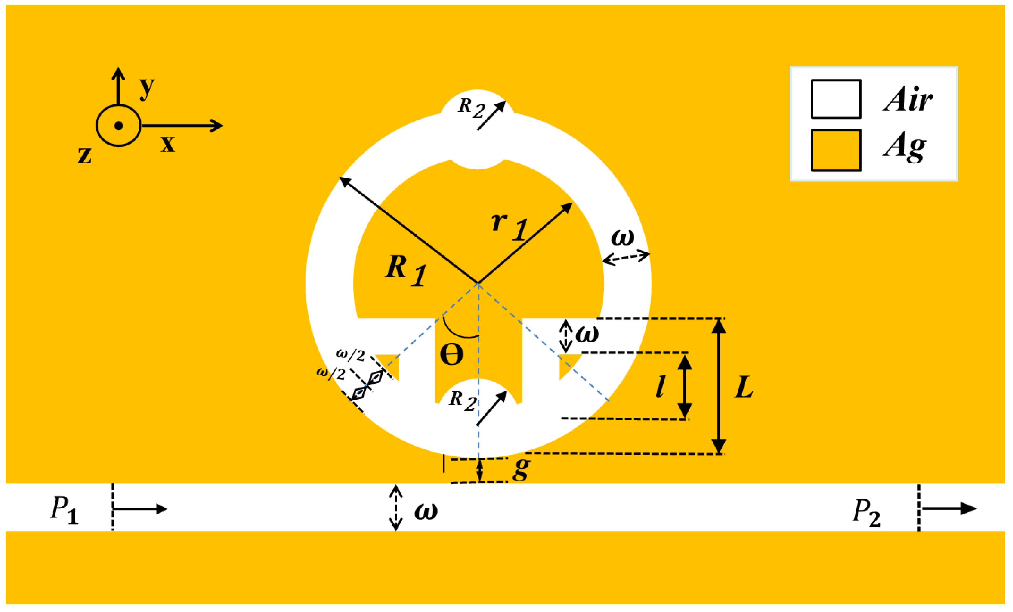
Figure 1 presents a schematic of the proposed structure. The overall configuration comprises a MIM waveguide featuring rectangular barriers, alongside a resonant cavity formed by a DSR structure with circular segments. To reduce computational complexity and hardware requirements, a two-dimensional model is employed for simulation. This simplification is justified by the negligible difference in magnetic field characteristics between two-dimensional and three-dimensional structures in such plasmonic systems.
The DSR cavity is formed by an external circular ring with radius R1 and an internal circular ring with radius r1, with nm; both rings are concentric. Square elements are embedded in the lower-left and lower-right regions of the cavity, defined by outer and inner side lengths L and l, respectively, with a side length difference of 100 nm between them, both having the same geometric center. The upper and lower circular arcs, each with radius , are symmetrically positioned along the central axis of the annular ring.
Let g denote the coupling distance between the MIM waveguide and the DSR cavity, while ω represents the constant width of the MIM waveguide, the rectangular barriers, and the coupling interfaces. To ensure the excitation of only the fundamental symmetric mode within the MIM waveguide, the dielectric layer width is fixed at 50 nm throughout the simulation.
Figure 1 illustrates the air and silver (Ag) regions, represented by the white and yellow areas, respectively. Determine the relative permittivity of air
and of silver according to Equation (1), as follows [
24]:
Equation (2) represents the transverse magnetic mode equation for the MIM waveguide, as follows:
where equations
,
,
, and
represent the dielectric constants of the dielectric and metal, respectively. The wave vector within the waveguide is denoted by
k, and in free space, it is expressed as
in free space.
To assess the sensing performance, the following three critical parameters are introduced in this study: full width at half maximum (FWHM), S, and figure of merit (FOM). The FWHM, which quantifies the sharpness of the spectral response, is defined as the spectral bandwidth measured at half of the peak intensity. Sensitivity (S) quantifies the responsiveness of the sensor, typically expressed in units of Refractive Index Unit
−1(RIU
−1), indicating the wavelength shift per unit change in refractive index. The FOM combines both the FWHM and sensitivity to provide an overall measure of performance. The formulas for these parameters are given in Equations (3) and (4), as follows [
25,
26]:
The geometric structure of the sensor system was simulated using COMSOL Multiphysics 5.4a, with and denoting the variations in wavelength and refractive index, respectively. To minimize reflections, a perfect matching layer (PML) was incorporated. The mesh was finely refined in the waveguide and DSR structure regions using ultra-detailed triangular elements to accurately capture the intricate geometry. In other regions, orthogonal triangles were employed for meshing to balance computational accuracy with efficiency. Simulations were conducted over a wavelength range from 1800 nm to 2800 nm, with 1 nm increments, to thoroughly explore the optical behavior of the sensor. This simulation approach ensures the capture of all relevant optical effects across a broad wavelength spectrum, providing a comprehensive assessment of sensor performance.
3. Computational Results and Interpretation
We have systematically analyzed the DSR structures by tuning the parameters of each structure to assess their role on the sensor performance. In addition, the coupling effect between the waveguide and the parameters of the DSR structures was investigated. Comparative results indicated that, within a specified range of refractive index variation, the sensitivity of the DSR structure was enhanced by approximately 500 times compared to the single-ring configuration. Moreover, the DSR structure exhibited a significantly higher FOM, establishing it as a more promising candidate for further investigation.
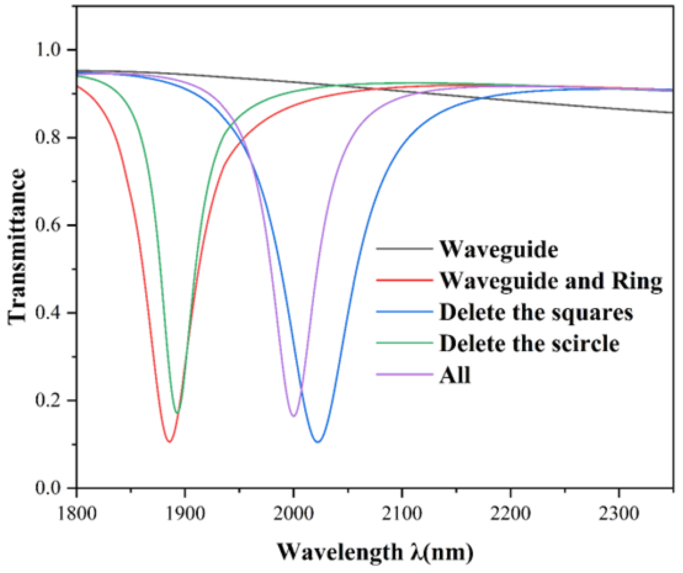
We initialize the parameters of each part of the sensor, as follows: R1 = 240 nm, R2 = 50 nm, L = 70 nm, and g = 10 nm. To further elucidate the formation mechanism of Fano resonance and the electromagnetic propagation behavior of the overall structure, numerical simulations were performed on both the decoupled DSR configuration and the isolated rectangular baffle, as depicted in
Figure 2. The black, red, blue, green, and violet curves correspond to the transmission spectra of the waveguide alone, the single circular ring, the circular ring coupled with a smaller circular element, the circular ring coupled with a square element, and the complete DSR structure, respectively.
As can be seen from the figure, the transmission spectrum of the whole system shows an asymmetric and sharp pattern, indicating the presence of the Fano resonance, which originates from the interference between the continuous broadband mode and the discrete narrowband mode. The transmission spectrum of the single waveguide structure presents a slightly downward sloping straight line with high transmittance at all wavelengths, representing the continuous broadband mode. The straight waveguide-coupled DSR structure, on the other hand, shows a symmetric concave feature and exhibits typical Lorentz resonance characteristics, which can be regarded as a discrete narrowband mode for generating the Fano resonance.
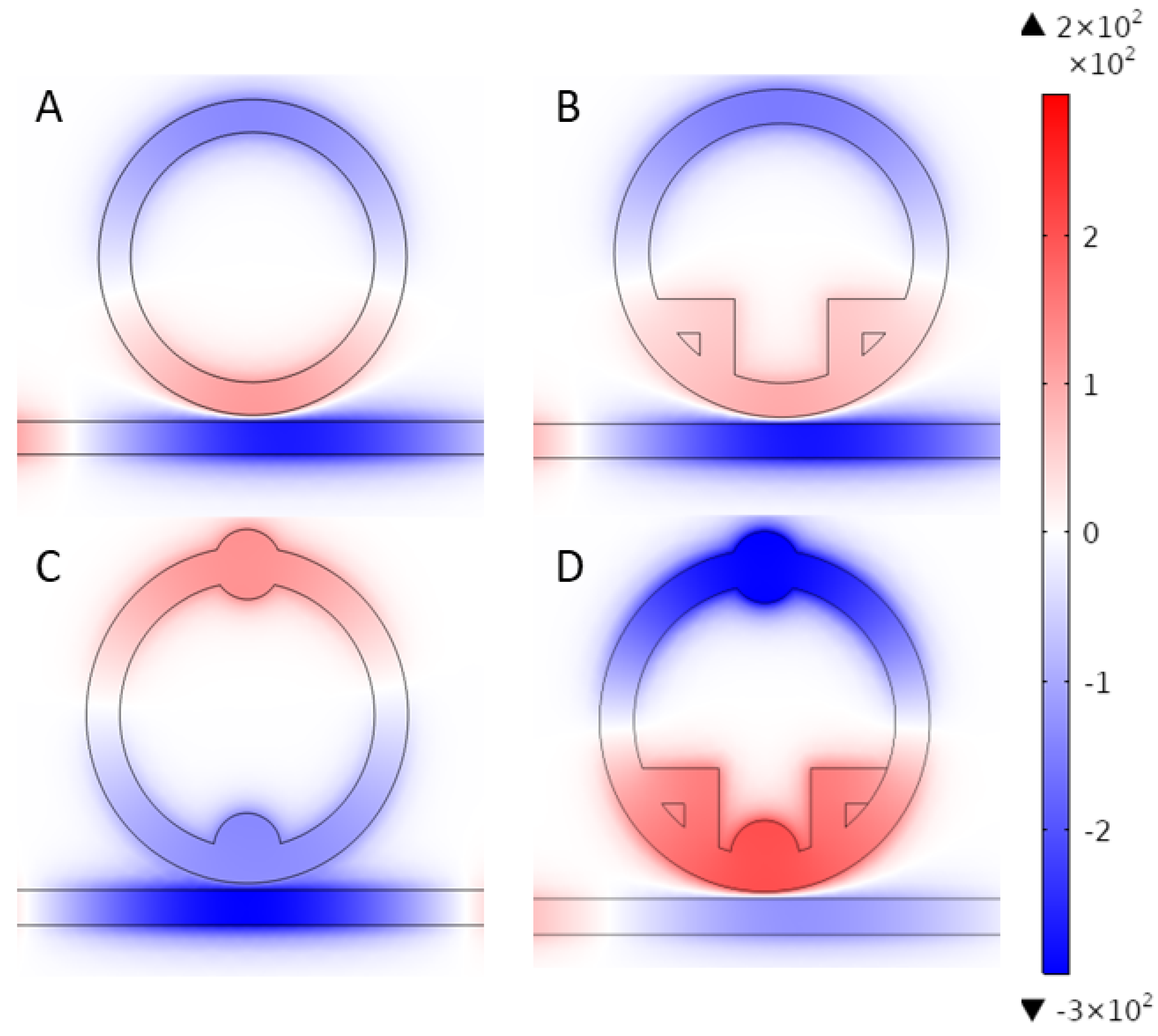
We analyzed the magnetic field distribution for four configurations, namely, a single toroidal structure, a combination of a toroidal structure and a square structure, an integration of a toroidal structure with a small circular structure, and a DSR structure, as shown in
Figure 3A–D. From these figures, it can be seen that, in all four configurations, the magnetic field propagates through the waveguide and is effectively coupled to the structure. The color distribution in
Figure 3A–D indicates the magnetic field distribution, and the color bar on the right is the magnetic field strength per unit. Positive and negative values correspond to the direction and magnitude of the magnetic field relative to a reference axis.
In
Figure 3A, the normalized magnetic field is primarily concentrated in the upper and lower parts of the rings, with the overall magnetic field being weak and mainly confined to the bus waveguide. In
Figure 3B,C, the addition of extra structures to the circular ring results in an enhanced magnetic field distribution, indicating that the additional structures facilitate the coupling of the SPPs. As can be seen in
Figure 3D, only a small portion of the normalized magnetic field is present in the waveguide, and most of the field is concentrated inside the DSR structure, suggesting that a significant resonance occurs. The magnetic field in the DSR structure exhibits a top–bottom distribution with anti-phase characteristics. The field distributions converge symmetrically with the addition of the two structures, leading to a notable increase in coupling strength.
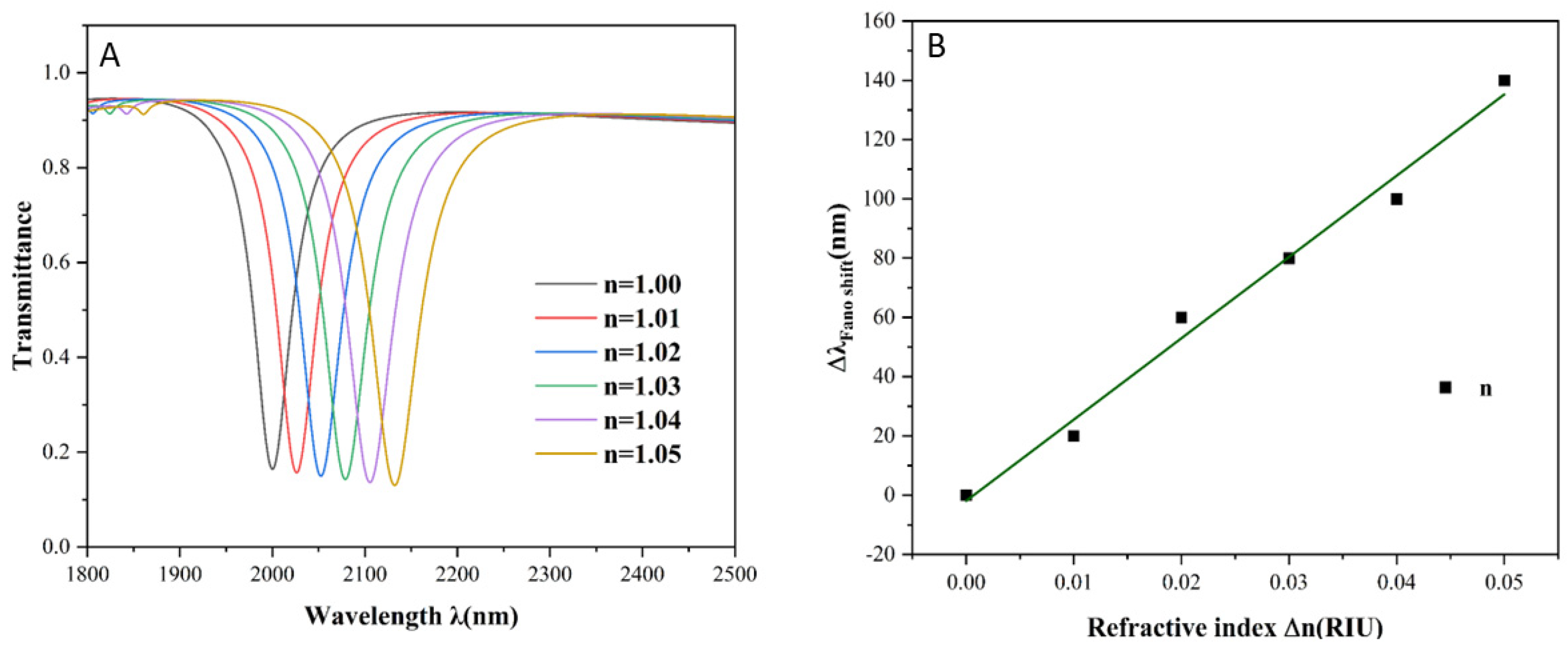
To evaluate the sensing performance of the double-square-ring (DSR) structure, the effect of the refractive index variation was systematically investigated. The structural parameters were fixed as follows: R1 = 240, R2 = 50 , L = 70 nm, g = 10 nm, and ω = 50 nm. Simulations were conducted for refractive indices n = 1.00, 1.01, 1.02, 1.03, 1.04, and 1.05 RIU, and the results are illustrated in
Figure 4A,B. As shown in
Figure 4A, the transmission spectra exhibit a consistent redshift with increasing refractive index, while maintaining the overall spectral profile. This observation indicates that refractive index variation leads primarily to a spectral shift rather than a change in spectral shape. The apparent linear relationship between resonance wavelength and refractive index in
Figure 4B illustrates the reliability of the structure for refractive index sensing applications.
Through the linear fitting of the resonance wavelength shifts, the sensor’s sensitivity is determined to be 2700 nm/RIU. The resulting FOM achieves a peak value of 54, demonstrating that the proposed structure delivers outstanding sensing performance when optimized parameters are applied.
Because the geometry has a large effect on the Fano resonance, we analyze the whole structure in detail. Initially, the effect of the outer radius R1 of the DSR structure was studied. By varying R1 from 220 nm to 240 nm in 5 nm increments, while keeping all other parameters constant, as shown in
Figure 5A, the transmittance at the resonance inclination increases gradually as R1 increases. Furthermore, a noticeable redshift in the resonance wavelength is observed, highlighting the significant role of R1 in determining the Fano resonance position. The corresponding sensitivities, determined through linear fitting, are presented in
Figure 5B. As R1 increases, the sensitivity improves from 1794 nm/RIU to 1999 nm/RIU. These findings suggest that adjusting R1 provides a flexible means to optimize the sensor’s sensitivity for various applications.
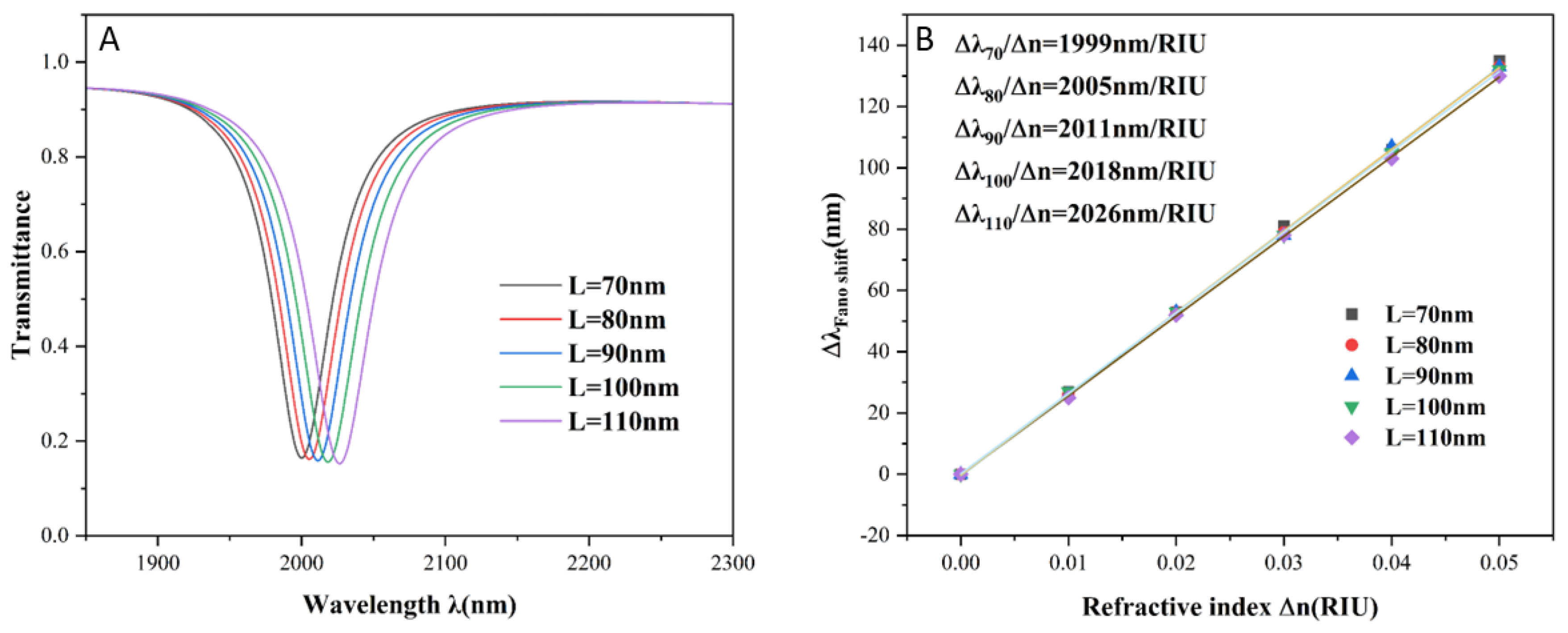
We also investigated the effect of another structural parameter of the DSR on the sensor, in particular the side length of the square element located underneath the DSR. Keeping all other parameters constant, the side length L was varied from 70 nm to 110 nm in 10 nm increments. The resulting transmission spectra and corresponding sensitivity fitting curves are presented in
Figure 6A and
Figure 6B, respectively. From
Figure 6A, it is evident that the overall shape of the spectrum remains largely unchanged as L increases, while a slight redshift in the transmission spectrum is observed.
Figure 6B shows a small increase in sensitivity as L increases. This suggests that the side length can be adjusted according to design specifications with minimal impact on the sensor’s performance.
We proceeded to investigate the effect of the radius R2 of the circular element in the DSR structure on the transmission characteristics of the sensor. The radius R2 is varied from 30 nm to 50 nm in increments of 5 nm with all other parameters held constant. The transmission spectra and sensitivity fitting curves are shown in
Figure 7A and
Figure 7B, respectively. As shown in
Figure 7A, the transmittance at the resonance point decreases with increasing R2, and the resonance wavelength is red-shifted. According to
Figure 7B, the S increases from 1911 nm/RIU to 1999 nm/RIU with the increase in R2, which indicates that R2 affects the performance of the DSR structure, and therefore, adjusting R2 according to the actual sensitivity requirement is a feasible way to optimize the performance of the sensor.
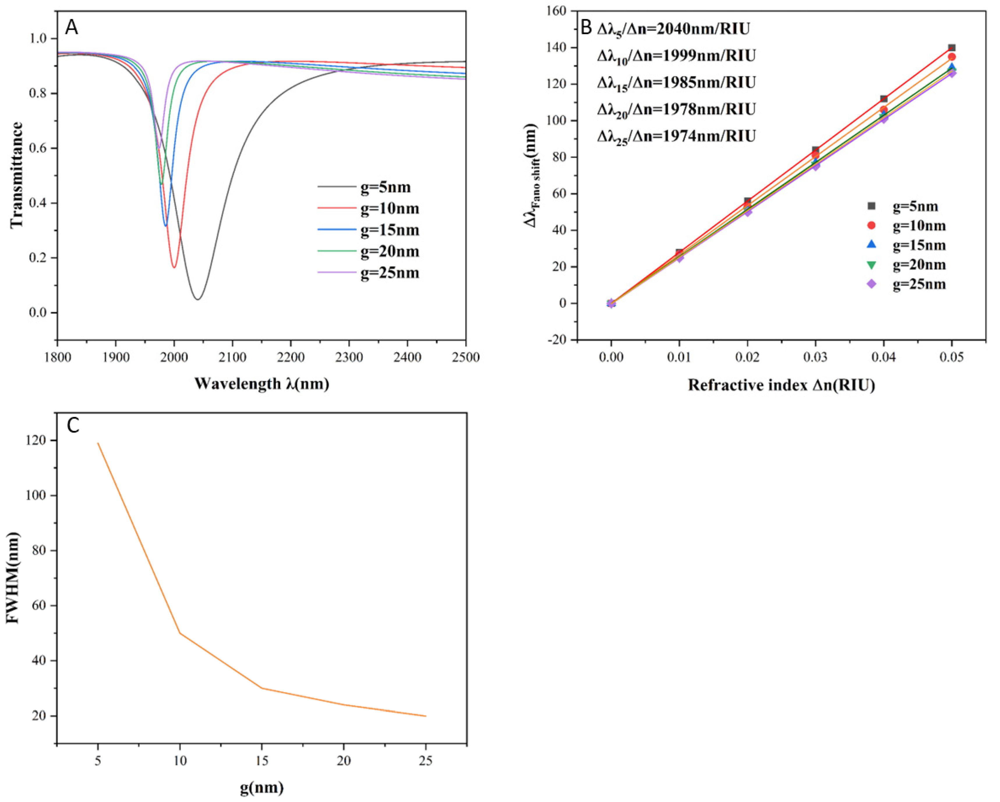
Finally, we investigate the effect of the coupling gap g between the waveguide and the DSR structure on the transmission characteristics. As illustrated in
Figure 8A,B, increasing g from 5 nm to 25 nm results in a pronounced blue shift in the transmission spectrum, accompanied by a gradual decline in sensitivity. The highest sensitivity of 2040 nm/RIU is achieved when g = 5 nm.
Figure 8C reveals that the FWHM narrows significantly with increasing g. However, the FWHM at g = 5 nm remains relatively broad, leading to a reduction in the FOM. Therefore, an optimal trade-off between sensitivity and spectral resolution is attained when g = 10 nm, at which point the sensor exhibits a sensitivity of 2700 nm/RIU and a corresponding FOM of 54.
Table 1 summarizes the performance parameters of other reported structures. Generally, there exists a trade-off between sensitivity and FOM, as increasing the sensitivity tends to broaden the spectral response, thereby reducing the FOM. As a result, most structures exhibit relatively low sensitivity when achieving a high FOM. To ensure both high responsiveness and high detection resolution in sensing applications, it is essential to achieve an optimal balance between these two parameters. Moreover, a well-balanced combination of sensitivity and FOM is more practically valuable, as it provides a reliable and stable sensing performance under real-world operating conditions.
4. Application in Temperature Sensing
Considering the design of the DSR structure, ethanol was deliberately selected as the sensing medium due to its excellent thermo-optic coefficient of 3.94 × 10
−4 °C
−1, which renders the structure highly sensitive and stable for temperature sensing applications. In comparison, the thermo-optic coefficients of silver and quartz are significantly lower, at 8.60 × 10
−6 °C
−1 and 9.30 × 10
−6 °C
−1, respectively. These values are negligible relative to that of ethanol, allowing the influence of temperature on the refractive indices of silver and quartz to be reasonably ignored. This strategic material choice ensures the operational efficiency and reliability of the DSR-based sensor, laying a solid foundation for high-performance temperature sensing. Within the temperature range between the melting point (−144 °C) and boiling point (78 °C) of ethanol, its refractive index is linearly related to temperature and can be described by Equation (5), as follows [
31]:
where
T represents the ambient temperature, and
denotes the reference room temperature, set at 20 °C.
Considering the melting and boiling points of ethanol, the operating temperature range of the temperature sensor was set between −80 °C and 70 °C to ensure optimal performance. Although ethanol has a melting point of −144 °C, the lowest measurable temperature for the sensor was expected to be −130 °C. Temperatures outside the range of −80 °C to 70 °C would degrade the sensor’s accuracy and increase the measurement error. The structural parameters were defined as follows: R₁ = 240 nm, R₂ = 50 nm, L = 70 nm, ω = 50 nm, and g = 10 nm. The refractive index of the temperature sensing medium exhibits high sensitivity to temperature fluctuations. Therefore, the sensor’s operating principle utilizes the spectral shift in transmittance to calculate changes in the refractive index of ethanol, enabling precise temperature detection. This principle of operation provides the sensor with high sensitivity and accuracy, making it a reliable tool for temperature measurement. The sensitivity of the temperature sensor
can be calculated using Equation (6), as follows [
32]:
where
denotes the shift in the transmission spectrum, and
represents the temperature change, which is set to 150 °C according to the test temperature range. The temperature was incrementally increased from −80 °C to 70 °C in steps of 30 °C, with the test results presented in the figure above. As illustrated in
Figure 9A, the transmission spectra exhibit a pronounced blue shift as the temperature rises. Modern optical instruments, capable of nanometer-level precision, allow for accurate wavelength detection. The valley shift observed ranges from 2982 nm to 3178 nm, yielding a spectral shift of
= 196 nm.
Figure 9B presents the sensitivity fit line of the sensor, which ensures measurement accuracy through linear fitting. The calculated sensitivity of the temperature sensor is 1.3 nm/°C.

 ,
, 


