Article

High-Speed Terahertz Modulation Signal Generation Based on Integrated LN-RMZM and CPPLN

by
Hangfeng Zhou
1,
Miao Ma
1,
Chenwei Zhang
2,
Xinlong Zhao
1,
Weichao Ma
3,4,
Wangzhe Li
3 and
Mingjun Xia
2,*
1
School of Information Science and Engineering, Zhejiang Sci-Tech University, Hangzhou 310018, China
2
College of Information Science and Electronic Engineering, Zhejiang University, Hangzhou 310027, China
3
Aerospace Information Research Institute, Chinese Academy of Sciences, Beijing 100190, China
4
Guangdong Provincial Key Laboratory of Terahertz Quantum Electromagnetics, GBA Branch of Aerospace Information Research Institute, Chinese Academy of Sciences, Guangzhou 510700, China
*
Author to whom correspondence should be addressed.
Photonics 2025, 12(5), 490; https://doi.org/10.3390/photonics12050490
Submission received: 11 April 2025 / Revised: 7 May 2025 / Accepted: 13 May 2025 / Published: 15 May 2025
(This article belongs to the Section Optoelectronics and Optical Materials)

Abstract

:
With the increasing communication frequencies in 6G networks, high-speed terahertz (THz) modulation signal generation has become a critical research area. This study first proposes an on-chip high-speed THz modulation signal generation system based on lithium niobate (LN), which integrates a pair of racetrack resonator-integrated Mach–Zehnder modulators (RMZMs) with a chirped periodically poled lithium niobate (CPPLN) waveguide. The on-chip system combines near-infrared electro-optic modulation and cascaded difference-frequency generation (CDFG) for high-speed THz modulation signal generation. At 300 K, utilizing two input optical waves at frequencies of 193.55 THz and 193.14 THz, this on-chip system enables high-speed THz modulation signal generation at 0.41 THz, with a 1 Gbit/s modulation rate and a 0.25 V modulation voltage. During the simulation, when the intensity of the input optical waves is 1000 MW/cm2, the generated 0.41 THz signal reaches a peak intensity of 21.24 MW/cm2. Furthermore, based on theoretical analysis and subsequent simulation, the on-chip system is shown to support a maximum modulation signal generation rate of 7.75 Gbit/s. These results demonstrate the potential of the proposed on-chip system as a compact and efficient solution for high-speed THz modulation signal generation.

1. Introduction

Electromagnetic waves have become the primary medium for modern information transmission. Within the electromagnetic spectrum, THz waves spanning 0.1–10.0 THz exhibit high penetration, low photon energy, and strong potential for high-speed wireless communication [1,2,3,4,5,6]. These properties make THz waves promising for advanced 6G communication and precision detection technologies [7,8,9,10,11,12,13]. Therefore, developing efficient THz modulation signal generation techniques is essential for the practical implementation of THz systems across various fields.
However, current THz modulation signal generation technologies face constraints due to the large physical size of conventional systems and the inherent limitations of modulation materials, such as low electro-optic efficiency and poor phase-matching characteristics [14,15,16]. These challenges arise from the long wavelengths of THz waves, which often require bulky and complex architectures [14]. In particular, state-of-the-art THz modulation signal generation approaches based on artificial electromagnetic metamaterials are unsuitable for on-chip integration, as they function as spatial light modulators. These approaches also face challenges, including complex structural designs, high fabrication costs, and significant insertion losses [15,16]. In contrast, on-chip THz modulation signal generation systems offer enhanced integrability but currently exhibit critical limitations. Key challenges include high modulation voltages (>6 V), limited modulation capability to kHz-range electrical signals, and relatively low generated THz signal intensity [17,18,19,20,21]. These limitations impede the widespread deployment of practical THz modulation signal generation technologies.
To address these challenges, this study first proposes an on-chip high-speed THz modulation signal generation system, which integrates near-infrared electro-optic modulation with CDFG. This on-chip system is based on LN, a material known for its high electro-optic coefficient and low optical loss [22,23]. Specifically, the proposed on-chip system consists of a pair of near-infrared RMZMs and a CPPLN waveguide. Each RMZM employs a resonator to reduce the modulation voltage. Meanwhile, the CPPLN waveguide optimizes the phase-matching conditions for CDFG, enhancing the THz signal generation intensity. At 300 K, utilizing two input optical waves at frequencies of 193.55 THz and 193.14 THz, this on-chip system enables high-speed THz modulation signal generation at 0.41 THz, with a 1 Gbit/s modulation rate and a 0.25 V modulation voltage. When the intensity of the input optical waves is 1000 MW/cm2, the generated 0.41 THz signal reaches a peak intensity of 21.24 MW/cm2. Theoretical analysis indicates that the maximum modulation signal generation rate supported by the on-chip system is 7.75 Gbit/s.

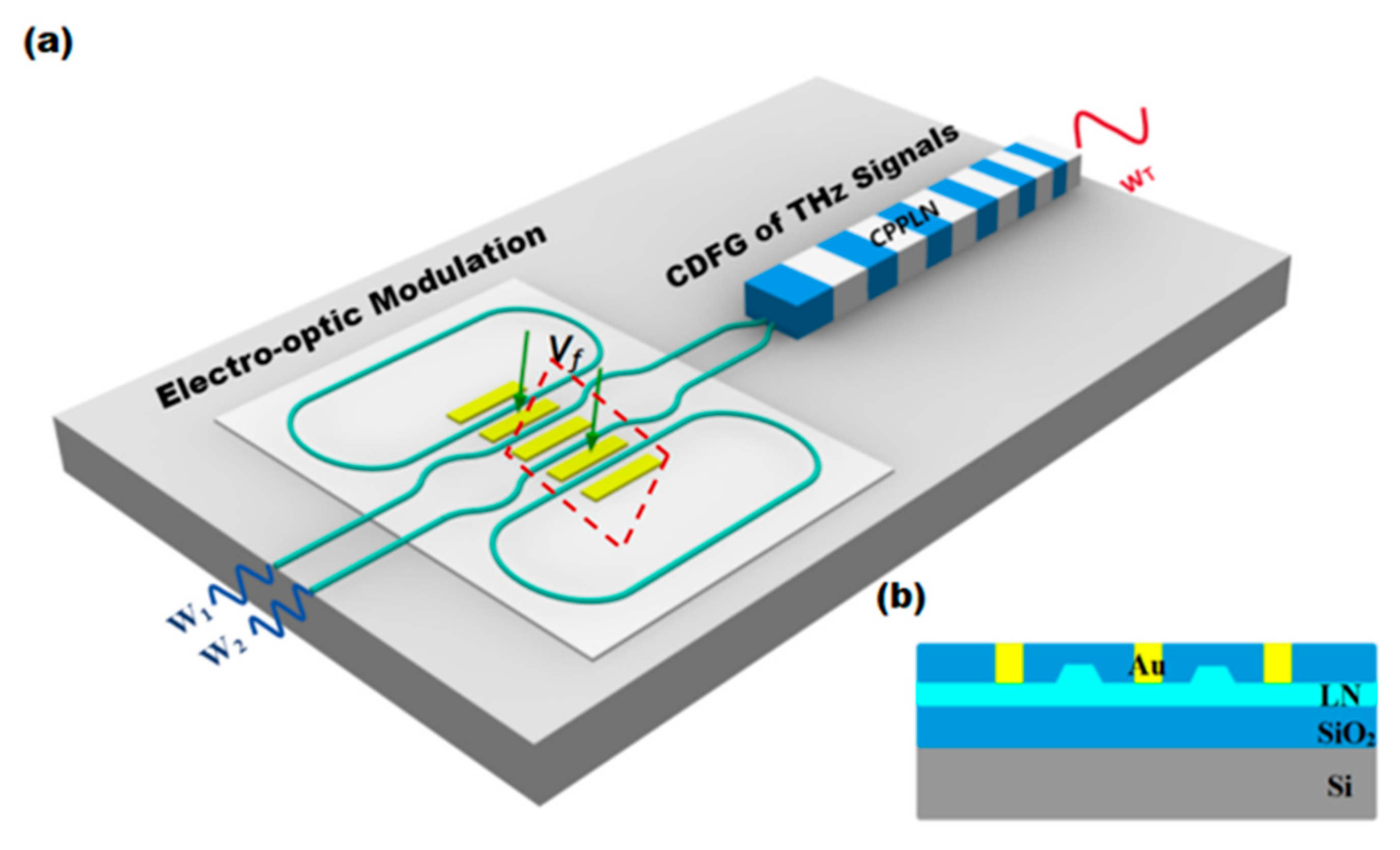
2. Materials and Methods

The proposed on-chip THz modulation signal generation system, depicted in Figure 1a, incorporates a compact architecture, enabling high-speed THz modulation signal generation. This on-chip system consists of two functional modules: an electro-optic modulation unit based on RMZM and a CDFG unit based on CPPLN. In the electro-optic modulation stage, two co-polarized optical waves with closely spaced frequencies ( ω 1 = 193.55   T H z , ω 2 = 193.14   T H z ) are injected into separate RMZMs. Under applied voltages, the RMZMs modulate the incident optical waves. The modulated optical waves are then coupled into the CPPLN waveguide. Here, the chirped poling period compensates for the phase mismatch between cascaded optical frequency components, enabling efficient THz signal ( ω T = ω 1 ω 2 = 0.41   T H z ) generation. This on-chip system enables the generation of modulated THz signals by indirectly modulating two input near-infrared optical waves.

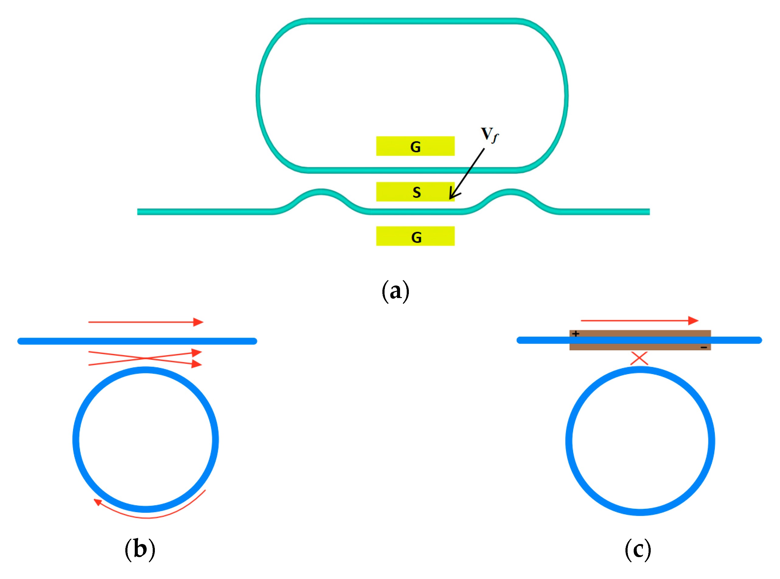
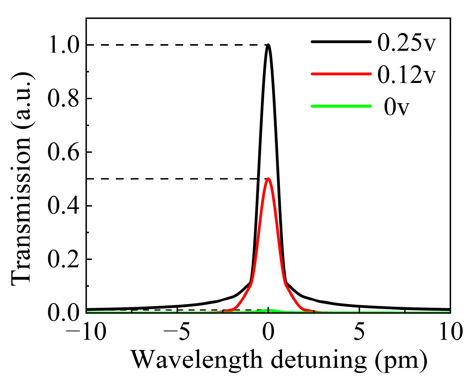
2.1. Electro-Optic Modulation

To minimize on-chip system footprint and power consumption [24,25], this study employs an RMZM architecture for the electro-optic modulation unit, as shown in Figure 2a. The RMZM is implemented on a x-cut thin-film LN layer integrated into a LN-on-insulator platform. The design parameters of the RMZM include a microring radius of 4 mm and a modulation length of 2 cm, the gap of the electrode is 1.8 um. The RMZM enables electro-optic modulation by dynamically tuning the coupling state of the racetrack resonator through an applied voltage V f .
First, under critical coupling conditions (Figure 2b), the input optical wave is almost completely absorbed by the resonator, resulting in near-zero transmission at the resonant wavelength. Upon application of a control voltage, the RMZM is progressively tuned from critical coupling to the zero-coupling regime (Figure 2c), where decoupling of the optical field between the bus waveguide and the racetrack resonator eliminates resonant interactions.
The integrated Mach–Zehnder interferometer operates in a push–pull configuration with complementary phase modulation in its dual arms, enabling rapid suppression of optical transmission through voltage reversal. The applied voltage induces refractive index modulation in the LN waveguide, dynamically altering the resonator coupling conditions. As shown in Figure 3, at V f = 0.25   V , the RMZM enables zero-coupling operation with nearly 100% transmission efficiency; at V f = 0   V , the RMZM establishes critical coupling with nearly 0% transmission. With a modulation length of 2 cm, the electro-optic modulation section gets a V π L of 0.5 V·cm.

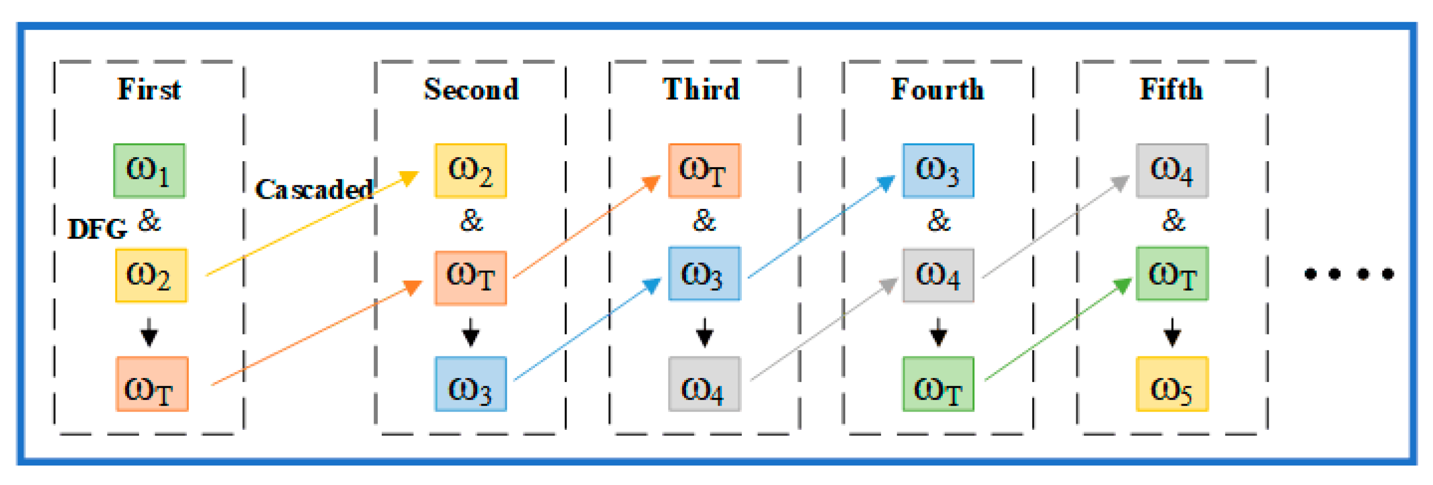
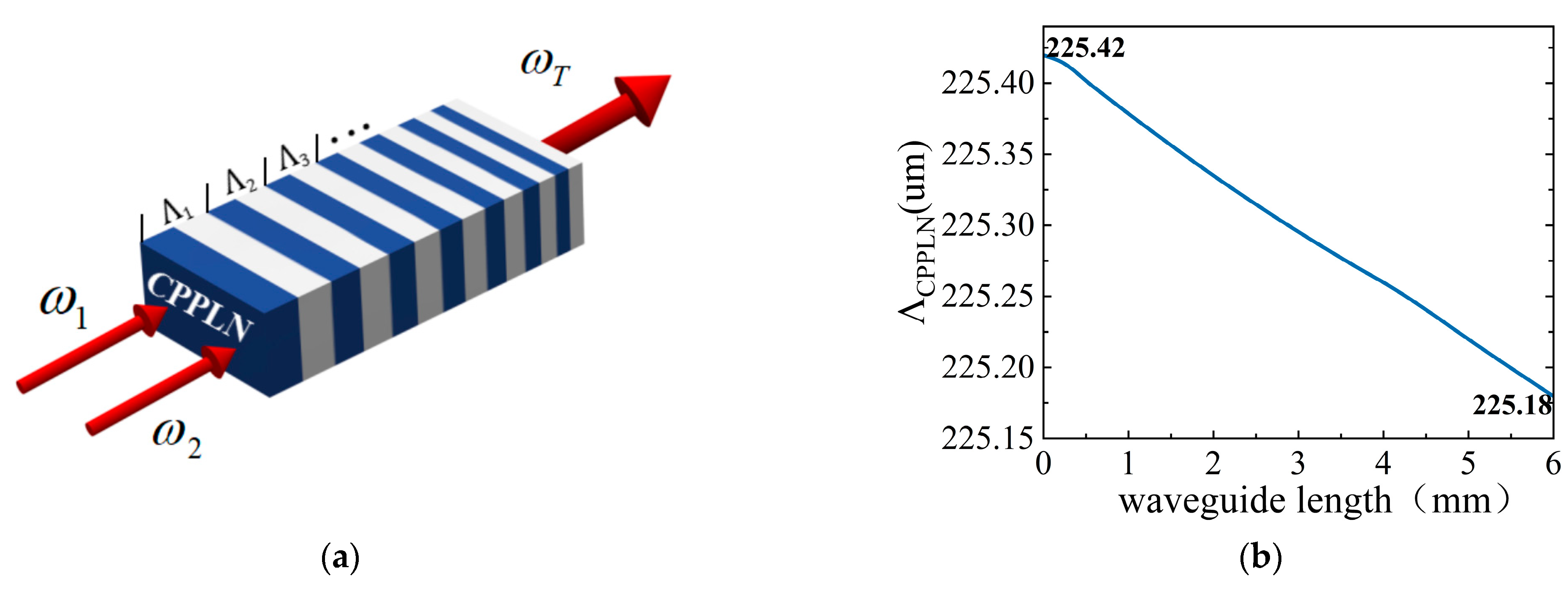
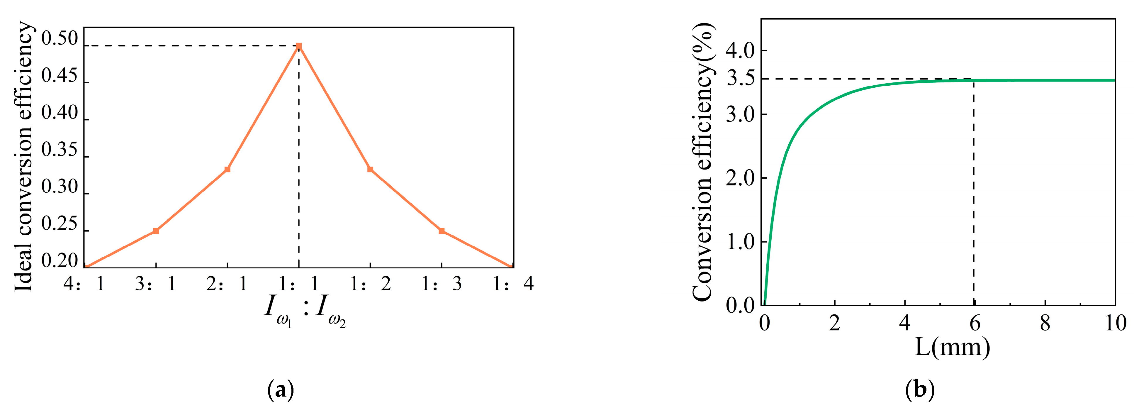
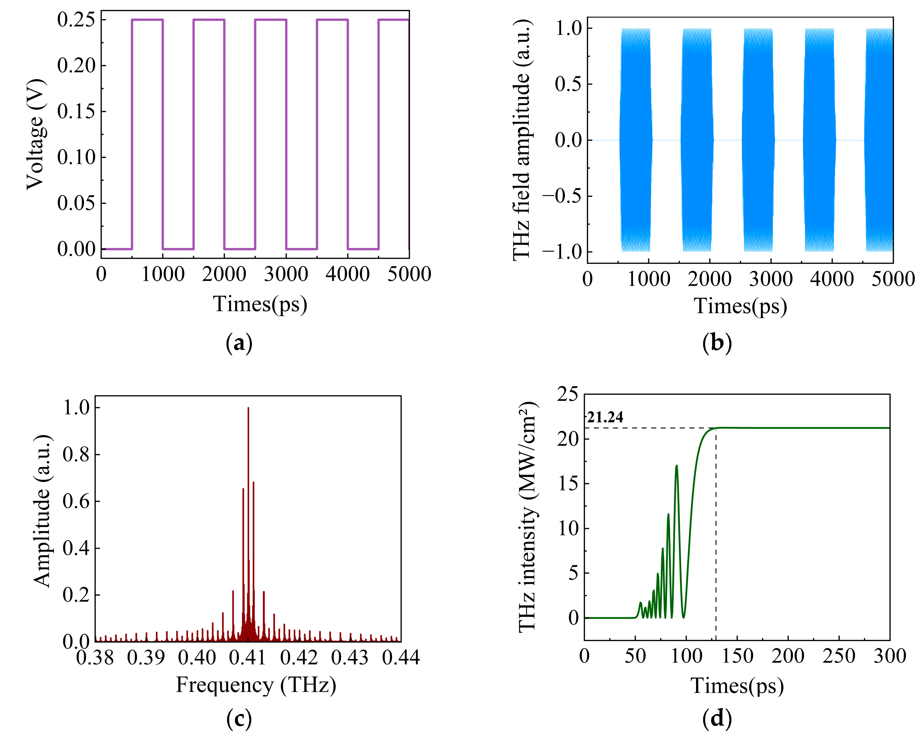
2.2. CDFG of THz Signals
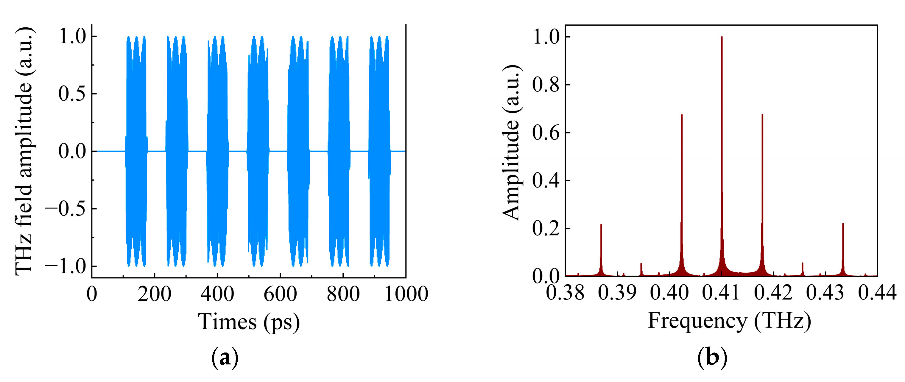
Following electro-optic modulation, the two modulated optical waves are coupled into a shared CPPLN waveguide, enabling the generation of a 0.41 THz difference-frequency signal. As depicted in Figure 4, the CDFG process begins with two input optical waves at frequencies ω 1 and ω 2 . Through sequential nonlinear interactions, these optical waves generate a series of progressively downshifted optical waves. At each cascaded stage, a frequency difference corresponding to the target THz signal is produced ( ω T = ω 1 ω 2 , ω T = ω 3 ω 4 ), with each new wave inheriting the THz frequency offset from its adjacent stages ( ω 3 = ω 2 ω T , ω 4 = ω 3 ω T , ω 5 = ω 4 ω T ).
In this process, photons from preceding stages interact to generate a new photon with a frequency reduced by ω T , enabling cumulative energy transfer across stages. This mechanism amplifies the energy of the target THz signal, ultimately yielding a high-energy THz signal with enhanced conversion efficiency. In contrast, conventional difference-frequency generation (DFG) schemes (First stage in Figure 4) rely on single-pass nonlinear conversion, theoretically limited by the Manley–Rowe efficiency limits [26].
The cascaded nonlinear interactions necessitate strict adherence to frequency and wave vector matching conditions for all participating optical fields during the parametric conversion process:
ω m + 1 = ω m ω T ,
ω T = ω m ω m + 1 ,
Δ k m = k m k m + 1 k T ,
where ω i and k i represent the frequency and wave vector of the cascaded optical waves, respectively. The subscript m denotes the cascaded optical sequence, ω T represents the frequency of the THz signal generated by the DFG process, Δ k represents the phase mismatch.
To compensate for the phase mismatch Δ k caused by dispersion, a fixed-period PPLN structure is conventionally employed to introduce a wave vector k Λ = Δ k , ensuring momentum conservation. As the cascaded order increases, the frequency of cascaded optical waves decreases while phase mismatch accumulates. Fixed-period poling structures cannot compensate for higher-order phase mismatch, leading to frequency upconversion and reduced THz signal conversion efficiency [16]. To address this issue, we employ a CPPLN structure with spatially changing poling periods, as shown in Figure 5a. This variation in poling period introduces a polarization inversion wave vector that sequentially compensates for the phase mismatch values across each stage of the CDFG process.
The calculation formula for the changing poling periods Λ N of CPPLN waveguide material is given by [27]:
Λ N z = c n z × N L + L × ω z × N L + n z × N L + 1 × ω z × N L + 1 + n T × ω T
where N represents the number of cascaded stages, and L denotes the maximum waveguide length. The changing poling periods Λ N introduces a quasi-phase-matching (QPM) wavevector k Λ , as illustrated in Equation (5):
k Λ z = 2 π Λ N z ,
Through chirped poling, CPPLN dynamically adjusts the QPM wavevector k Λ , enabling effective phase-mismatch compensation for Δ k m at each stage. This phase-mismatch compensation mechanism is one of the key advantages of CPPLN over fixed-period PPLN, especially for THz generation via the CDFG process.
Figure 5b shows the change of the CPPLN poling period along the waveguide length. The total length of the CPPLN waveguide is 6 mm. As the optical waves propagate through the waveguide, the poling period changes gradually from 225.42 μm at the waveguide position z = 0 mm to 225.18 μm at z = 6 mm.
In the CDFG process, the propagation of each cascaded optical wave within the waveguide is governed by the interaction between the electromagnetic field and the internal polarization field, as described by the coupled wave equations [26]:
d E T d z = α T 2 E T + j κ T E m E m + 1 * e j Δ k m z
d E m d z = α m 2 E m + j κ m E m 1 E T * e j Δ k m 1 z + E m + 1 E T e j Δ k m z
where E represents the electric field strength, α is the absorption coefficient, κ denotes the coupling coefficient between the optical wave and the waveguide, and z signifies the propagation distance of the optical wave within the waveguide. d E / d z indicates the spatial variation of the electric field E of frequency ω T or ω m passing through the nonlinear crystal. The first term on the right side of Equation (6) represents the material absorption of the THz wave at the frequency ω T , and the second term describes the nonlinear interaction between the optical waves at frequencies ω m and ω m + 1 , which generates the THz wave at frequency ω T in the CDFG process. The first term on the right side of Equation (7) signifies the material’s absorption of near-infrared waves at frequencies ω m and ω m + 1 during the cascaded process, while the second terms indicate the nonlinear interactions among the cascaded optical waves at frequencies ω m , ω m + 1 and ω T .
The calculation formulas for the coupling coefficients κ m and κ T are presented below [26]:
κ i = ω i d e f f c n i ,
where i represents T or m, which correspond to the THz and near-infrared waves, respectively. d e f f is the effective nonlinear coefficient of the crystal, n i denotes the refractive index at the corresponding optical frequency, and c is the speed of light in vacuum.
This work employs a magnesium oxide-doped chirped periodically poled lithium niobate (MgO:CPPLN) crystal for CDFG process. In such lithium niobate-based applications, temperature directly affects the terahertz absorption coefficient α T . In this work, the system is set to operate at 300 K, corresponding to room-temperature conditions. Previous studies have shown that decreasing the temperature can significantly reduce the terahertz absorption coefficient of lithium niobate [17]. This reduction would lower propagation losses within the CPPLN waveguide in the on-chip system, thereby enhancing the overall conversion efficiency.
Based on its Sellmeier dispersion equation [28], the refractive indices at 300 K are calculated as n m 2.14 for the near-infrared band and n T 5.20 for the 0.41 THz band [29,30]. The absorption coefficients at cascaded optical frequencies and the THz frequency are about 0 cm−1 and 16 cm−1 at 300 K [31,32]. The nonlinear coefficient of MgO:CPPLN at 0.41 THz is 336 pm/V [33].
The calculation formulas for the intensity of the generated THz wave and the energy conversion efficiency η are given by Equations (8) and (9) [26]:
I = 1 2 n c ε 0 | E T | 2 ,
η = n T | E T ω T , x | 2 + n m | E m ω m , 0 | 2 ,
where ε 0 is the vacuum permittivity.
In the ideal CDFG process, which disregards material absorption and coupling losses, the impact of the signal wave intensity ratio I ω 1 : I ω 2 on THz energy conversion efficiency is demonstrated in Figure 6a. The ideal energy conversion efficiency for THz wave generation peaks when I ω 1 : I ω 2 = 1 : 1 . Consequently, this on-chip system employs two equal-power optical waves modulated by the RMZMs for the CDFG process.
As shown in Figure 6b, in the CPPLN waveguide specifically designed for the CDFG process, the conversion efficiency increases with the waveguide length, reaching a maximum of 3.5% at 6 mm. This result demonstrates an improvement in conversion efficiency from 0.33% in conventional single-stage DFG approaches [26] and 1.8% in previous CDFG schemes based on 6 mm PPLN [34] to 3.5%, which confirms the cumulative advantage of the CPPLN-based CDFG scheme. For the on-chip THz modulation signal generation system, due to the existing losses in various components, the total conversion efficiency will be lower than 3.5%.

3. Results

Based on the RMZM and CPPLN, an on-chip THz modulation signal generation system is constructed. Its performance is evaluated through a simulation model, as illustrated in Figure 7. Initially, two optical waves with frequencies of 193.55 THz and 193.14 THz are passed through a polarization controller to adjust their polarization states. They are then amplified by an erbium-doped fiber amplifier (EDFA) before being injected into the on-chip system. Under the application of a modulation voltage signal V f , the RMZM modulators perform high-speed electro-optic modulation on the two input optical waves ( ω A and ω B ). The modulated signals ( ω 1 and ω 2 ) are subsequently coupled into a CPPLN waveguide via a Y-branch structure, enabling the generation of a 0.41 THz modulated signal ( ω T ) through the cascaded difference-frequency generation process. Finally, the system output is characterized using both an optical spectrum analyzer (OSA) and an electronic spectrum analyzer (ESA).
As shown in Figure 8a, the applied modulation voltage signal is an electrical pulse signal with an amplitude of 0.25 V. When the voltage changes from 0.25 V to 0 V, the racetrack resonator transitions from the zero-coupling state to the critical coupling state, causing the generated THz modulation signal to rapidly decrease to zero. Conversely, when the voltage changes from 0 V to 0.25 V, the racetrack resonator returns to the zero-coupling state, allowing the generated THz modulation signal to reach its peak intensity.
Figure 8b illustrates the temporal waveform of the generated THz electric field under 1 Gbit/s electrical modulation, clearly tracking the variation of the applied modulation voltage signal. Figure 8c shows the generated THz signal spectrum, which exhibits a distinct main peak and symmetrically distributed sidebands near 0.41 THz. The absence of significant spurious components or noise interference confirms high signal purity at the target terahertz frequency. During the simulation, the maximum output intensity reached 21.24 MW/cm2, while the minimum was 4.045 × 10−38 MW/cm2, resulting in a calculated modulation depth close to 100%.
During the CDFG process within the CPPLN waveguide, the propagation velocity of optical waves results in an additional delay in the generated THz modulation signal. At t 1 = L / ( c / n m ) = 42   ps , the modulated optical waves reach the waveguide exit, initiating the generation of a modulated THz signal. At a temperature of 300 K and an input optical intensity of 1000 MW/cm2 for both optical waves, the on-chip system experiences a delay of approximately 50 ps. This delay is due to the combined effects of various system components. Consequently, the on-chip system generates a modulated THz signal with a peak intensity of 21.24 MW/cm2, as shown in Figure 8d.
The maximum modulation signal generation rate v supported by the on-chip system is inversely proportional to the total response time T, which can be expressed as:
v = 1 T ,
T = t r e + t s ,
where t r e is the material response time, and t s is the stabilization time of the on-chip system.
Simulation results for the stabilization time of the on-chip system are shown in Figure 8d, indicating a stabilization time of 129 ps. Considering the fast response time (<1 ps) of the electro-optic effect in LN [35], the material response time is negligible; thus, the total response time of the on-chip system is approximately 129 ps. This stabilization time mainly includes the time required for the modulation process to stabilize and the build-up time of the THz cascaded difference-frequency generation process. Consequently, the maximum modulation signal generation rate supported by this on-chip system is calculated to be 7.75 Gbit/s according to Equation (11). Figure 9a illustrates the temporal waveform of the generated THz electric field at a 7.75 Gbit/s modulation rate. Figure 9b presents the generated THz signal spectrum at the same rate, exhibiting a pronounced peak at 0.41 THz. This result indicates that the on-chip system can support a maximum modulation signal generation rate of 7.75 Gbit/s. The simulation results indicate that the on-chip system supports a maximum modulation rate of 7.75 Gbit/s.
Compared to existing THz generation systems, the LN-based system offers distinct advantages for on-chip integration. While Si-based systems benefit from mature fabrication processes, they are constrained by high power consumption and limited modulation rates [17]. III–V semiconductor-based systems suffer from significant optical losses and integration challenges [36]. In contrast, the LN-based on-chip system combines a high electro-optic coefficient, strong nonlinear efficiency, and low optical loss, supporting high-speed modulation signal generation under low-voltage operating conditions. In addition, the current system is a single-frequency THz generation system, focused on the commonly used 0.41 THz signal in the THz communication window. By altering the input optical frequency and optimizing the structural parameters of the corresponding system components, the system can be adapted to generate signals at different frequency bands. Furthermore, the system architecture can be extended to support multi-frequency outputs by incorporating multi-wavelength inputs and parallel CPPLN waveguide arrays. This extension would enable broader spectral coverage and greater flexibility in THz modulation signal generation, addressing the demands of future multi-carrier THz communication systems. In practical applications, scaling the on-chip system to high-power operation may introduce challenges such as thermal effects caused by high input optical intensities. These thermal effects could affect the stability of the refractive index, the terahertz absorption coefficient, and phase-matching conditions. Additionally, achieving the designed poling periods of the CPPLN structure with high precision remains a fabrication challenge, particularly for long waveguides. These challenges can be addressed by incorporating additional thermal control modules and employing high-precision lithography techniques.

4. Conclusions

This study first proposes an on-chip THz modulation signal generation system that integrates RMZMs with a CPPLN waveguide. The on-chip system reduces the required modulation voltage and enhances THz signal intensity, while enabling high-speed THz modulation signal generation. Driven by two input optical waves at 193.55 THz and 193.14 THz, this on-chip system generates a modulated THz signal at 0.41 THz, with a 1 Gbit/s modulation rate and a 0.25 V modulation voltage. At an input optical wave intensity of 1000 MW/cm2 and a temperature of 300 K, the generated THz signal intensity reaches 21.24 MW/cm2. According to theoretical analysis, the maximum modulation signal generation rate supported by the on-chip system is 7.75 Gbit/s. In summary, the proposed on-chip system provides a compact and efficient solution for THz modulation signal generation. It shows strong potential for future applications in high-speed communication, real-time imaging, and integrated THz photonics.

Author Contributions

Conceptualization, H.Z., M.X. and M.M.; methodology, M.X. and H.Z.; software, H.Z.; validation, H.Z. and C.Z.; formal analysis, H.Z., M.X., M.M., C.Z., X.Z., W.M. and W.L.; investigation, H.Z. and M.X.; data curation, H.Z.; writing—original draft preparation, H.Z.; writing—review and editing, M.X., M.M., X.Z., W.M. and W.L.; supervision, M.X. and M.M. All authors have read and agreed to the published version of the manuscript.

Funding

This research was funded by the National Natural Science Foundation of China (61988102); the Program of GBA Branch of AIRCAS (E0Z2D10600).

Institutional Review Board Statement

Not applicable.

Informed Consent Statement

Not applicable.

Data Availability Statement

Data are available from the authors on request.

Conflicts of Interest

The authors declare no conflicts of interest.

References

  1. Jiang, Z.; Ding, G.; Luo, X.; Wang, S. Photoreconfigurable Metasurface for Independent Full-Space Control of Terahertz Waves. Sensors 2025, 25, 119. [Google Scholar] [CrossRef] [PubMed]
  2. Wang, C.; Lu, B.; Lin, C.; Chen, Q.; Miao, L.; Deng, X.; Zhang, J. 0.34-THz Wireless Link Based on High-Order Modulation for Future Wireless Local Area Network Applications. IEEE Trans. Terahertz Sci. Technol. 2014, 4, 75–85. [Google Scholar] [CrossRef]
  3. Tajima, T.; Song, H.-J.; Yaita, M. Compact THz LTCC Receiver Module for 300 GHz Wireless Communications. IEEE Microw. Wirel. Compon. Lett. 2016, 26, 291–293. [Google Scholar] [CrossRef]
  4. Teng, Y.L. 120 GHz On-chip Multi-mode Wideband Dielectric Resonator Antennas for THz Applications. Optoelectron. Lett. 2020, 16, 166–170. [Google Scholar] [CrossRef]
  5. Cheng, Y.Y.; Qiao, L.B.; Zhu, D.; Wang, Y.X.; Zhao, Z.R. Passive Polarimetric Imaging of Millimeter and Terahertz Waves for Personnel Security Screening. Opt. Lett. 2021, 46, 1233–1237. [Google Scholar] [CrossRef]
  6. Cassar, Q.; Caravera, S.; MacGrogan, G.; Bücher, T.; Hillger, P.; Pfeiffer, U.; Zimmer, T.; Guillet, J.-P.; Mounaix, P. Terahertz Refractive Index-Based Morphological Dilation for Breast Carcinoma Delineation. Sci. Rep. 2021, 11, 6457. [Google Scholar] [CrossRef]
  7. Ma, Z.T.; Geng, Z.X.; Fan, Z.Y.; Liu, J.; Chen, H.D. Modulators for Terahertz Communication: The Current State of the Art. Research 2019, 2019, 6482975. [Google Scholar] [CrossRef]
  8. Niessen, K.A.; Xu, M.; Markelz, A.G. Terahertz Optical Measurements of Correlated Motions with Possible Allosteric Function. Biophys. Rev. 2015, 7, 201–216. [Google Scholar] [CrossRef]
  9. Cheng, B.B.; Cui, Z.M.; Lu, B.; Qin, Y.L.; Liu, Q.; Chen, P.; He, Y.; Jiang, J.; He, X.Y.; Deng, X.J.; et al. 340-GHz 3-D Imaging Radar with 4Tx-16Rx MIMO Array. IEEE Trans. Terahertz Sci. Technol. 2018, 8, 509–519. [Google Scholar] [CrossRef]
  10. Kim, Y.; Zhang, Y.; Reck, T.J.; Nemchick, D.J.; Chattopadhyay, G.; Drouin, B.; Chang, M.C.F.; Tang, A. A 183-GHz InP/CMOS-Hybrid Heterodyne-Spectrometer for Spaceborne Atmospheric Remote Sensing. IEEE Trans. Terahertz Sci. Technol. 2019, 9, 313–334. [Google Scholar] [CrossRef]
  11. Ding, J.Q.; Shi, S.C.; Zhou, K.; Zhao, Y.; Liu, D.; Wu, W. WR-3 Band Quasi-Elliptical Waveguide Filters Using Higher Order Mode Resonances. IEEE Trans. Terahertz Sci. Technol. 2017, 7, 302–309. [Google Scholar] [CrossRef]
  12. Guo, C.; Shang, X.B.; Lancaster, M.J.; Xu, J.; Powell, J.; Wang, H.; Parow-Souchon, K.; Henry, M.; Viegas, C.; Alderman, B.; et al. A 290–310 GHz Single Sideband Mixer with Integrated Waveguide Filters. IEEE Trans. Terahertz Sci. Technol. 2018, 8, 446–454. [Google Scholar] [CrossRef]
  13. Li, Y.L.; Gao, W.; Guo, L.; Chen, Z.H.; Li, C.J.; Zhang, H.M.; Jiao, J.J.; An, B.W. Tunable Ultra-broadband Terahertz Perfect Absorber Based on Vanadium Oxide Metamaterial. Opt. Express 2021, 29, 41222–41233. [Google Scholar] [CrossRef]
  14. Yu, B.; Yang, J.; Song, Y.; Wang, Z.; Zhang, T.; Yan, B.; Xu, R. Terahertz Metamaterial Waveguide with I-Shaped Resonators for Phase and Absorption Modulation. Photonics 2023, 10, 816. [Google Scholar] [CrossRef]
  15. Xu, Z.; Ni, C.; Cheng, Y.; Dong, L.; Wu, L. Photo-Excited Metasurface for Tunable Terahertz Reflective Circular Polarization Conversion and Anomalous Beam Deflection at Two Frequencies Independently. Nanomaterials 2023, 13, 1846. [Google Scholar] [CrossRef]
  16. Iqbal, R.; Qureshi, U.U.R.; Jie, C.; Rahman, Z.U.; Jafar, N. Polarization and Incident Angle Independent Multifunctional and Multiband Tunable THz Metasurface Based on VO2. Nanomaterials 2024, 14, 1048. [Google Scholar] [CrossRef]
  17. Zhao, C.; Wang, D.; Lin, S.; Zhao, J.; Wang, Y.; Rong, L. Design Optimization of Silicon-Based Optically Excited Terahertz Wave Modulation. Photonics 2024, 11, 202. [Google Scholar] [CrossRef]
  18. Singh, P.; Sonkusale, S. High Speed Terahertz Modulator on the Chip Based on Tunable Terahertz Slot Waveguide. Sci. Rep. 2017, 7, 40933. [Google Scholar] [CrossRef] [PubMed]
  19. Zhang, R.; Cao, Y.; Li, X.; Yang, X.; Li, S.; Lang, L. On-Chip Terahertz Amplitude Modulator Unit in Series Configuration Design. Opt. Commun. 2025, 579, 131546. [Google Scholar] [CrossRef]
  20. Delfanazari, K. On-Chip Coherent Terahertz Emitters with Gigahertz Modulation. Nat. Photonics. 2024, 18, 214–215. [Google Scholar] [CrossRef]
  21. Ding, K.; Liang, S.; Zou, L.; Gong, S.; Zhang, Y. Terahertz High-Speed On-Chip Modulator Based on SRR. In Proceedings of the 24th International Vacuum Electronics Conference (IVEC), Chengdu, China, 25–28 April 2023. [Google Scholar] [CrossRef]
  22. Yu, X.; Gan, R.F.; Chen, K.X.; Chen, G.X.; Ruan, Z.L.; Zhang, J.W.; Liu, J.; Dai, D.X.; Guo, C.J.; Liu, L. Breaking the Bandwidth Limit of a High-Quality-Factor Ring Modulator Based on Thin-Film Lithium Niobate. Optica 2022, 9, 1131–1137. [Google Scholar] [CrossRef]
  23. Wang, C.; Zhang, M.; Chen, X.; Bertrand, M.; Shams-Ansari, A.; Chandrasekhar, S.; Winzer, P.; Lončar, M. Integrated Lithium Niobate Electro-Optic Modulators Operating at CMOS-Compatible Voltages. Nature 2018, 562, 101–104. [Google Scholar] [CrossRef] [PubMed]
  24. Chen, G.X.; Chen, K.X.; Gan, R.F.; Ruan, Z.L.; Wang, Z.; Huang, P.C.; Lu, C.; Lau, A.P.T.; Dai, D.X.; Guo, C.J.; et al. High Performance Thin-Film Lithium Niobate Modulator on a Silicon Substrate Using Periodic Capacitively Loaded Traveling-Wave Electrode. APL Photonics 2022, 7, 2. [Google Scholar] [CrossRef]
  25. Ma, X.F.; Wang, N.Y.; Cao, R.Z.; Sheng, C.; Zhu, S.; Liu, H. Optical to Terahertz Frequency Conversion Using Near Zero-Index Nonlinear Hybrid Waveguides. Opt. Contin. 2024, 3, 682–690. [Google Scholar] [CrossRef]
  26. Li, Z.; Sun, X.Q.; Zhang, H.T.; Li, Y.J.; Yuan, B.; Jiao, B.Z.; Zhao, J.; Tan, L.; Bing, P.; Wang, Z.; et al. High-Efficiency Terahertz Wave Generation in Aperiodically Poled Lithium Niobate by Cascaded Difference Frequency Generation. J. Opt. Soc. Am. B 2020, 37, 2416–2422. [Google Scholar] [CrossRef]
  27. Li, Z.; Yan, Q.; Chen, X.; Bing, P.; Yuan, S.; Zhong, K.; Yao, J. Investigation of Efficient Terahertz Wave Generation by Coupled Cascade Difference Frequency Generation. Chin. J. Lasers 2023, 50, 0614001. [Google Scholar] [CrossRef]
  28. Kato, K.; Takaoka, E. Sellmeier and Thermo-Optic Dispersion Formulas for KTP. Appl. Opt. 2002, 41, 5040–5044. [Google Scholar] [CrossRef]
  29. Zelmon, D.E.; Small, D.L.; Jundt, D. Infrared Corrected Sellmeier Coefficients for Congruently Grown Lithium Niobate and 5 mol.% Magnesium Oxide–Doped Lithium Niobate. J. Opt. Soc. Am. B 1997, 14, 3319–3322. [Google Scholar] [CrossRef]
  30. Kiessling, J.; Buse, K.; Breunig, I. Temperature-Dependent Sellmeier Equation in the MIR for the Extraordinary Refractive Index of 5% MgO Doped Congruent LiNbO3. Appl. Phys. B 2007, 86, 111–115. [Google Scholar] [CrossRef]
  31. Ravi, K.; Schimpf, D.N.; Kärtner, F.X. Pulse Sequences for Efficient Multi-Cycle Terahertz Generation in Periodically Poled Lithium Niobate. Opt. Express 2016, 24, 25582–25607. [Google Scholar] [CrossRef]
  32. Liu, P.; Xu, D.; Yu, H.; Zhang, H.; Li, Z.; Zhong, K.; Wang, Y.; Yao, J. Coupled-Mode Theory for Cherenkov-Type Guided-Wave Terahertz Generation via Cascaded Difference Frequency Generation. J. Light. Technol. 2013, 31, 2508–2514. [Google Scholar] [CrossRef]
  33. Pálfalvi, L.; Hebling, J.; Kuhl, J.; Péter, Á.; Polgár, K. Temperature Dependence of the Absorption and Refraction of Mg-doped Congruent and Stoichiometric LiNbO3 in the THz Range. J. Appl. Phys. 2005, 97, 123505. [Google Scholar] [CrossRef]
  34. Ravi, K.; Hemmer, M.; Cirmi, G.; Reichert, F.; Schimpf, D.; Mücke, O.; Kärtner, F. Cascaded parametric amplification for highly efficient terahertz generation. Opt. Lett. 2016, 41, 3806–3809. [Google Scholar] [CrossRef] [PubMed]
  35. Wang, T.J.; Peng, G.L.; Chan, M.Y.; Chen, C.H. On-Chip Optical Microresonators with High Electro-Optic Tuning Efficiency. J. Light. Technol. 2020, 38, 1851–1857. [Google Scholar] [CrossRef]
  36. Zhang, Y.; Ding, K.; Zeng, H.; Kou, W.; Zhou, T.; Zhou, H.; Gong, S.; Zhang, T.; Wang, L.; Liang, S.; et al. Ultrafast modulation of terahertz waves using on-chip dual-layer near-field coupling. Opt. Lett. 2022, 9, 1268–1275. [Google Scholar] [CrossRef]
Figure 1. (a) On-chip THz modulation signal generation system. (b) Cross-sectional geometry of the RMZM.
Photonics 12 00490 g001
Figure 2. (a) RMZM structure and electrode position. (b) Schematic of critical coupling state. (c) Schematic of zero coupling state.
Photonics 12 00490 g002
Figure 3. Transmission spectra near the 1550 nm resonant wavelength at different voltages.
Photonics 12 00490 g003
Figure 4. Principle of CDFG.
Photonics 12 00490 g004
Figure 5. (a) CDFG scheme based on CPPLN. (b) The change of the CPPLN poling period along the waveguide length.
Photonics 12 00490 g005
Figure 6. (a) Impact of the ratio of input signal wave intensity on ideal energy conversion efficiency in the CDFG process. (b) Conversion efficiency as a function of propagation distance along the waveguide.
Photonics 12 00490 g006
Figure 7. Simulation of the on-chip terahertz modulation signal generation system based on RMZM and CPPLN.
Photonics 12 00490 g007
Figure 8. (a) Applied modulation voltage signal at a rate of 1 Gbit/s. (b) Temporal waveform of the generated THz electric field under a modulation voltage signal of 1 Gbit/s. (c) Generated THz signal spectrum under a modulation voltage signal of 1 Gbit/s. (d) Transient response curve of the on-chip system.
Photonics 12 00490 g008
Figure 9. (a) Temporal waveform of the generated THz electric field under a modulation voltage signal of 7.75 Gbit/s. (b) Generated THz signal spectrum under a modulation voltage signal of 7.75 Gbit/s.
Photonics 12 00490 g009
Disclaimer/Publisher’s Note: The statements, opinions and data contained in all publications are solely those of the individual author(s) and contributor(s) and not of MDPI and/or the editor(s). MDPI and/or the editor(s) disclaim responsibility for any injury to people or property resulting from any ideas, methods, instructions or products referred to in the content.

