Review

Hybrid Photonic Integrated Circuits for Wireless Transceivers

by
Tianwen Qian
1,*,
Ben Schuler
1,
Y. Durvasa Gupta
1,
Milan Deumer
1,
Efstathios Andrianopoulos
2,
Nikolaos K. Lyras
3,
Martin Kresse
1,
Madeleine Weigel
1,
Jakob Reck
1,
Klara Mihov
1,
Philipp Winklhofer
1,
Csongor Keuer
1,
Laurids von Emden
1,
Marcel Amberg
1,
Crispin Zawadzki
1,
Moritz Kleinert
1,
Simon Nellen
1,
Davide de Felipe
1,
Hercules Avramopoulos
2,
Robert B. Kohlhaas
1,
Norbert Keil
1 and
Martin Schell
1,4
add Show full author list remove Hide full author list
1
Fraunhofer Institute for Telecommunications, Heinrich-Hertz-Institute, HHI, Einsteinufer 37, 10587 Berlin, Germany
2
Photonics Communications Research Laboratory, National Technical University of Athens, 15572 Athens, Greece
3
Optoelectronics Section, European Space Agency, Estec, Keplerlaan 1, 2201 AZ Noordwijk, The Netherlands
4
Institute of Solid-State Physics, Technische Universität Berlin, Straße des 17. Juni 135, 10623 Berlin, Germany
*
Author to whom correspondence should be addressed.
Photonics 2025, 12(4), 371; https://doi.org/10.3390/photonics12040371
Submission received: 15 March 2025 / Revised: 5 April 2025 / Accepted: 9 April 2025 / Published: 12 April 2025
(This article belongs to the Special Issue Advanced Technologies in Optical Wireless Communications)

Abstract

:
Recent advancements in hybrid photonic integrated circuits (PICs) for wireless communications are reviewed, with a focus on innovations developed at Fraunhofer HHI. This work leverages hybrid integration technology, which combines indium phosphide (InP) active elements, silicon nitride (Si3N4) low-loss waveguides, and high-efficient thermal-optical tunable polymers with micro-optical functions to achieve fully integrated wireless transceivers. Key contributions include (1) On-chip optical injection locking for generating phase-locked optical beat notes at 45 GHz, enabled by cascaded InP phase modulators and hybrid InP/polymer tunable lasers with a 3.8 GHz locking range. (2) Waveguide-integrated THz emitters and receivers, featuring photoconductive antennas (PCAs) with a 22× improved photoresponse compared to top-illuminated designs, alongside scalable 1 × 4 PIN-PD and PCA arrays for enhanced power and directivity. (3) Beam steering at 300 GHz using a polymer-based optical phased array (OPA) integrated with an InP antenna array, achieving continuous steering across 20° and a 10.6 dB increase in output power. (4) Demonstration of fully integrated hybrid wireless transceiver PICs combining InP, Si3N4, and polymer material platforms, validated through key component characterization, on-chip optical frequency comb generation, and coherent beat note generation at 45 GHz. These advancements result in compact form factors, reduced power consumption, and enhanced scalability, positioning PICs as an enabling technology for future high-speed wireless networks.

1. Introduction

The rapid growth of global data traffic, driven by emerging technologies such as 5G/6G networks, the Internet of Things (IoT), and artificial intelligence (AI), has created an unprecedented demand for high-speed, high-capacity wireless communication systems [1,2]. Traditional radio-frequency (RF) technologies, while widely deployed, face fundamental limitations in bandwidth, energy efficiency, and signal integrity, particularly as we approach the millimeter-wave (mmWave) terahertz (THz) regime [3,4,5]. In this context, photonic technologies offer significant advantages [6]. By leveraging the ultra-wide bandwidth capabilities of mature optical fiber communication technology, photonic systems enable the generation and modulation of signals in the optical domain, which can be efficiently converted into electrical signals up to THz range through photomixing [7,8,9].
Early demonstrations of photonic wireless systems relied on discrete components, such as fiber-coupled lasers, external Mach–Zehnder modulators (MZMs), and free-space optical setups. They achieved impressive data rates, for example, up to 100 Gbit/s in the 100 GHz band [10], but were limited by their large footprint, high power consumption, and susceptibility to alignment issues [3,5].
Recent advancements in photonic integration have enabled the development of chip-scale systems. Here, silicon photonics (SiPh) has gained significant attention due to its compatibility with CMOS processes, which enables low-cost and high-volume production of integrated modulators and detectors [11,12]. However, it faces challenges such as the lack of efficient on-chip light sources and the lack of volumes required for CMOS-style processes. This limitation has spurred the development of hybrid integration strategies, combining silicon with III-V materials like indium phosphide (InP) to incorporate high-performance lasers and amplifiers [13,14].
On the other hand, InP excels in monolithic integration of active components, such as lasers, amplifiers, and high-speed modulators, making them highly suitable for compact and efficient photonic transceivers [15,16]. However, InP is limited in passive component performance, and for that, low-loss materials like silicon nitride (Si3N4) [17,18] and polymers [19,20] are better suited. Si3N4 is renowned for its ultra-low optical loss [17]. Polymer material platforms, such as PolyBoard [19], offer low-loss waveguides and feature versatile micro-optical benches that can integrate bulk optic functionalities onto the chip. Its various refractive index contract waveguide system enables seamless co-integration with other materials. Additionally, lithium niobate (LiNbO3) has gained attention for its exceptional electro-optic properties, enabling high-speed modulators with low power consumption [21,22,23,24]. Furthermore, plasmonics-enabled modulators have demonstrated ultra-high frequency responses, reaching the sub-terahertz range [25].
Fraunhofer HHI has been developing solutions that provide compact form factors, reduced power consumption, and enhanced scalability for such photonic integrated circuits (PICs), for example, using the PolyBoard platform to integrate active components such as lasers, modulators, and photodiodes, as well as nonlinear and nonreciprocal bulk optic functionalities through hybrid integration [26,27,28,29].
In this work, we present a new generation of PICs for wireless communications, involving the InP, Si3N4, and polymer material platforms. This integration scheme offers fully integrated PICs with building blocks such as tunable lasers, on-chip optical isolators, optical phased arrays (OPAs), modulators, semiconductor optical amplifiers (SOAs), positive-intrinsic-negative photodiodes (PIN-PDs), and waveguide-integrated photoconductive antennas (PCA). The generation of low-phase-noise wireless carriers through the on-chip frequency comb generation and injection locking yields a photonic engine for microwave signal generation. Moreover, the combination of an OPA and InP PIN-PD-based antenna array yields a directional and reconfigurable antenna array for wireless communication.

2. Key Photonic Subsystems for Wireless Transceiver PICs

Hybrid integration takes the approach of using the advantage of each material platform. Table 1 lists the photonic functionalities offered on the material platforms that are going to be considered in this work for the implementation of the photonic wireless transceivers. The hybrid approach allows for good yield management even for complex photonic integrated circuits, as only known good dies from each platform are used for the hybrid integration. The key photonic subsystems that are going to be discussed are listed below:
  • Optical injection-locked laser source for wireless communications
  • Photonic THz emitter and receiver
  • Beam steering with OPA and optical beam-forming network (OBFN)

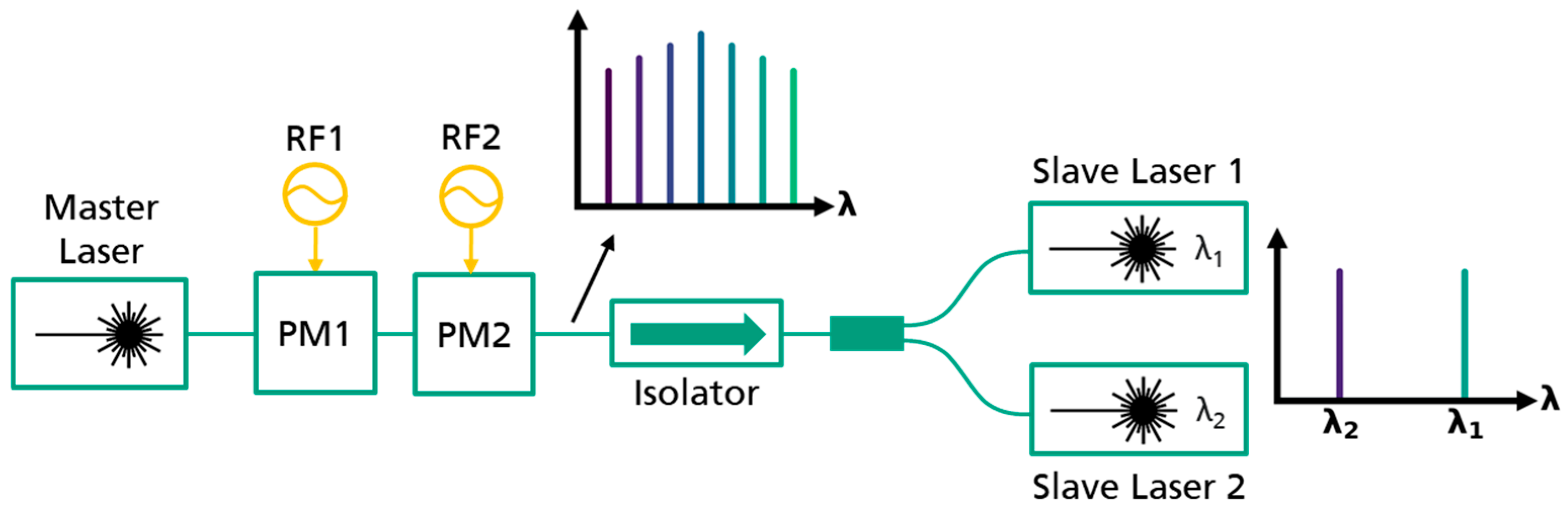
2.1. Optical Injection-Locked Laser Source for Wireless Communications

Figure 1 illustrates the schematic for generating phase-locked optical signals, a critical step in generating a low-phase-noise mmWave and THz signal by means of photomixing [9]. This process employs the optical injection locking technique [30,31], which ensures the phase coherence and stability in the generated signals. The optical signal from the narrow linewidth master laser passes through two cascaded phase modulators (PMs). These PMs are independently controlled by sinusoidal RF signals, enabling the generation of an optical frequency comb (OFC). The generated OFC is then used to injection-lock the two slave lasers, producing phase-locked optical signals. The optical isolator is incorporated to prevent feedback into the master laser. The required photonic building blocks for this subsystem are discussed in detail below.

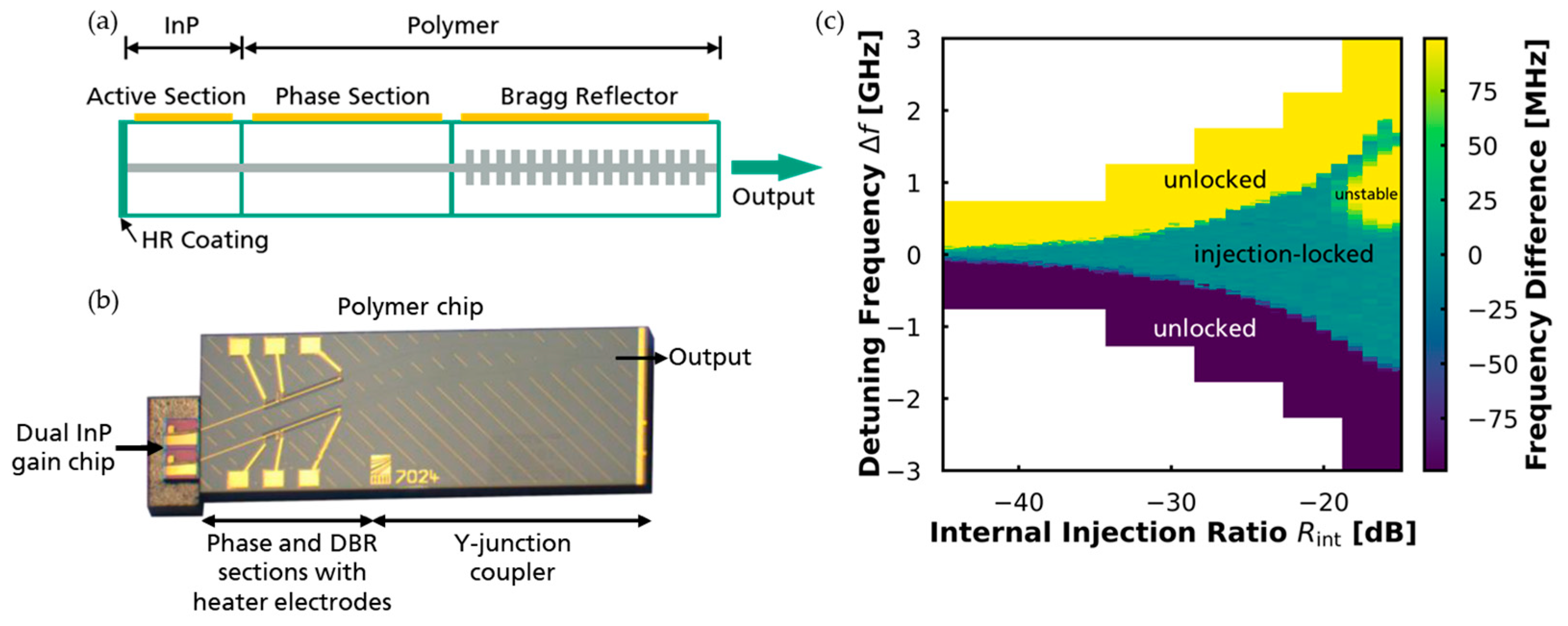
2.1.1. InP/Polymer Tunable Laser

Hybrid PIC-based external cavity diode lasers (ECDLs) have emerged as reliable, tunable, narrow linewidth laser sources. PICs with Vernier microring resonators (MRR) [32], distributed Bragg reflectors [33,34,35], Sagnac loop reflectors (SLRs) [36], and Mach–Zehnder interferometers [37] have been fabricated on silicon (Si) [37], silicon dioxide (SiO2) [38], Si3N4 [32,34,35,39,40], polymers [33,41], and other materials [42,43].
Fraunhofer HHI’s PolyBoard and InP foundry platforms offer hybrid InP/polymer tunable distributed Bragg reflector (DBR) lasers, operating in the telecom window with a center wavelength of approximately 1550 nm. These lasers offer a tuning range exceeding 20 nm, a narrow linewidth of 185 kHz, and optical power levels of up to 40 mW [41]. The cross-sectional schematic of the InP/polymer tunable laser is shown in Figure 2a. The DBR laser cavity consists of an InP active element serving as the gain medium and a polymer-based section incorporating a thermo-optically tunable phase section and Bragg grating. The left facet of the InP active section is high-reflection (HR) coated against air, while the right facet is anti-reflection (AR) coated against polymers.
Compared to the other types of ECDLs, this design offers a significant advantage: a large mode-hop-free tuning range of up to 1.5 THz (12 nm) [44], while other types of ECDLs are still limited in the hundreds of GHz range [45,46]. This could enable seamless tuning of photonic-generated wireless carriers targeting mmWave and THz applications. Additionally, its compact footprint allows for easy scalability with arrays of InP gain chips; an example of a dual hybrid InP/polymer DBR laser is shown in Figure 2b. Furthermore, the PolyBoard platform supports additional hybrid integration features, such as on-chip optical isolators. Therefore, we chose this hybrid InP/polymer tunable DBR laser to explore the implementation of optical injection locking systems to generate phase-locked optical signals.
The characterization of hybrid DBR lasers in a master–slave configuration has been experimentally verified to achieve stable injection locking. By defining the detuning frequency Δf as the difference frequency between the master laser and slave laser, and the internal injection ratio R i n t = P i n j e c t i o n P s l a v e as the ratio of the injected power to the slave laser power, the locking behavior is charted in Figure 2c. A locking range of 0.2 GHz to 3.8 GHz was observed. Under stable injection-locked conditions, the slave laser follows the frequency of the master laser, and the measured frequency difference is less than 20 MHz. The boundaries of the locking range are visible as sharp transitions. Outside the locking range, the frequency difference increases significantly. For a large internal injection ratio R i n t , a small unstable region is observed within the locking range, corresponding to the undamped relaxation oscillations [47]. In this region, the frequency deviation increases abruptly, as the relaxation oscillations dominate the power distribution and alter the optical frequency.

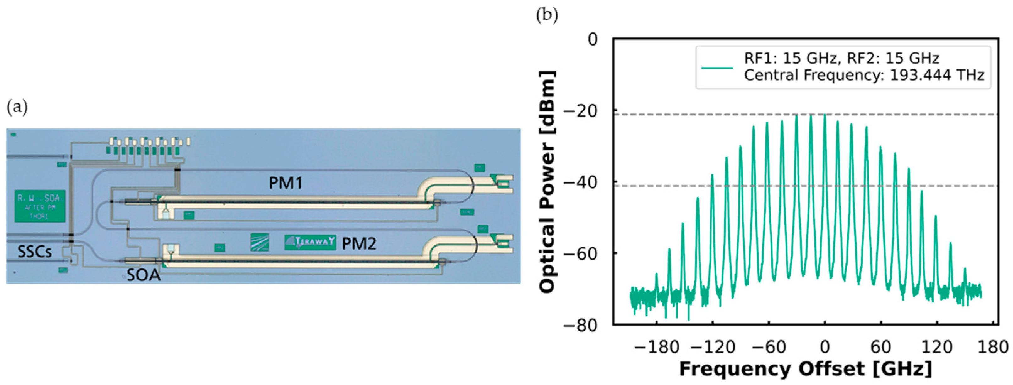
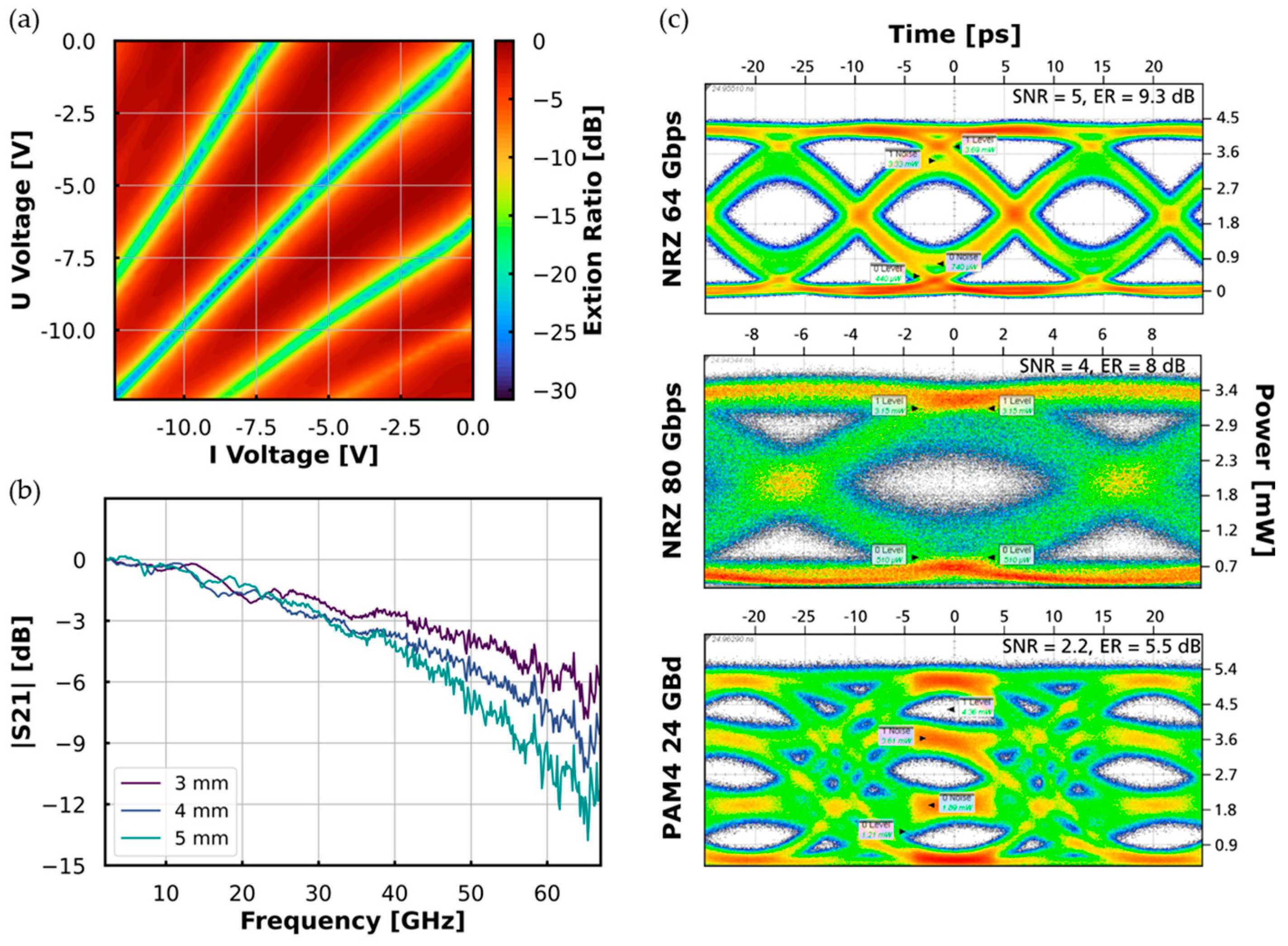
2.1.2. InP Electro-Optic Modulator

There are several different ways of generating OFCs using integrated photonic approaches, e.g., Kerr soliton combs in high-Q microresonators [48,49], which offer ultra-low phase noise and broad bandwidth but require precise control of pump power and dispersion, mode-locked lasers [48,50], which provide excellent coherence and high repetition rates but have limited tunability due to fixed cavity designs and gain-switched laser combs [51], which are simple and cost-effective with moderate tunability but suffer from spectral flatness and phase noise limitations.
Here, we chose two cascaded InP-based electro-optic modulators, which are modulated with sinusoidal RF driving currents and thus generate an OFC [52,53,54]. This offers a highly flexible and frequency-tunable approach, making them particularly suitable for microwave photonics applications. E/O combs can be precisely controlled via microwave driving signals, enabling tailored comb spacing and phase coherence, which are critical for generating high-quality microwave signals.
The generic InP foundry integration platform at HHI provides high-bandwidth traveling-wave modulators based on the quantum-confined Stark effect (QCSE) [52,55]. Additionally, SOAs can be integrated directly after the phase modulator to enhance the power of each comb line. Figure 3a shows the InP chip with two cascaded phase modulators followed by a SOA, and an example of a generated OFC is shown in Figure 3b.
Based on the traveling wave electrode structure, high-speed MZMs have been optimized and offered as a standard building block on the InP foundry platform [15]. Figure 4 shows their typical DC and RF characteristics.
Figure 4a presents the extinction ratio (ER) map of a MZM with a 5 mm long active section for a TE-polarized optical input at 1550 nm. U and I represent the voltages applied across the arms of the electrodes. The half-wave voltage (Vπ) is 1.4 V at a bias voltage of −10 V, corresponding to a Vπ · L value of 0.7 V · cm. The measured maximum ER is approximately 31 dB. Figure 4b illustrates the small-signal RF response of the MZMs with active lengths of 3 mm, 4 mm, and 5 mm, with corresponding 3 dB bandwidths of 42 GHz, 34 GHz, and 32 GHz, respectively. Figure 4c depicts the large-signal characterization of the MZM with a 5 mm-long active section for 64 Gbps NRZ, 80 Gbps NRZ, and 24 GBd PAM4. The extinction ratios for these modulation formats are 9.3 dB, 8 dB, and 5.5 dB, respectively. For more details on the characterization, please refer to [15].

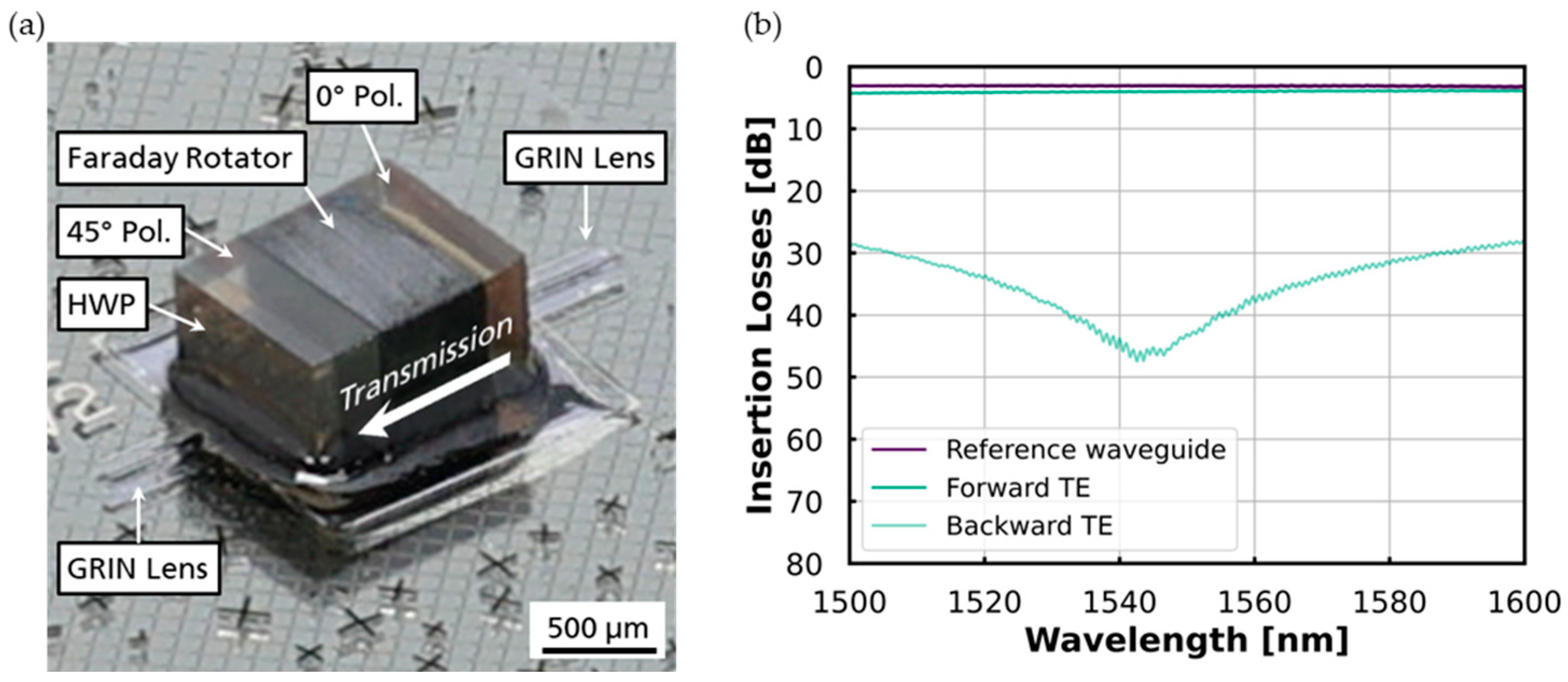
2.1.3. Optical Isolators

Optical isolators are essential in the injection locking technique to prevent feedback from the slave lasers, ensuring stable operation of the system. The PolyBoard platform’s micro-optical bench allows for the integration of bulk nonreciprocal optical elements directly into a photonic chip. The isolator incorporates a Faraday rotator sandwiched between a 0° polarization filter and a 45° polarization filter, followed by a 22.5° half-wave plate (HWP) to ensure TE polarization in the forward transmission direction. The optical coupling between the waveguide and free space is optimized through gradient-index (GRIN) lenses, which can be placed in the etched U-groove structures on the PolyBoard. Figure 5a shows a close-up picture of the integrated optical isolator. Over 30 dB isolation across the C-band with an excess loss below 1.5 dB can be achieved, as shown in Figure 5b [28,29,56].

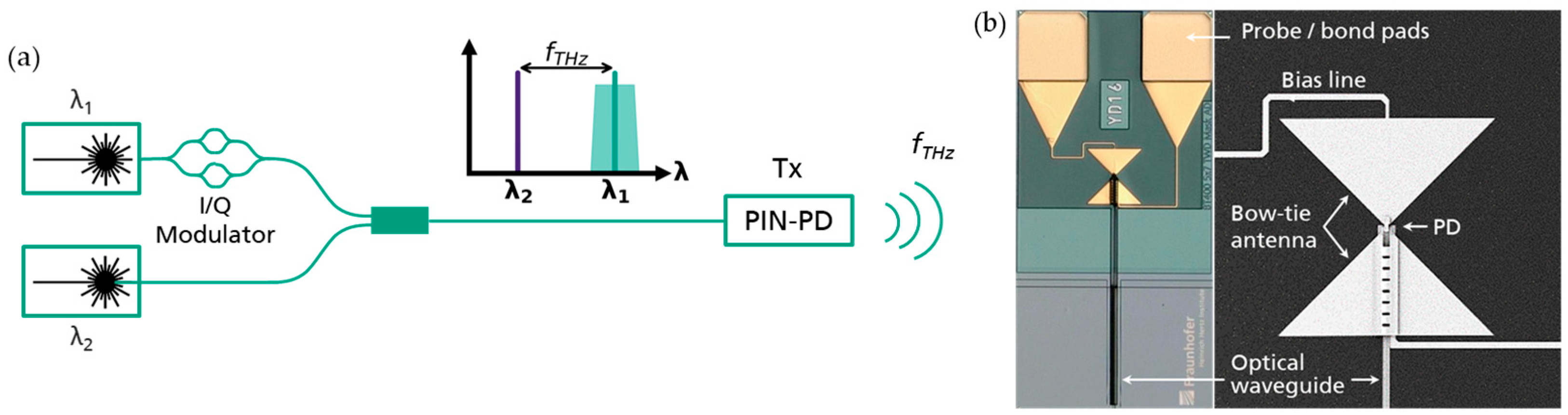
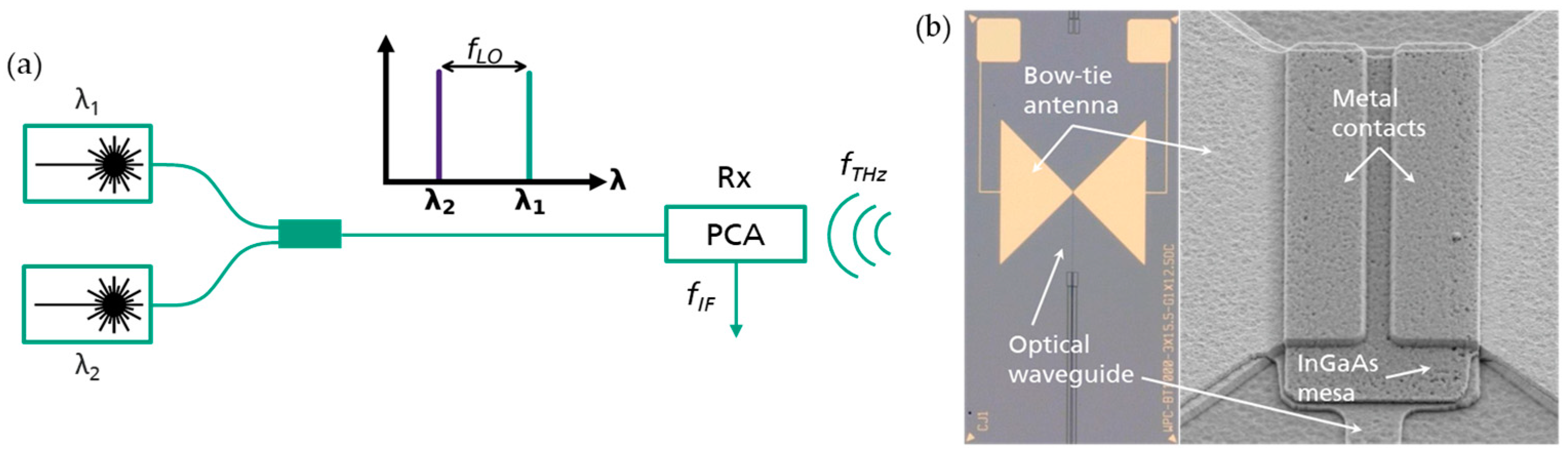
2.2. Photonic THz Emitter and Receiver

By superimposing the two phase-locked optical signals, a stable optical beat note is generated, which is then converted into a THz signal using a photomixer. On the receiver side, the beat note serves as a local oscillator to down-convert the incident THz signal to an intermediate frequency for electronic acquisition. For the transmitter (Tx), commonly PIN-PDs or uni-traveling-carrier (UTC) PDs are employed as photomixers [57,58,59,60], while photoconductive antennas (PCAs) are better suited for the receiver (Rx) [61,62,63].
For our transmitter, waveguide-integrated PIN-PDs, based on mature processes originally developed for fiber-optic communication systems, have demonstrated coherent links with data rates of up to 160 Gbit/s and well-defined radiation patterns [64,65]. For coherent communication, an InP in-phase/quadrature (I/Q) modulator imprints the data onto one of the optical signals before superposition, as shown in Figure 6. An I/Q modulator is typically constructed using two parallel MZMs. All these building blocks, i.e., lasers, MZMs, and PDs, are readily available on the InP platform.
On the receiver side, as shown in Figure 7, the antenna receives the incident THz signal, inducing a voltage variation at frequency f T H z across the photoconductor located at the antenna’s feed point. At the same time, the optical beat signal fed into the photoconductor acts as a local oscillator (LO) with the difference frequency of the two phase-locked laser signals f L O , which modulates the conductance of the photoconductor. This oscillating conductance in the feeding point of the antenna leads to a down-conversion of the THz signal to an intermediate frequency (IF) f I F = f T H z f L O that can be measured with conventional electronics. Note that photonic integration requires waveguide-integrated PCAs and not traditional top-illuminated designs [66]. By integrating the PCA with optical waveguides, evanescent coupling enhances the light coupling efficiency into the photoconductive material. Unlike top-illuminated PCAs, which suffer from reflections at the air-semiconductor interface, waveguide-integrated PCAs minimize these losses by coupling light from below, resulting in improved optical absorption and higher output signal strength. Recent developments in waveguide-integrated PCAs have demonstrated up to 22-fold improvement in photoresponse compared to state-of-the-art top-illuminated designs [66], enabling flexible integration of THz receivers into photonic integrated circuits.

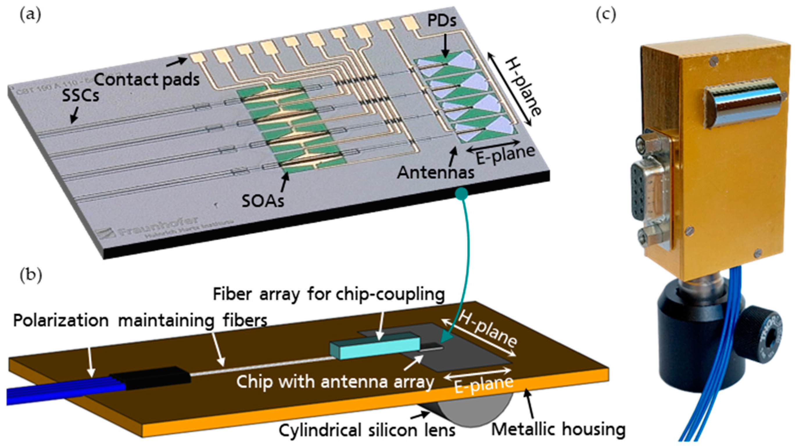
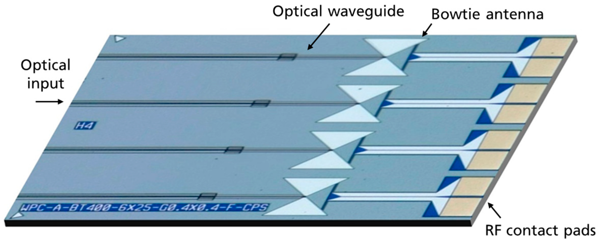
Scaling-Up with Antenna Arrays

To address the limitations of emitted power and antenna directivity [59,65,68,69,70] in mmWave and THz communication systems, arrays of antennas are implemented. The antenna pitch must be smaller than the targeting wavelength to achieve beam steering capability, necessitating waveguide-integrated designs to enable the required compact spacing, which discrete components cannot provide. This approach enables scalable and high-performance THz transmitters and receivers. A 1 × 4 THz emitter array based on PIN-PDs integrated with SOA [68] and a 1 × 4 THz receiver array based on PCAs are depicted in Figure 8 and Figure 9, respectively. SSCs are included on the chip facet to facilitate the coupling towards standard fiber array or other chip platforms.

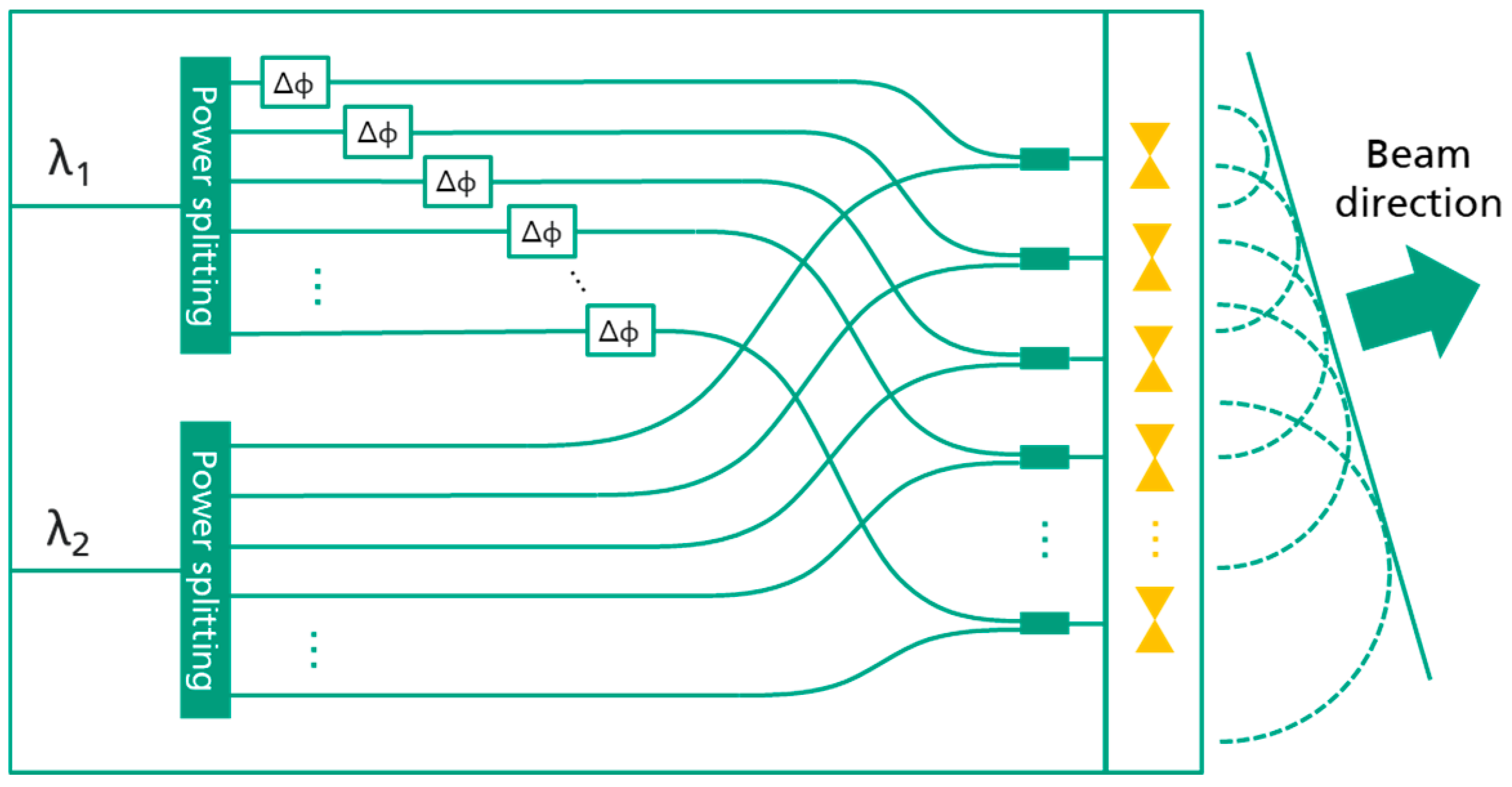
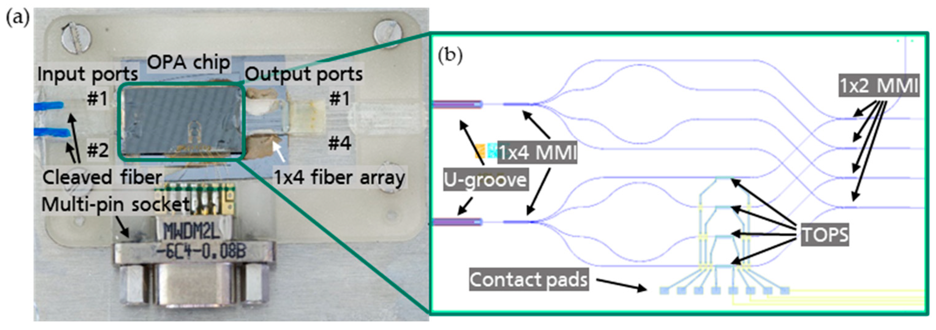
2.3. Beam Steering with OPA and OBFN

Beam steering can be achieved by integrating OPAs with antenna arrays, where the phase of each individual antenna element is precisely controlled [71]. Figure 10 illustrates a schematic design of such an OPA, which utilizes two phase-locked optical signals as inputs. Power-splitting elements, such as multimode interferometers (MMIs), distribute the signals to the desired number of antennas. To maintain phase correlation between the two signals, the optical path lengths must be identical, necessitating low-loss waveguide routing. By introducing phase shifting in one of the optical signals, a wide steering angle can be achieved with tuning speeds in the MHz and GHz range [69,72,73].
The PolyBoard platform offers waveguide propagation loss down to 0.8 dB/cm [19] and also includes building blocks, such as efficient thermo-optical phase shifters with low crosstalk. These phase shifters leverage the platform’s high thermo-optical coefficient and low thermal conductivity, outperforming other photonic integration platforms [68].
Figure 11 shows a packaged 1 × 4 OPA array based on the PolyBoard platform. By controlling it in conjunction with the 1 × 4 THz emitter array shown in Figure 8, an increased output power of 10.6 dB, higher directivity, and continuous beam steering across 20° at 300 GHz have been successfully demonstrated in [68]. Note that the use of a silicon lens imposes a limitation on the steering angle due to total internal reflection within the silicon. To achieve wider steering angles, dielectric rod waveguide (DRW) antennas have been explored, demonstrating compatibility with the hybrid integration approach [74,75]. Alternative methods, such as metasurface-based beam steering, offer the potential for compact designs with wide-angle steering capabilities; however, many of these approaches remain largely theoretical [76,77]. For a larger antenna array, to overcome the beam squint effect [78,79,80], using an optical Blass matrix-based OBFN to introduce time delay into the signal is also possible with the platform solution [81,82,83].

3. Towards Full-Photonic Wireless Transmitter and Receiver PICs

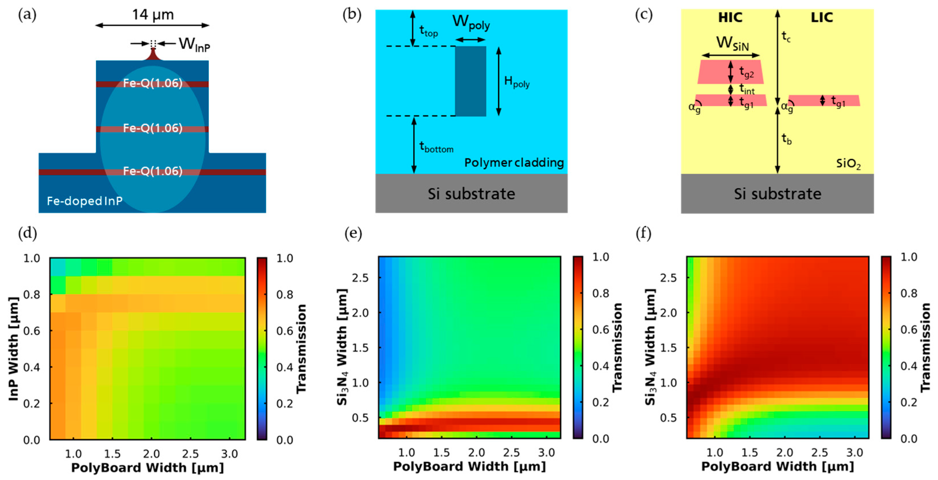
3.1. Optical Interfacing Between PIC Technologies

Moreover, integrating the aforementioned photonic building blocks into the hybrid PIC requires efficient coupling between each platform. Numerical simulations were performed using ANSYS Lumerical MODE (version: 2024 R1), optimizing the waveguide width for each material platform to achieve optimal mode overlap and maximize mode-field diameters, thereby enhancing coupling tolerance. Table 2 provides an overview of the waveguide properties for the different material platforms used in the transceiver PICs. Parameters such as neff are the effective refractive index; MFDx,y are mode-filed diameters where the optical power has dropped to 1/e2 of the maximum intensity. The waveguide width varied in the simulation is listed, as well as the simulated coupling loss towards the PolyBoard. Figure 12 shows the schematic of the waveguide cross-section of (a) InP SSC, (b) PolyBoard, and (c) Si3N4 [17], and their corresponding simulation results.
The SSC on the InP platform is implemented by inverse-tapering the InP Q(1.06) waveguide width, WInP, enabling evanescent coupling to the substrate mode within the so-called dilute waveguide [16]. This waveguide is formed by three layers of Fe-doped passive InP Q(1.06) waveguides. The PolyBoard taper is achieved through an inverse taper by varying the waveguide width, Wpoly. A refractive index contrast of Δn = 0.03 (ncore = 1.48, ncladding = 1.45) is used, while the waveguide height, Hpoly, is fixed at 3.2 µm. For the Si3N4 platform, the asymmetric double-stripe (ADS) waveguide offers the natural transition between high-index-contract (HIC) and low-index-contract (LIC) waveguides, combining small bending radii with ultra-low-loss propagation [17]. In this case, the width of the Si3N4 waveguide, WSiN, is varied to optimize coupling with the PolyBoard waveguide.
Figure 12d shows that the highest transmission between InP and the polymer occurs at a polymer waveguide width of 0.8 µm, corresponding to a coupling loss of 1.3 dB. Additionally, the transmission remains nearly constant for InP widths ranging from 0.1 µm to 0.65 µm, ensuring robustness against width variations caused by etching or lithography. An InP waveguide width of 0.25 µm is chosen, allowing for an etching tolerance of ±100 nm. For both Si3N4 HIC and LIC waveguides, optimal coupling is achieved with a 0.8 µm polymer waveguide, resulting in a coupling loss of 0.1 dB. Although simulations suggest additional viable options, we selected the 0.8 µm polymer waveguide for interfacing with InP and Si3N4 waveguides to maintain design simplicity.

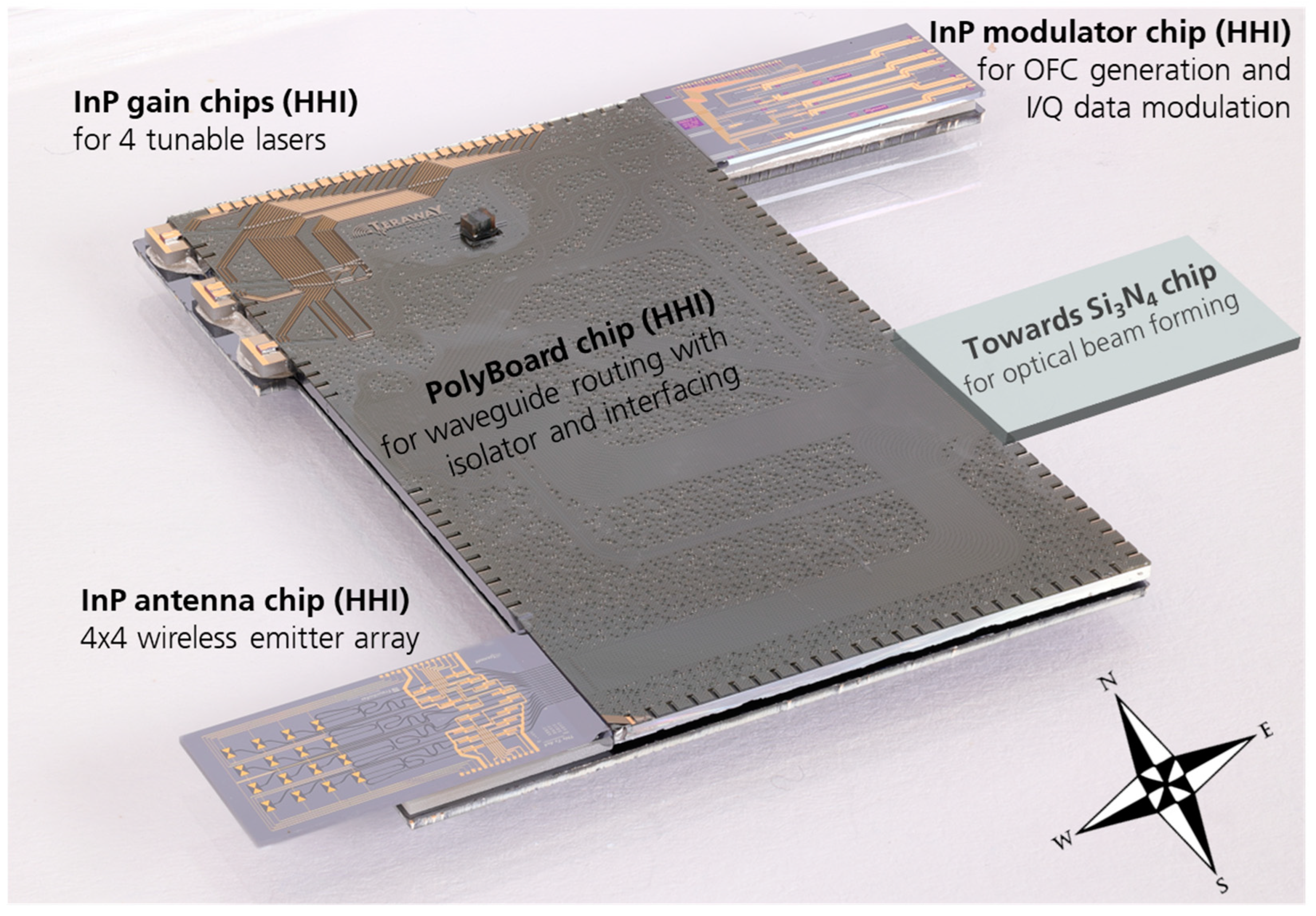
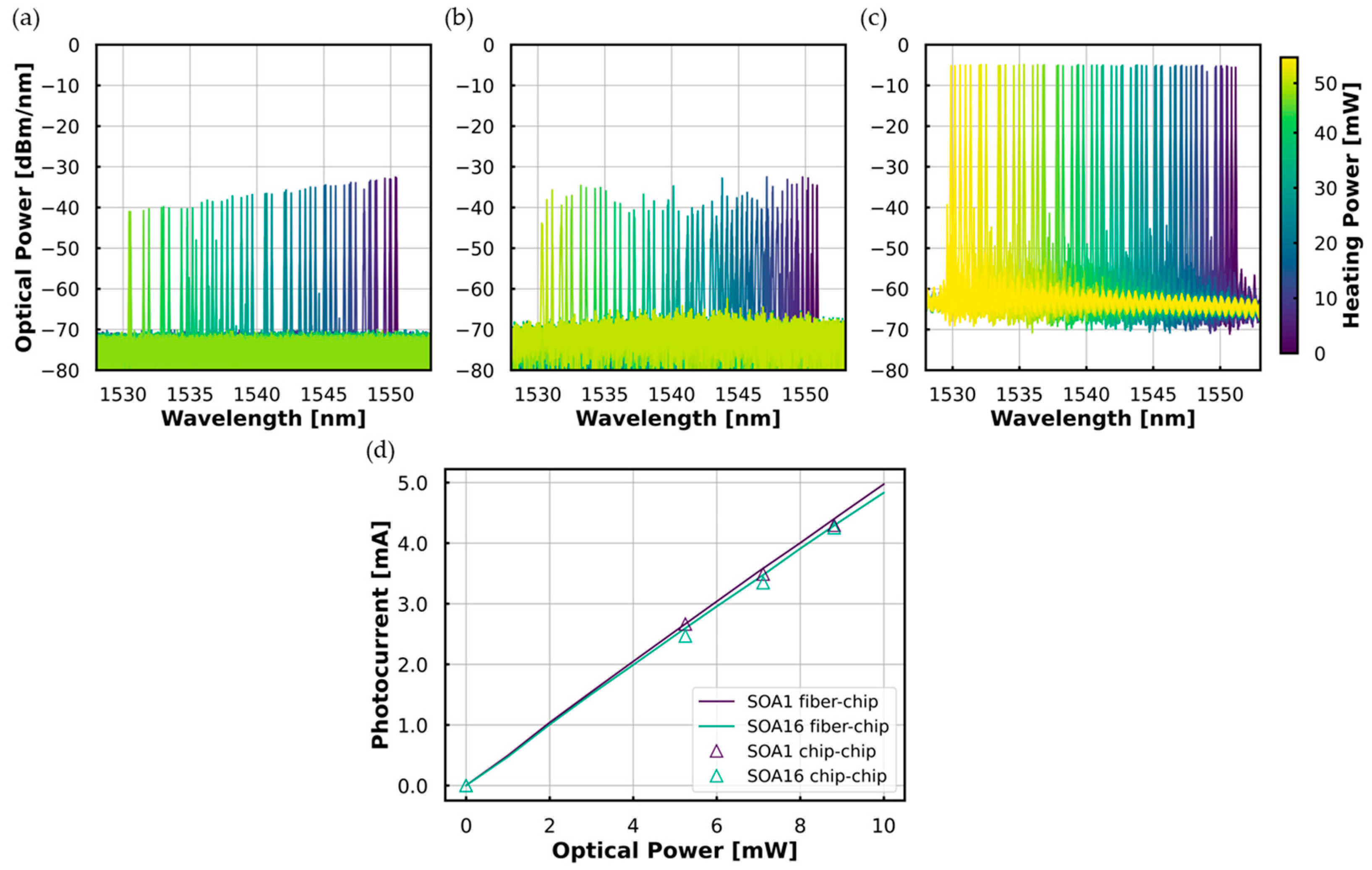
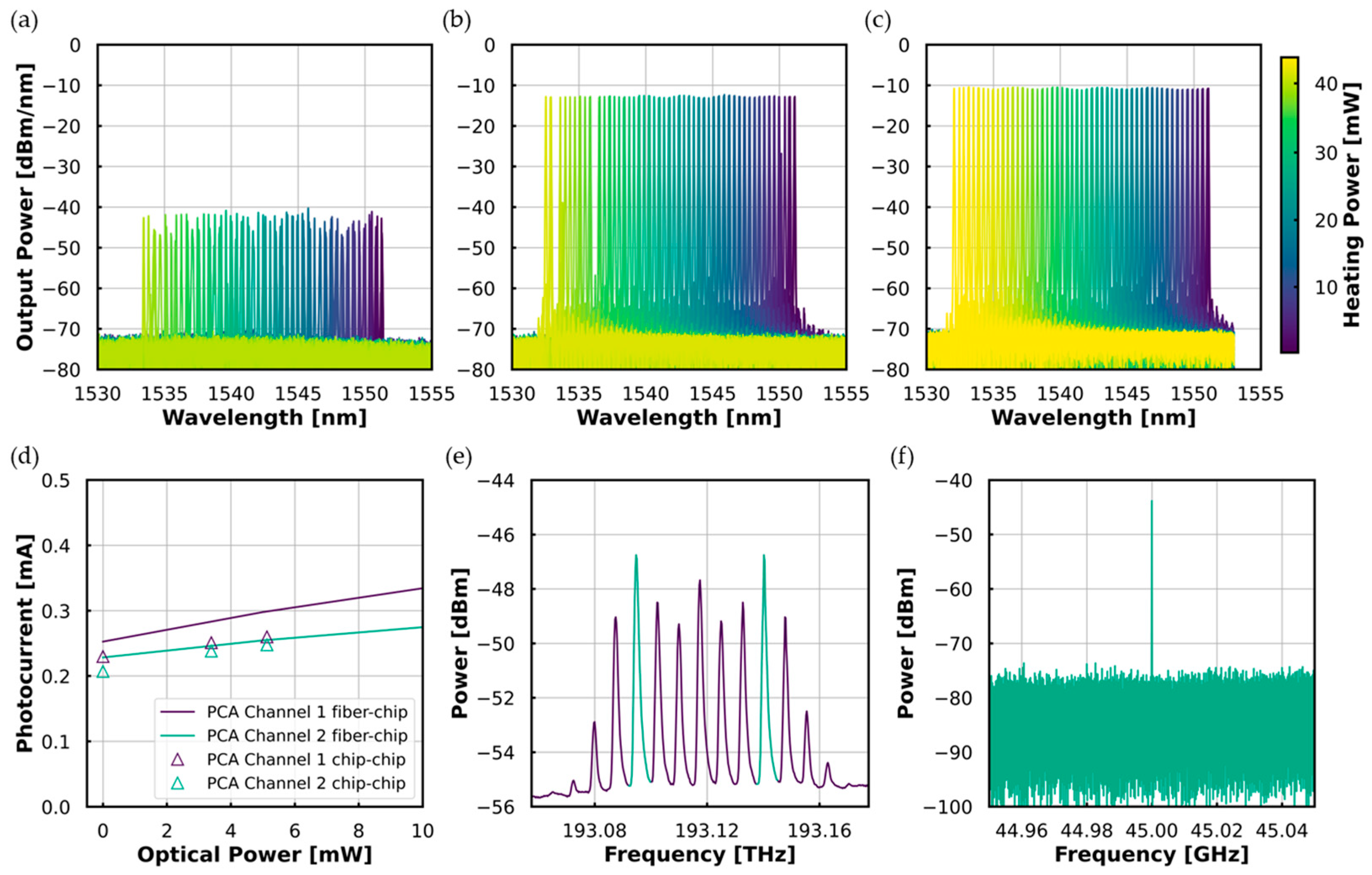
3.2. Hybrid Wireless Transmitter PIC

With the above-mentioned photonic building blocks, the first prototypes of the hybrid wireless transmitter and receiver PIC have been demonstrated. Both PICs use PolyBoard as the motherboard for tunable lasers, waveguide routing with optical isolators, and interfacing with InP and Si3N4 chips. The other active photonic functions, such as the OFC generation, I/Q data modulation, and THz emitter and receivers, as well as the passive functions, such as OBFN based on Si3N4, are integrated on different chiplets. They are butt-coupled on the west and east sides of the PolyBoard based on the current assembly limitations. The active coupling method is used during the coupling process to spare the additional alignment loops for each interface and platform.
Figure 13 shows the assembled wireless transmitter PIC. Starting from the northwest side, four hybrid InP/Polymer tunable DBR lasers are integrated; one is implemented as the master laser, and the rest are implemented as slave lasers for generating phase-locked optical signals. An InP modulator chip is placed on the northeast side with two phase modulators for OFC generation, one I/Q modulator, and one MZM for generating modulated carriers. The phase-locked optical signals are then routed towards the OBFN chip on the southeast side with beam-forming functionality. Finally, the processed optical signals are received by an InP antenna chip with a SOA integrated wireless emitter array in a 4 × 4 configuration.
The assembled PIC is characterized by testing its coupling with various interfaces using a fiber array connected to the PolyBoard chip, with waveguide tap couplers (average insertion loss of 16.6 dB in TE polarization) enabling measurements. A fiber-to-chip coupling loss of 1.0 dB per facet is assumed during the characterization process. Figure 14a,b show the spectra of the hybrid tunable DBR lasers with varying heating power on the grating section, measured after passing through the InP modulator chip. Figure 14c shows the spectra of the slave laser measured directly through the fiber array. Additionally, Figure 14d validates the successful coupling of the InP antenna chip by comparing fiber-chip and chip-chip characterization before and after the assembly. The outermost SOAs are measured.

3.3. Hybrid Wireless Receiver PIC

The receiver PIC follows a configuration similar to that of the transmitter PIC. The InP modulator chip incorporates two cascaded phase modulators to generate the OFC. Instead of using an optical beamforming network, a phased array based on phase shifters and MMIs is integrated on the PolyBoard. This phased array is coupled to the single-channel and two-channel InP antenna chips based on waveguide integrated PCAs, which are located on the southeast side of the PolyBoard chip. The assembled wireless receiver PIC is shown in Figure 15.
The receiver PIC is characterized in a similar manner using a fiber array coupled to the PolyBoard chip. Figure 16a–c show the spectra of the master laser and two slave lasers with varying the heating power on the grating section, while Figure 16d displays the I-V characteristic of the coupled PCA chip. Additionally, the receiver PIC is further characterized to validate the on-chip optical injection locking [84]. As shown in Figure 16e, the OFC is generated by operating the master laser and applying 7.5 GHz RF signals to the cascaded phase modulators. The resulting OFC is measured through the fiber array accessed via the test ports. By locking the slave lasers to the third-order harmonics of the comb, a phase-locked optical beat note at 45 GHz is demonstrated in Figure 16f.

4. Discussion

While the prototype of hybrid wireless transceiver PICs demonstrates significant advancements in realizing complex photonic systems through hybrid integration, several challenges remain, including power budget constraints, thermal management, packaging, and performance optimization of individual building blocks.
Taking the hybrid wireless receiver PIC as an example, the target optical power at the waveguide-integrated PCA exceeds 0 dBm. In an ideal scenario, the hybrid DBR laser is expected to deliver 13 dBm output power. Considering the passive components on the PolyBoard—including the phase shifter network (approximated as three 3-dB couplers, resulting in ~9 dB loss), waveguide propagation losses (~2 dB), and simulated coupling loss (~1.3 dB)—the power budget is already near its limit. This imposes strict requirements on coupling accuracy, the performance of individual chiplets, and overall thermal management, given that all individual components were characterized under controlled lab conditions. Additionally, the limited OFC bandwidth achieved in this work highlights packaging challenges, especially when photonic components require RF connectivity.
Future work should consider power budget optimizations with strategic trade-offs. One potential approach is to distribute complex photonic functionalities across subsystems and incorporate multiple SOAs at different stages to enhance the optical power delivered to antenna arrays, thereby increasing the effective radiated power. Furthermore, the hybrid integration approach can be expanded to include alternative material platforms, such as LiNbO3, to achieve broader OFCs extending into the THz range, enhancing bandwidth and system flexibility. While scaling to larger transmitter and receiver antenna arrays is a natural progression, robust packaging solutions and effective thermal management strategies will be crucial to ensuring reliable operation and efficient heat dissipation.

5. Conclusions

This paper has reviewed the recent development of hybrid PICs for wireless communications at Fraunhofer HHI, focusing on the integration of key photonic subsystems: injection-locked laser sources, photonic THz emitters/receivers, and OPAs. We demonstrated cascaded PMs based on InP, generating OFCs with a 225 GHz bandwidth, and hybrid InP/polymer tunable lasers achieving a locking range of 3.8 GHz in a master–slave configuration. Waveguide-integrated PCAs on the InP platform showed a 22-fold improvement in photoresponse compared to traditional top-illuminated designs, while 1 × 4 arrays of PIN-PDs and PCAs were implemented for scalable wireless communication. The integration of polymer-based OPAs with 1 × 4 InP PIN-PD antenna arrays enabled continuous beam steering across 20° at 300 GHz, with an increased output power of 10.6 dB and improved directivity. Prototypes of hybrid wireless transceiver PICs were successfully assembled and experimentally demonstrated a phase-locked optical beat note at 45 GHz via on-chip OFC generation. These transceivers integrate tunable lasers, on-chip OFC generation, I/Q modulators, and THz emitter/receiver arrays, demonstrating the feasibility of fully integrated PICs for high-speed wireless communication.
In conclusion, the advancements presented in this work demonstrate the potential of hybrid PICs as a key enabler for next-generation wireless networks in the mmWave and THz regimes. By addressing power budget challenges through multi-stage SOA integration, leveraging wider OFCs, and scaling up antenna arrays, hybrid photonic integration technology is poised to play a pivotal role in shaping the future of high-speed wireless communication.

Author Contributions

Conceptualization, T.Q. and D.d.F.; methodology, T.Q.; software, T.Q. and B.S.; validation, T.Q., B.S. and D.d.F.; formal analysis, T.Q. and B.S.; investigation, T.Q. and B.S.; resources, T.Q. and B.S.; data curation, T.Q., B.S., Y.D.G., M.D., S.N., E.A. and N.K.L.; writing—original draft preparation, T.Q.; writing—review and editing, D.d.F., M.S., B.S., Y.D.G., M.D., S.N., M.K. (Martin Kresse), M.W., J.R., K.M., P.W., C.K., L.v.E. and M.K. (Moritz Kleinert); visualization, T.Q. and M.A.; supervision, M.S., N.K., R.B.K. and H.A.; project administration, T.Q., C.Z. and D.d.F.; funding acquisition, D.d.F., C.Z., N.K., R.B.K. and H.A. All authors have read and agreed to the published version of the manuscript.

Funding

This research was funded by the European Commission, through the EU Horizon 2020 project TERAWAY (Grant agreement ID: 871668).

Institutional Review Board Statement

Not applicable.

Informed Consent Statement

Not applicable.

Data Availability Statement

The data related to the paper are available from the corresponding authors upon reasonable request.

Acknowledgments

The authors acknowledge the EU Horizon 2020 project TERAWAY (Grant agreement ID: 871668), the EU Horizon Europe projects SPRINTER (Grant agreement ID: 101070581) and TERA6G (Grant agreement ID: 101096949), all funded by the European Commission, for their support of broader research efforts in this field. The numerical simulations in this work were performed using ANSYS Lumerical software under a commercial license authorized by CADFEM Germany GmbH. We acknowledge ANSYS, Inc. for providing access to their simulation tools under proper licensing agreements. We also sincerely thank Robert Grootjans (r.grootjans@lionix-int.com), Ilka Visscher (i.visscher@lionix-int.com), Ahmad W. Mohammad (a.w.m.mohammad@lionix-int.com), and Chris Roeloffzen (c.g.h.roeloffzen@lionix-int.com) from LioniX International BV for their valuable knowledge contributions on the Si3N4 chip used in this study.

Conflicts of Interest

The authors declare no conflicts of interest.

References

  1. Leitenstorfer, A.; Moskalenko, A.S.; Kampfrath, T.; Kono, J.; Castro-Camus, E.; Peng, K.; Qureshi, N.; Turchinovich, D.; Tanaka, K.; Markelz, A.G.; et al. The 2023 terahertz science and technology roadmap. J. Phys. D Appl. Phys. 2023, 56, 223001. [Google Scholar] [CrossRef]
  2. Song, H.-J.; Lee, N. Terahertz Communications: Challenges in the Next Decade. IEEE Trans. Terahertz Sci. Technol. 2022, 12, 105–117. [Google Scholar] [CrossRef]
  3. Nagatsuma, T.; Ducournau, G.; Renaud, C.C. Advances in terahertz communications accelerated by photonics. Nat. Photonics 2016, 10, 371–379. [Google Scholar] [CrossRef]
  4. Song, H.-J.; Nagatsuma, T. Present and Future of Terahertz Communications. IEEE Trans. Terahertz Sci. Technol. 2011, 1, 256–263. [Google Scholar] [CrossRef]
  5. Nagatsuma, T.; Carpintero, G. Recent Progress and Future Prospect of Photonics-Enabled Terahertz Communications Research. IEICE Trans. Electron. 2015, 98, 1060–1070. [Google Scholar] [CrossRef]
  6. Seeds, A.J.; Shams, H.; Fice, M.J.; Renaud, C.C. TeraHertz Photonics for Wireless Communications. J. Lightwave Technol. 2015, 33, 579–587. [Google Scholar] [CrossRef]
  7. Degli-Eredi, I.; An, P.; Drasbæk, J.; Mohammadhosseini, H.; Nielsen, L.; Tønning, P.; Rommel, S.; Monroy, I.T.; Heck, M.J.R. Millimeter-wave generation using hybrid silicon photonics. J. Opt. 2021, 23, 43001. [Google Scholar] [CrossRef]
  8. Safian, R.; Ghazi, G.; Mohammadian, N. Review of photomixing continuous-wave terahertz systems and current application trends in terahertz domain. Opt. Eng. 2019, 58, 1. [Google Scholar] [CrossRef]
  9. Brown, E.R. THz Generation by Photomixing in Ultrafast Photoconductors. Int. J. High Speed Electron. Syst. 2003, 13, 497–545. [Google Scholar] [CrossRef]
  10. Li, X.; Yu, J.; Zhang, J.; Dong, Z.; Li, F.; Chi, N. A 400G optical wireless integration delivery system. Opt. Express 2013, 21, 18812–18819. [Google Scholar] [CrossRef]
  11. Siew, S.Y.; Li, B.; Gao, F.; Zheng, H.Y.; Zhang, W.; Guo, P.; Xie, S.W.; Song, A.; Dong, B.; Luo, L.W.; et al. Review of Silicon Photonics Technology and Platform Development. J. Lightwave Technol. 2021, 39, 4374–4389. [Google Scholar] [CrossRef]
  12. Rahim, A.; Hermans, A.; Wohlfeil, B.; Petousi, D.; Kuyken, B.; van Thourhout, D.; Baets, R. Taking silicon photonics modulators to a higher performance level: State-of-the-art and a review of new technologies. Adv. Photonics 2021, 3, 24003. [Google Scholar] [CrossRef]
  13. Besancon, C.; Néel, D.; Make, D.; Ramírez, J.M.; Cerulo, G.; Vaissiere, N.; Bitauld, D.; Pommereau, F.; Fournel, F.; Dupré, C.; et al. AlGaInAs Multi-Quantum Well Lasers on Silicon-on-Insulator Photonic Integrated Circuits Based on InP-Seed-Bonding and Epitaxial Regrowth. Appl. Sci. 2022, 12, 263. [Google Scholar] [CrossRef]
  14. Xiang, C.; Jin, W.; Huang, D.; Tran, M.A.; Guo, J.; Wan, Y.; Xie, W.; Kurczveil, G.; Netherton, A.M.; Liang, D.; et al. High-Performance Silicon Photonics Using Heterogeneous Integration. IEEE J. Sel. Top. Quantum Electron. 2022, 28, 8200515. [Google Scholar] [CrossRef]
  15. Gupta, Y.D.; Binet, G.; Diels, W.; Abdeen, O.; Gaertner, T.; Baier, M.; Schell, M. Implementation, Modelling and Verification of High-Speed Mach-Zehnder Phase Modulators in an Open Access InP Foundry Platform. J. Lightwave Technol. 2023, 41, 3498–3504. [Google Scholar] [CrossRef]
  16. Soares, F.; Baier, M.; Gaertner, T.; Grote, N.; Moehrle, M.; Beckerwerth, T.; Runge, P.; Schell, M. InP-Based Foundry PICs for Optical Interconnects. Appl. Sci. 2019, 9, 1588. [Google Scholar] [CrossRef]
  17. Roeloffzen, C.G.H.; Hoekman, M.; Klein, E.J.; Wevers, L.S.; Timens, R.B.; Marchenko, D.; Geskus, D.; Dekker, R.; Alippi, A.; Grootjans, R.; et al. Low-Loss Si3N4 TriPleX Optical Waveguides: Technology and Applications Overview. IEEE J. Sel. Top. Quantum Electron. 2018, 24, 4400321. [Google Scholar] [CrossRef]
  18. Buzaverov, K.A.; Baburin, A.S.; Sergeev, E.V.; Avdeev, S.S.; Lotkov, E.S.; Bukatin, S.V.; Stepanov, I.A.; Kramarenko, A.B.; Amiraslanov, A.S.; Kushnev, D.V.; et al. Silicon Nitride Integrated Photonics from Visible to Mid-Infrared Spectra. Laser Photonics Rev. 2024, 18, 2400508. [Google Scholar] [CrossRef]
  19. Kleinert, M.; Nuck, M.; Conradi, H.; De Felipe, D.; Kresse, M.; Brinker, W.; Zawadzki, C.; Keil, N.; Schell, M. A platform approach towards hybrid photonic integration and assembly for communications, sensing, and quantum technologies based on a polymer waveguide technology. In Proceedings of the 2019 IEEE CPMT Symposium Japan (ICSJ), Kyoto, Japan, 18–20 November 2019; pp. 25–30. [Google Scholar]
  20. Dangel, R.; La Porta, A.; Jubin, D.; Horst, F.; Meier, N.; Seifried, M.; Offrein, B.J. Polymer Waveguides Enabling Scalable Low-Loss Adiabatic Optical Coupling for Silicon Photonics. IEEE J. Sel. Top. Quantum Electron. 2018, 24, 8200211. [Google Scholar] [CrossRef]
  21. Chen, G.; Gao, Y.; Lin, H.-L.; Danner, A.J. Compact and Efficient Thin-Film Lithium Niobate Modulators. Adv. Photonics Res. 2023, 4, 2300229. [Google Scholar] [CrossRef]
  22. Honardoost, A.; Abdelsalam, K.; Fathpour, S. Rejuvenating a Versatile Photonic Material: Thin-Film Lithium Niobate. Laser Photonics Rev. 2020, 14, 2000088. [Google Scholar] [CrossRef]
  23. Zhu, D.; Shao, L.; Yu, M.; Cheng, R.; Desiatov, B.; Xin, C.J.; Hu, Y.; Holzgrafe, J.; Ghosh, S.; Shams-Ansari, A.; et al. Integrated photonics on thin-film lithium niobate. Adv. Opt. Photonics 2021, 13, 242. [Google Scholar] [CrossRef]
  24. Sattari, H.; Prieto, I.; Zarebidaki, H.; Leo, J.; Choong, G.; Arefi, F.; Orvietani, M.; Della Torre, A.; Mettraux, A.; Dubois, F.; et al. Thin-film lithium niobate PICs: Advancements and potential applications in telecom and beyond. In Integrated Photonics Platforms III; SPIE: Strasbourg, France, 2024; pp. 86–89. [Google Scholar]
  25. Burla, M.; Hoessbacher, C.; Heni, W.; Haffner, C.; Fedoryshyn, Y.; Werner, D.; Watanabe, T.; Massler, H.; Elder, D.L.; Dalton, L.R.; et al. 500 GHz plasmonic Mach-Zehnder modulator enabling sub-THz microwave photonics. APL Photonics 2019, 4, 056106. [Google Scholar] [CrossRef]
  26. Andrianopoulos, E.; Tokas, K.; Felipe, D.d.; Theurer, M.; Weigel, M.; Pagano, A.; Kanta, K.; Kresse, M.; Megas, G.; Tsokos, C.; et al. Integrated 800 Gb/s O-band WDM optical transceiver enabled by hybrid InP-polymer photonic integration. J. Opt. Commun. Netw. 2024, 16, D44. [Google Scholar] [CrossRef]
  27. Qian, T.; Deumer, M.; Gupta, Y.D.; Nellen, S.; Schuler, B.; Conradi, H.; Kresse, M.; Reck, J.; Mihov, K.; Kleinert, M.; et al. Hybrid Polymer THz Receiver PIC with Waveguide Integrated Photoconductive Antenna: Concept and 1st Characterization Results. In Proceedings of the Optical Fiber Communication Conference (OFC) 2022, San Diego, CA, USA, 6–10 March 2022; W3D.6. ISBN 978-1-55752-466-9. [Google Scholar]
  28. Conradi, H.; Qian, T.; Kresse, M.; Reck, J.; de Felipe, D.; Kleinert, M.; Weigel, M.; Zawadzki, C.; Keil, N.; Schell, M. Tunable DBR Laser with Integrated Optical Isolator. In Proceedings of the Optical Fiber Communications Conference (OFC) 2021, San Francisco, CA, USA, 6–10 June 2021; pp. 1–3, ISBN 978-1-943580-86-6. [Google Scholar]
  29. Kleinert, M.; de Felipe, D.; Conradi, H.; Kresse, M.; Jehle, L.; Weigel, M.; Qian, T.; Mihov, K.; Reck, J.; Zawadzki, C.; et al. Hybrid Polymer Integration for Communications, Sensing and Quantum Technologies from the Visible to the Infrared. In Proceedings of the 2021 European Conference on Optical Communication (ECOC), Bordeaux, France, 13–16 September 2021; pp. 1–4, ISBN 978-1-6654-3868-1. [Google Scholar]
  30. Yao, J. Microwave Photonic Systems. J. Lightwave Technol. 2022, 40, 6595–6607. [Google Scholar] [CrossRef]
  31. Yao, J. Microwave Photonics. J. Lightwave Technol. 2009, 27, 314–335. [Google Scholar] [CrossRef]
  32. Fan, Y.; Oldenbeuving, R.M.; Roeloffzen, C.G.; Hoekman, M.; Geskus, D.; Heideman, R.G.; Boller, K.-J. 290 Hz Intrinsic Linewidth from an Integrated Optical Chip-based Widely Tunable InP-Si3N4 Hybrid Laser. In Proceedings of the Conference on Lasers and Electro-Optics, Washington, DC, USA, 25–29 June 2017. JTh5C.9. [Google Scholar]
  33. De Felipe, D.; Zhang, Z.; Brinker, W.; Kleinert, M.; Novo, A.M.; Zawadzki, C.; Moehrle, M.; Keil, N. Polymer-Based External Cavity Lasers: Tuning Efficiency, Reliability, and Polarization Diversity. IEEE Photonics Technol. Lett. 2014, 26, 1391–1394. [Google Scholar] [CrossRef]
  34. Xiang, C.; Morton, P.A.; Bowers, J.E. Ultra-narrow linewidth laser based on a semiconductor gain chip and extended Si3N4 Bragg grating. Opt. Lett. 2019, 44, 3825–3828. [Google Scholar] [CrossRef]
  35. Kharas, D.; Plant, J.J.; Loh, W.; Swint, R.B.; Bramhavar, S.; Heidelberger, C.; Yegnanarayanan, S.; Juodawlkis, P.W. High-Power (>300 mW) On-Chip Laser With Passively Aligned Silicon-Nitride Waveguide DBR Cavity. IEEE Photonics J. 2020, 12, 1504612. [Google Scholar] [CrossRef]
  36. Zhang, Y.; Yang, S.; Guan, H.; Lim, A.E.-J.; Lo, G.-Q.; Magill, P.; Baehr-Jones, T.; Hochberg, M. Sagnac loop mirror and micro-ring based laser cavity for silicon-on-insulator. Opt. Express 2014, 22, 17872–17879. [Google Scholar] [CrossRef]
  37. Tang, R.; Kita, T.; Yamada, H. Narrow-spectral-linewidth silicon photonic wavelength-tunable laser with highly asymmetric Mach-Zehnder interferometer. Opt. Lett. 2015, 40, 1504–1507. [Google Scholar] [CrossRef] [PubMed]
  38. Debregeas, H.; Ferrari, C.; Cappuzzo, M.A.; Klemens, F.; Keller, R.; Pardo, F.; Bolle, C.; Xie, C.; Earnshaw, M.P. 2kHz Linewidth C-Band Tunable Laser by Hybrid Integration of Reflective SOA and SiO2 PLC External Cavity. In Proceedings of the 2014 International Semiconductor Laser Conference, Palma de Mallorca, Spain, 7–10 September 2014; pp. 50–51. [Google Scholar]
  39. Maier, P.; Chen, Y.; Xu, Y.; Bao, Y.; Blaicher, M.; Geskus, D.; Dekker, R.; Liu, J.; Dietrich, P.-I.; Peng, H.; et al. Sub-kHz-Linewidth External-Cavity Laser (ECL) With Si3N4 Resonator Used as a Tunable Pump for a Kerr Frequency Comb. J. Lightwave Technol. 2023, 41, 3479–3490. [Google Scholar] [CrossRef]
  40. Xiang, C.; Guo, J.; Jin, W.; Wu, L.; Peters, J.; Xie, W.; Chang, L.; Shen, B.; Wang, H.; Yang, Q.-F.; et al. High-performance lasers for fully integrated silicon nitride photonics. Nat. Commun. 2021, 12, 6650. [Google Scholar] [CrossRef] [PubMed]
  41. De Felipe, D.; Happach, M.; Nellen, S.; Brinker, W.; Kleinert, M.; Zawadzki, C.; Möhrle, M.; Keil, N.; Göbel, T.; Petermann, K.; et al. Hybrid polymer/InP dual DBR laser for 1.5 μm continuous-wave terahertz systems. In Proceedings of the Terahertz, RF, Millimeter, and Submillimeter-Wave Technology and Applications IX SPIE OPTO, San Francisco, CA, USA, 25 February 2016; Sadwick, L.P., Yang, T., Eds.; SPIE: San Francisco, CA, USA, 2016; p. 974719. [Google Scholar]
  42. Wang, M.; Fang, Z.; Zhang, H.; Lin, J.; Zhou, J.; Huang, T.; Zhu, Y.; Li, C.; Yu, S.; Fu, B.; et al. Recent Progresses on Hybrid Lithium Niobate External Cavity Semiconductor Lasers. Materials 2024, 17, 4453. [Google Scholar] [CrossRef]
  43. Zhang, L.; Li, X.; Luo, W.; Shi, J.; Sun, K.; Qiu, M.; Zheng, Z.; Kong, H.; Zhou, J.; Zhang, C.; et al. Review of 1.55 μm Waveband Integrated External Cavity Tunable Diode Lasers. Photonics 2023, 10, 1287. [Google Scholar] [CrossRef]
  44. Qian, T.; Liebermann, P.; Kresse, M.; Mihov, K.; Schell, M. A hybrid photonic integrated signal source with >1.5 THz continuous tunability and <0.25 GHz accuracy for mmW/THz applications. In Proceedings of the 24th European Conference on Integrated Optics, Enschede, The Netherlands, 19–21 April 2023. [Google Scholar]
  45. Pintus, P.; Guo, J.; Jin, W.; Tran, M.A.; Peters, J.; Xiang, C.; Liang, J.; Ohanian, O.J.; Bowers, J.E. 225 GHz Mode-Hop-Free Tuning with a Narrow Linewidth Integrated InP/Si Laser. In CLEO: Science and Innovations; Optica Publishing Group: Washington, DC, USA, 2022; ISBN 978-1-957171-05-0. [Google Scholar]
  46. van Rees, A.; Fan, Y.; Geskus, D.; Klein, E.J.; Oldenbeuving, R.M.; van der Slot, P.J.M.; Boller, K.-J. Ring resonator enhanced mode-hop-free wavelength tuning of an integrated extended-cavity laser. Opt. Express 2020, 28, 5669–5683. [Google Scholar] [CrossRef]
  47. Lang, R. Injection locking properties of a semiconductor laser. IEEE J. Quantum Electron. 1982, 18, 976–983. [Google Scholar] [CrossRef]
  48. Okawachi, Y.; Kim, B.Y.; Lipson, M.; Gaeta, A.L. Chip-scale frequency combs for data communications in computing systems. Optica 2023, 10, 977. [Google Scholar] [CrossRef]
  49. Heffernan, B.M.; Kawamoto, Y.; Maekawa, K.; Greenberg, J.; Amin, R.; Hori, T.; Tanigawa, T.; Nagatsuma, T.; Rolland, A. 60 Gbps real-time wireless communications at 300 GHz carrier using a Kerr microcomb-based source. APL Photonics 2023, 8, 066106. [Google Scholar] [CrossRef]
  50. Chang, L.; Liu, S.; Bowers, J.E. Integrated optical frequency comb technologies. Nat. Photonics 2022, 16, 95–108. [Google Scholar] [CrossRef]
  51. Weng, W.; Kaszubowska-Anandarajah, A.; He, J.; Lakshmijayasimha, P.D.; Lucas, E.; Liu, J.; Anandarajah, P.M.; Kippenberg, T.J. Gain-switched semiconductor laser driven soliton microcombs. Nat. Commun. 2021, 12, 1425. [Google Scholar] [CrossRef]
  52. Sinatkas, G.; Christopoulos, T.; Tsilipakos, O.; Kriezis, E.E. Electro-optic modulation in integrated photonics. J. Appl. Phys. 2021, 130, 010901. [Google Scholar] [CrossRef]
  53. Yu, J.; Li, K.; Chen, Y.; Zhao, L.; Huang, Y.; Li, Y.; Ma, J.; Shan, F. Terahertz-Wave Generation Based on Optical Frequency Comb and Single Mach-Zehnder Modulator. IEEE Photonics J. 2020, 12, 7900808. [Google Scholar] [CrossRef]
  54. Wang, X.; Wang, W.; Zhao, A.; Zhu, D.; Pan, S. Stable OFC generator based on cascaded phase modulators. In Proceedings of the Eleventh International Conference on Information Optics and Photonics (CIOP 2019), Xi’an, China, 6–9 August 2019; Wang, H., Ed.; SPIE: Bellingham, WA, USA, 2019; p. 56, ISBN 9781510631731. [Google Scholar]
  55. Weng, W.; Kaszubowska-Anandarajah, A.; Liu, J.; Anandarajah, P.M.; Kippenberg, T.J. Frequency division using a soliton-injected semiconductor gain-switched frequency comb. Sci. Adv. 2020, 6, eaba2807. [Google Scholar] [CrossRef] [PubMed]
  56. Conradi, H.; Felipe, D.d.; Kleinert, M.; Nuck, M.; Zawadzki, C.; Scheu, A.; Keil, N.; Schell, M. High Isolation Optical Isolator: A new Building Block for PolyBoard Photonic Integrated Circuits. In Proceedings of the 2018 European Conference on Optical Communication (ECOC), Rome, Italy, 23–27 September 2018; pp. 1–3, ISBN 978-1-5386-4862-9. [Google Scholar]
  57. Nagatsuma, T.; Ito, H.; Ishibashi, T. High-power RF photodiodes and their applications. Laser Photonics Rev. 2009, 3, 123–137. [Google Scholar] [CrossRef]
  58. Nellen, S.; Ishibashi, T.; Deninger, A.; Kohlhaas, R.B.; Liebermeister, L.; Schell, M.; Globisch, B. Experimental Comparison of UTC- and PIN-Photodiodes for Continuous-Wave Terahertz Generation. J. Infrared Millimeter Terahertz Waves 2020, 41, 343–354. [Google Scholar] [CrossRef]
  59. Deumer, M.; Nellen, S.; Lauck, S.; Keyvaninia, S.; Berrios, S.; Kieper, M.; Schell, M.; Kohlhaas, R.B. Ultra-Wideband PIN-PD THz Emitter with > 5.5 THz Bandwidth. J. Infrared Millimeter Terahertz Waves 2024, 45, 831–840. [Google Scholar] [CrossRef]
  60. Seddon, J.P.; Natrella, M.; Lin, X.; Graham, C.; Renaud, C.C.; Seeds, A.J. Photodiodes for Terahertz Applications. IEEE J. Sel. Top. Quantum Electron. 2022, 28, 3801612. [Google Scholar] [CrossRef]
  61. Deumer, M.; Breuer, S.; Berrios, S.; Keyvaninia, S.; Schwanke, G.; Schwenson, L.; Lauck, S.; Liebermeister, L.; Nellen, S.; Schell, M.; et al. Continuous wave THz receivers with rhodium-doped InGaAs enabling 132 dB dynamic range. Opt. Express 2024, 32, 29855–29867. [Google Scholar] [CrossRef]
  62. Deumer, M.; Breuer, S.; Kohlhaas, R.; Nellen, S.; Liebermeister, L.; Lauck, S.; Schell, M.; Globisch, B. Continuous wave terahertz receivers with 4.5 THz bandwidth and 112 dB dynamic range. Opt. Express 2021, 29, 41819. [Google Scholar] [CrossRef]
  63. Fernandez Olvera, A.; Roggenbuck, A.; Dutzi, K.; Vieweg, N.; Lu, H.; Gossard, A.; Preu, S. International System of Units (SI) Traceable Noise-Equivalent Power and Responsivity Characterization of Continuous Wave ErAs:InGaAs Photoconductive Terahertz Detectors. Photonics 2019, 6, 15. [Google Scholar] [CrossRef]
  64. Nellen, S.; Lauck, S.; Peytavit, E.; Szriftgiser, P.; Schell, M.; Ducournau, G.; Globisch, B. Coherent Wireless Link at 300 GHz With 160 Gbit/s Enabled by a Photonic Transmitter. J. Lightwave Technol. 2022, 40, 4178–4185. [Google Scholar] [CrossRef]
  65. Nellen, S.; Lauck, S.; Schwanke, G.; Deumer, M.; Kohlhaas, R.B.; Liebermeister, L.; Schell, M.; Globisch, B. Radiation pattern of planar optoelectronic antennas for broadband continuous-wave terahertz emission. Opt. Express 2021, 29, 8244–8257. [Google Scholar] [CrossRef] [PubMed]
  66. Deumer, M.; Nellen, S.; Berrios, S.; Breuer, S.; Keyvaninia, S.; Liebermeister, L.; Schell, M.; Kohlhaas, R.B. Advancing terahertz photomixers through the integration of photoconductive antennas with optical waveguides. APL Photonics 2025, 10, 036105. [Google Scholar] [CrossRef]
  67. Deumer, M.; Nellen, S.; Breuer, S.; Kohlhaas, R.B.; Schwenson, L.; Wenzel, K.; Liebermeister, L.; Schell, M.; Globisch, B. Waveguide-integrated photoconductive THz receivers. In Proceedings of the 2022 47th International Conference on Infrared, Millimeter and Terahertz Waves (IRMMW-THz), Delft, The Netherlands, 28 August–2 September 2022; pp. 1–2. [Google Scholar]
  68. Nellen, S.; Qian, T.; Schwanke, G.; Lauck, S.; Felipe, D.d.; Kleinert, M.; Deumer, M.; Liebermeister, L.; Baier, M.; Globisch, B.; et al. Photonic-enabled beam steering at 300 GHz using a photodiode-based antenna array and a polymer-based optical phased array. Opt. Express 2022, 30, 44701–44716. [Google Scholar] [CrossRef]
  69. Heck, M.J. Highly integrated optical phased arrays: Photonic integrated circuits for optical beam shaping and beam steering. Nanophotonics 2017, 6, 93–107. [Google Scholar] [CrossRef]
  70. Che, M.; Matsuo, Y.; Kanaya, H.; Ito, H.; Ishibashi, T.; Kato, K. Optoelectronic THz-Wave Beam Steering by Arrayed Photomixers With Integrated Antennas. IEEE Photonics Technol. Lett. 2020, 32, 979–982. [Google Scholar] [CrossRef]
  71. Uchendu, I.; Kelly, J.R. Survey of Beam Steering Techniques Available for Millimeter Wave Applications. PIER B 2016, 68, 35–54. [Google Scholar] [CrossRef]
  72. Guo, Y.; Guo, Y.; Li, C.; Zhang, H.; Zhou, X.; Zhang, L. Integrated Optical Phased Arrays for Beam Forming and Steering. Appl. Sci. 2021, 11, 4017. [Google Scholar] [CrossRef]
  73. Zhang, H.; Zhang, Z.; Lv, J.; Peng, C.; Hu, W. Fast beam steering enabled by a chip-scale optical phased array with 8 × 8 elements. Opt. Commun. 2020, 461, 125267. [Google Scholar] [CrossRef]
  74. Lu, P.; Haddad, T.; Tebart, J.; Roeloffzen, C.; Stöhr, A. Photonic Integrated Circuit for Optical Phase Control of 1 × 4 Terahertz Phased Arrays. Photonics 2022, 9, 902. [Google Scholar] [CrossRef]
  75. Carpintero, G.; Headland, D.; Schwanke, G.; Deumer, M.; Nellen, S.; Lauck, S.; Liebermeister, L.; Spanidou, K.; Ali, M.; Rivera, A.; et al. Photonic-Enabled Terahertz Phase Arrays Using Dielectric Rod Waveguides for 6G Wireless Communications. In Proceedings of the 2024 IEEE/MTT-S International Microwave Symposium—IMS 2024, Washington, DC, USA, 16–21 June 2024; pp. 74–77. [Google Scholar]
  76. Fu, X.; Yang, F.; Liu, C.; Wu, X.; Cui, T.J. Terahertz Beam Steering Technologies: From Phased Arrays to Field-Programmable Metasurfaces. Adv. Opt. Mater. 2020, 8, 1900628. [Google Scholar] [CrossRef]
  77. Shao, Z.; Shen, R.; Xia, W.; Ghasempour, Y.; Sengupta, K.; Rangan, S. A Hybrid Antenna-Metasurface Architecture for mmWave and THz Massive MIMO. In Proceedings of the 2023 57th Asilomar Conference on Signals, Systems, and Computers, Pacific Grove, CA, USA, 29 October–1 November 2023; pp. 1610–1616, ISBN 979-8-3503-2574-4. [Google Scholar]
  78. Afeef, L.; Arslan, H. Beam Squint Effect in Multi-Beam mmWave Massive MIMO Systems. In Proceedings of the 2022 IEEE 96th Vehicular Technology Conference (VTC2022-Fall), London, UK, 26–29 September 2022; pp. 1–5, ISBN 978-1-6654-5468-1. [Google Scholar]
  79. Wang, B.; Gao, F.; Xing, C.; An, J.; Li, G.Y. Wideband Beamforming for Hybrid Phased Array Terahertz Systems. In Proceedings of the ICC 2021—IEEE International Conference on Communications, Montreal, QC, Canada, 14–23 June 2021; pp. 1–6, ISBN 978-1-7281-7122-7. [Google Scholar]
  80. Wang, B.; Jian, M.; Gao, F.; Li, G.Y.; Lin, H. Beam Squint and Channel Estimation for Wideband mmWave Massive MIMO-OFDM Systems. IEEE Trans. Signal Process. 2019, 67, 5893–5908. [Google Scholar] [CrossRef]
  81. Camponeschi, F.; Gemmato, V.; Scotti, F.; Rinaldi, L.; Mohammad, A.W.; Roeloffzen, C.G.; van Dijk, P.W.; Ghelfi, P. Multibeam Beamforming Demonstration of a Hybrid Integrated Photonic Module for a Synthetic Aperture Radar Receiver. J. Lightwave Technol. 2024, 42, 7604–7611. [Google Scholar] [CrossRef]
  82. Reza, M.; Mohammad, A.; Serafino, G.; Roeloffzen, C.; van Dijk, P.; Mohammadhosseini, H.; Abbasi, A.; Desoete, B.; Ghelfi, P. Design of an Integrated-Photonics RF Beamformer for Multi-Beam Satellite Synthetic Aperture Radar. In Proceedings of the 2020 International Topical Meeting on Microwave Photonics (MWP), Matsue, Japan, 24–26 November 2020; pp. 87–90. [Google Scholar]
  83. Tsokos, C.; Andrianopoulos, E.; Raptakis, A.; Lyras, N.; Gounaridis, L.; Groumas, P.; Timens, R.B.; Visscher, I.; Grootjans, R.; Wefers, L.S.; et al. True Time Delay Optical Beamforming Network Based on Hybrid Inp-Silicon Nitride Integration. J. Lightwave Technol. 2021, 39, 5845–5854. [Google Scholar] [CrossRef]
  84. Andrianopoulos, E.; Lyras, N.K.; Qian, T.; Deumer, M.; Megas, G.; Schwanke, G.; Gupta, Y.D.; Groumas, P.; Tegegne, Z.G.; Schuler, B.; et al. Demonstration of On-Chip Optical Frequency Comb Generation and Optical Injection Locking. In Proceedings of the Optical Fiber Communication Conference (OFC) 2024, San Diego, CA, USA, 24–28 March 2024. [Google Scholar]
Figure 1. An optical injection locking system for generating phase-locked optical signals.
Photonics 12 00371 g001
Figure 2. Hybrid InP/polymer tunable DBR laser: (a) cross-sectional schematic; (b) example micrograph of a dual hybrid InP/polymer tunable DBR laser, combined with a Y-junction coupler to the output; (c) spectral analysis for determining the injection locking range as a function of internal injection ratio R i n t and detuning frequency Δf.
Photonics 12 00371 g002
Figure 3. (a) InP chip with two cascaded PMs for generating OFCs; SOA is integrated after the second PM, and the coupling interfaces are facilitated by spot-size converters (SSCs); (b) example of generated OFC spectrum. The measured OFC would support a bandwidth of 225 GHz.
Photonics 12 00371 g003
Figure 4. Characterization of an InP MZM: (a) DC ER map of a 5 mm long MZM [15]; (b) high-frequency response of InP MZM with different lengths [15]; (c) eye diagrams of a 5 mm long MZM for NRZ 64 Gbps, NRZ 80 Gbps, PAM4 24 GBd. [15].
Photonics 12 00371 g004
Figure 5. On-chip integrated optical isolator. (a) Close-up image of the on-chip integrated optical isolator. (b) Performance characterization of the optical isolator, demonstrating an on-chip loss of less than 0.8 dB at 1550 nm and an isolation exceeding 32 dB for backward-propagating TE-polarized light [29].
Photonics 12 00371 g005
Figure 6. Photomixing using a waveguide-integrated PIN-PD and device micrographs. (a) Schematic of the photomixing scheme for an I/Q-modulated optical beat signal using a PIN-PD. (b) Micrograph and scanning electron micrograph of a waveguide-integrated PIN-PD chip with bow-tie antenna for THz radiation.
Photonics 12 00371 g006
Figure 7. Photomixing using a waveguide-integrated PCA and device micrographs. (a) Schematic of the photomixing process for an optical beat signal using a PCA. (b) Micrograph and scanning electron micrograph of the novel waveguide-integrated PCA chip [67].
Photonics 12 00371 g007
Figure 8. Fabricated 1 × 4 THz emitter array and its packaging. (a) Micrograph of the fabricated 1 × 4 THz emitter array based on PIN-PDs and integrated with SOAs [68]. (b) The CAD model of the packaged antenna array [68]. (c) The packaged module [68].
Photonics 12 00371 g008
Figure 9. Micrograph of fabricated 1 × 4 THz receiver array based on waveguide integrated PCA.
Photonics 12 00371 g009
Figure 10. Illustration of the schematic design of OPA targeted for THz beam steering.
Photonics 12 00371 g010
Figure 11. (a) Photograph of the assembled and packaged OPA chip. Wire bonding to a multi-pin plug allows stable connection and driving of the OPA in the beam steering testbed. The augmented layout (b) shows the polymer-based OPA chip with four thermo-optical phase shifters (TOPS) to set the phase of the beat signal at the respective output port [68].
Photonics 12 00371 g011
Figure 12. Cross-section of (a) InP SSC; (b) PolyBoard taper, with typical layer thicknesses for the polymer top cladding (ttop) and polymer bottom cladding (tbottom) of 40 µm and 80 µm, respectively; (c) Si3N4 ADS waveguide for HIC (left) and LIC (right), with bottom stripe thickness tg1 = 75 nm, intermediate layer thickness tint = 100 nm, top stripe thickness tg2 = 175 nm, and an etching angle of αg = 82°. The typical layer thicknesses for the SiO2 bottom cladding (tb) and the top cladding (tc) are 8 µm and 15 μm [17]. Simulation of power transmission between different waveguide interfaces: (d) InP and PolyBoard; (e) Si3N4 HIC and PolyBoard; (f) Si3N4 LIC and PolyBoard.
Photonics 12 00371 g012
Figure 13. Hybrid wireless transmitter PIC integrating InP, PolyBoard, and Si3N4 platforms.
Photonics 12 00371 g013
Figure 14. Characterization of the assembled THz transmitter PIC. By varying the power applied onto the grating heater, tuning spectra have been recorded: (a) the master laser going through the InP modulator PIC; (b) the slave laser going through the InP modulator PIC; (c) the slave laser measured directly using a fiber array. (d) Comparison of fiber-to-chip and chip-to-chip characterization based on the photocurrent generated in the outermost SOAs at varying optical power levels.
Photonics 12 00371 g014
Figure 15. Hybrid wireless receiver PIC integrating InP and PolyBoard platforms.
Photonics 12 00371 g015
Figure 16. Characterization of the assembled THz receiver PIC. By varying the power applied onto the grating heater, tuning spectra have been recorded: (a) The master laser going through the InP modulator chip; (b) the slave laser 1; (c) the slave laser 2. (d) Comparison between fiber-chip and chip-chip characterization of the two-channel PCA at different optical power levels. (e) On-chip OFC with a spacing of 7.5 GHz is generated through the cascaded phase modulators and measured through the test ports. The comb lines marked in green are used for injection locking [84]. (f) Phase-locked optical beat note measured at 45 GHz [84].
Photonics 12 00371 g016
Table 1. Qualitative comparison of functionalities offered on different photonic platforms. N/A = not available; + = possible; ++ = good; +++ = very good.
PlatformsWaveguide
Loss
Routing CapabilityHigh-Speed
Modulation
Tunable
Lasers
Optical
Isolator
O/E
Functionalities (e.g., THz Antenna)
InP+++++++N/A+++
PolyBoard+++++N/A++++N/A
Si3N4++++++N/A+++N/AN/A
Table 2. Waveguide properties of each material platform. N/A = not applicable.
Platformsneff @1550 nmMFDx,y [µm]Waveguide Width [µm]Simulated Coupling Loss Towards
PolyBoard [dB]
InP [16]3.2(3.5, 4.4)–(10.0, 7.0)[0.1–1.0]1.3
PolyBoard1.46–1.45(4.3, 4.3)–(9.0, 7.8)[0.8–3.2]N/A
Si3N4 [17]1.535–1.446(1.5, 1.2)–(10.0, 10.0)[0.8–3.7]0.1
Disclaimer/Publisher’s Note: The statements, opinions and data contained in all publications are solely those of the individual author(s) and contributor(s) and not of MDPI and/or the editor(s). MDPI and/or the editor(s) disclaim responsibility for any injury to people or property resulting from any ideas, methods, instructions or products referred to in the content.

