Review

Metasurfaces in Optical Biosensing: Revolutionizing Detection Techniques and Shaping the Future

1
Department of Electrical, Electronics and Communication Engineering, Galgotias University, Greater Noida 201308, Uttar Pradesh, India
2
Galgotias Multi-Disciplinary Research & Development Cell (G-MRDC), Galgotias University, Greater Noida 201308, Uttar Pradesh, India
3
Department of Electronics and Communication Engineering, UCRD, Chandigarh University, Mohali 140413, Punjab, India
4
Amity School of Engineering and Technology, Amity University Haryana, Amity Education Valley, Gurugram, Manesar 122413, Haryana, India
*
Author to whom correspondence should be addressed.
Photonics 2025, 12(4), 360; https://doi.org/10.3390/photonics12040360
Submission received: 27 February 2025 / Revised: 7 April 2025 / Accepted: 8 April 2025 / Published: 10 April 2025
(This article belongs to the Special Issue Optical Metasurfaces: Applications and Trends)

Abstract

:
Metasurfaces have been widely investigated across the disciplines of optical biosensing due to their exceptional ability to manipulate electromagnetic fields. Consequently, over the past few years, there has been growing interest in the application of metasurfaces in optical biosensors in the field of biomedical sensing. While being label-free and offering real-time tracking, high sensitivity, and a quick response are among the benefits of conventional optical biosensors, the incorporation of metasurfaces improves their wavefront manipulation, selectivity for versatile sensing, and capacity for device miniaturization to satisfy increasingly complex application requirements. Furthermore, there is a lack of comprehensive evaluations that address the current research developments and future possibilities, despite the encouraging advancements in this emerging field. Hence, this work provides a comprehensive review and serves as a valuable resource for researchers exploring metasurface-based optical biosensors. This review delves into defining the basic sensing concepts, design procedures, and important figures of merit (FOM) for metasurface-based optical biosensors and their applications, including the detection of numerous analytes, such as viruses, toxins, antibodies, tumors, and drugs and the monitoring of blood sugar. Furthermore, presenting a critical evaluation of structural fabrication techniques with a view toward potential future commercialization, this review ends by highlighting several fascinating areas for further investigation. For this review article, a total of 5844 effective documents about metasurface optical biosensors were retrieved from the Scopus database. The VOSviewer version 1.6.20 bibliometric software was used for the scientific analysis of the data retrieved from the Scopus database from 2010 to 2025.

1. Introduction

Bulk materials with a variety of crystal forms are created when atoms and molecules arrange themselves in three or two dimensions into an organized and periodic formation. The artificial manufacturing of micro-/nanostructures, or “meta-atoms”, that replicate the configurations of atoms and molecules present in natural materials is the fundamental concept behind metamaterials and metasurfaces [1,2]. Bulk materials with this artificial architecture acquire unique electromagnetic properties, including a zero or negative refractive index, zero or negative magnetic permeability, and a zero or negative dielectric constant, among others. In particular, metasurfaces, also identified as two-dimensional variants of metamaterials, are focused on the two-dimensional configurations of these synthetic micro-/nanostructures. Metasurfaces are frequently composed of dielectrics (like silicon) along with metals (like gold and silver). These nanostructures’ shapes, dimensions, spacing, and geometries are all intended to regulate the polarization, amplitude, or phase of impinging light waves. As a result, specific optical reactions like resonance modes such as guided-mode resonances or simply localized surface plasmon resonances (LSPR) are produced [3]. Metasurfaces have attracted a great deal of interest in a variety of applications, such as wireless data transmission [4], solar energy harvesting [5], cloaking [6], polarizers [7], radar [8], quantum computing [9], biomedical imaging [10], and sensing [11], etc., precisely due to their remarkable ability to manipulate optical/electromagnetic fields. Moreover, they exhibit lower energy losses, minimized space requirements, and reduced processing difficulty and costs when compared to metamaterials [12].
Devices known as optical biosensors detect biological molecules by transforming biological interactions like the binding of an antigen with an antibody into measurable light signals [13,14]. Metasurfaces can be used to create optical biosensors with increased sensitivity, a reduced size, and more flexible detection capabilities, which makes them useful instruments for biomedical research, the tracking of the environment, and medical diagnostics [15,16,17]. Metasurface-based optical biosensors have gained more attention in biological sensing investigations over the past several years because of their capacity to quickly analyze data and label samples. Based on the concepts of absorption, emission, scattering, and changes in refractive index, they leverage the chemical interactions that occur due to an impinging light wave on the sensor surface to identify tiny molecules [18,19]. Thus, it becomes imperative to investigate various forms of optical biosensors, such as surface plasmon resonance (SPR) biosensors [20], LSPR [21], photonic waveguides [22], optical resonators [23], and optical fibers [24]. The SPR detector, for instance, has been rather well studied and used in applications because of its excellent sensitivity, fast response time, and real-time detection capabilities. However, at the same time, certain conventional SPR biosensors exhibit poor selectivity in complex biological fluids and have large structures [25]. Metasurface biosensors are one of the most important breakthroughs for the next generation of biosensing chips because of their great optical manipulation capabilities, integration or miniaturization, and multiplexed or multifunctional detection. Furthermore, optical biosensors based on metasurfaces are still in the emerging stages; hence, a thorough assessment of the recent progress in this field, along with the future pathways of research, has not been included in the mainstream discussion over the past few years concerning this field. Therefore, an attempt to bridge this gap is provided in this bibliometric review. A detailed bibliometric analysis is presented in Section 2. This section also delves into the fundamental principles of optical biosensing using metasurfaces. After this, Section 3 provides an in-depth discussion of various fabrication techniques for metasurface-based optical biosensors, followed by a comparative and parametric analysis of various designs in terms of several significant applications in Section 4. It carefully describes particular uses for biomedical sensing, including in situ drug tracking, virus detection, blood glucose estimation, and early cancer detection. The conclusions and future scope of this review are presented in Section 5.

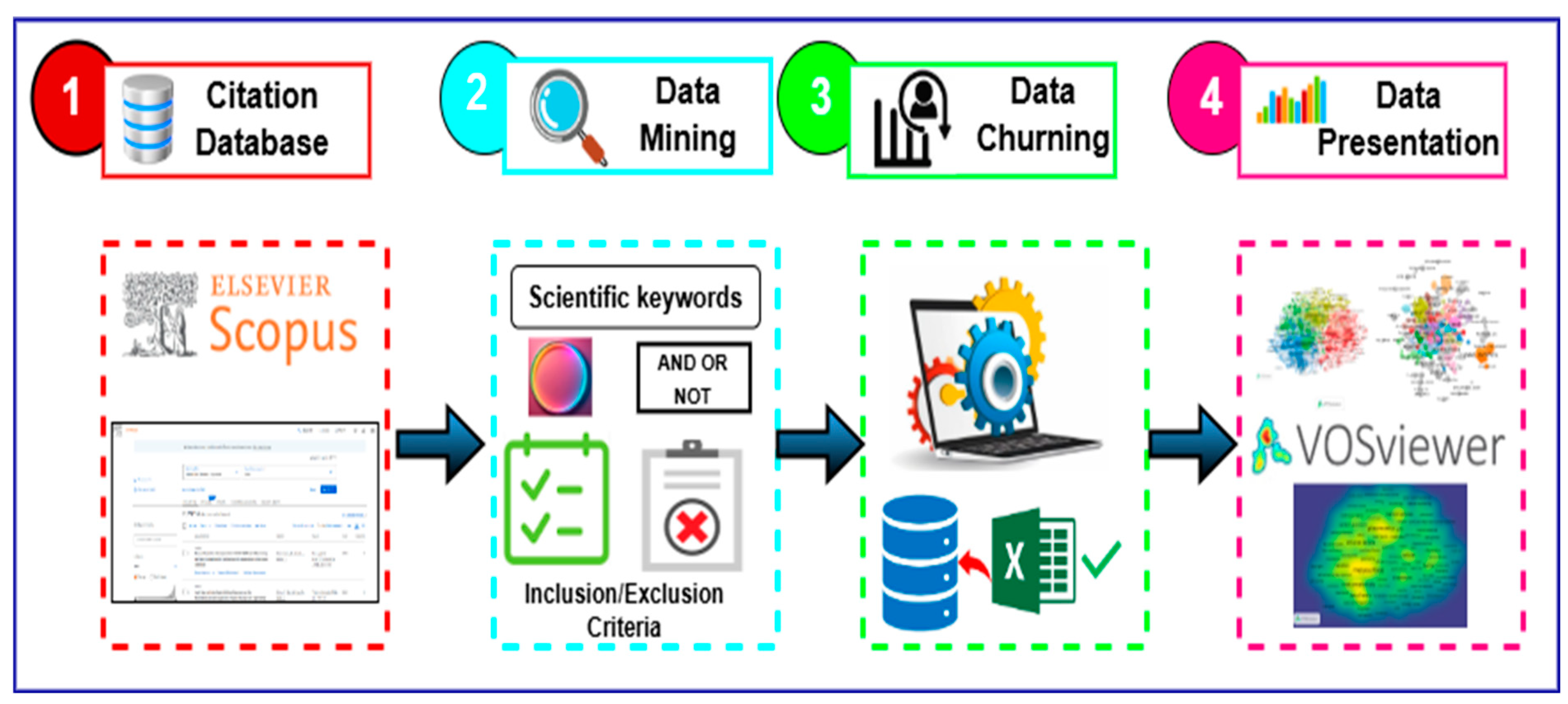
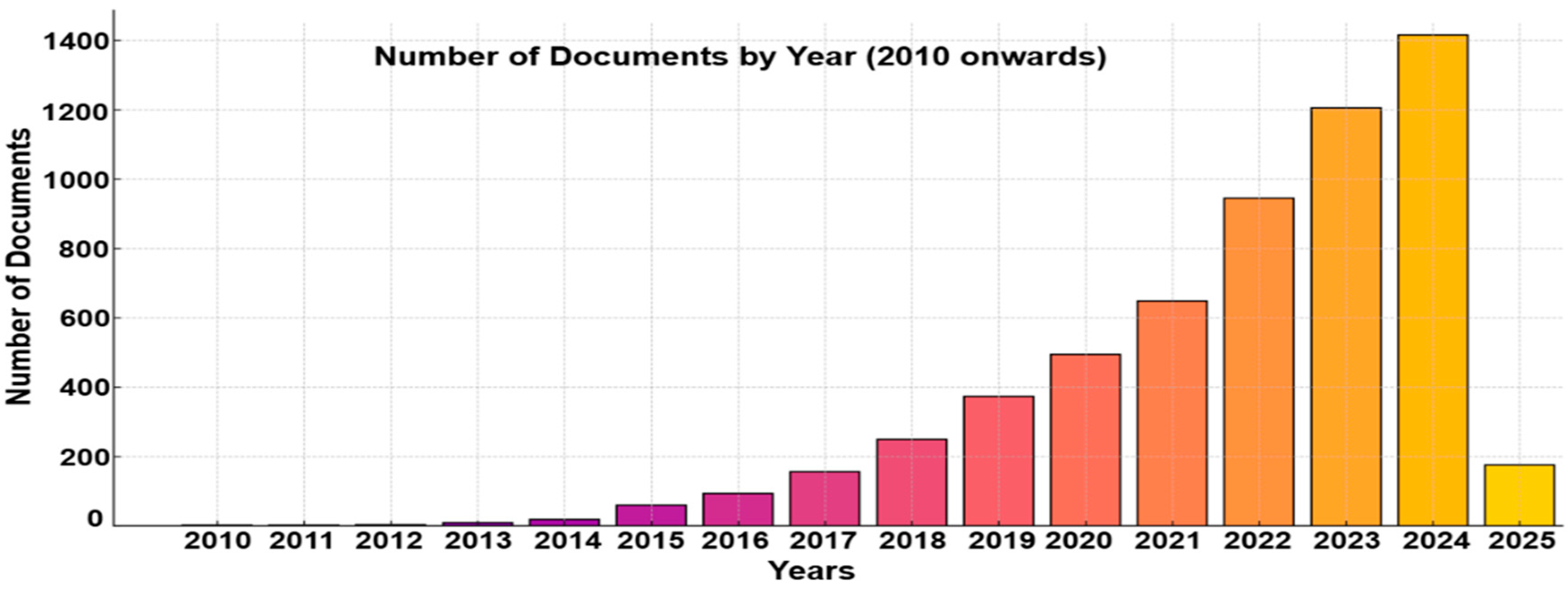
2. Data Collection and Method

The literature documents selected for this review article were retrieved from the Scopus database using an advanced query method to ensure the accuracy and precision of the original data. The keywords used for the retrieval were “metasurfaces AND optical AND biosensor”, and several search criteria were implemented: (1) timespan—2010–2025, (2) language—English; (3) document type—article, review; (4) source type—journal. Furthermore, based on these criteria, 5844 effective documents were retrieved from the Scopus database. Because of its broad academic coverage, superior peer-reviewed sources, and sophisticated indexing features, the Scopus database was selected as a dependable and exhaustive resource for bibliometric analysis. The accuracy and applicability of the data gathered for this study were enhanced by Scopus’s well-structured metadata and wide interdisciplinary coverage when compared to other databases.
The strong network visualization and bibliometric mapping features of the VOSviewer software were the main reasons that we chose it to examine the connections between important keywords, authors, and research trends in this domain. The detailed steps that were involved in the methodology are depicted in Figure 1.

2.1. Statistical Analysis of Metasurface Optical Biosensors

The total number of research articles based on metasurface optical biosensors that were published each year is depicted in Figure 2. The research trends show only two articles published in 2010, and there were rapid and positive changes in the publications until 2025 in the field of metasurface-based optical biosensors. Metasurface-based optical biosensor research has drawn participants from a wide range of backgrounds. An increasing number of nations have started to focus on research and applications in this domain.

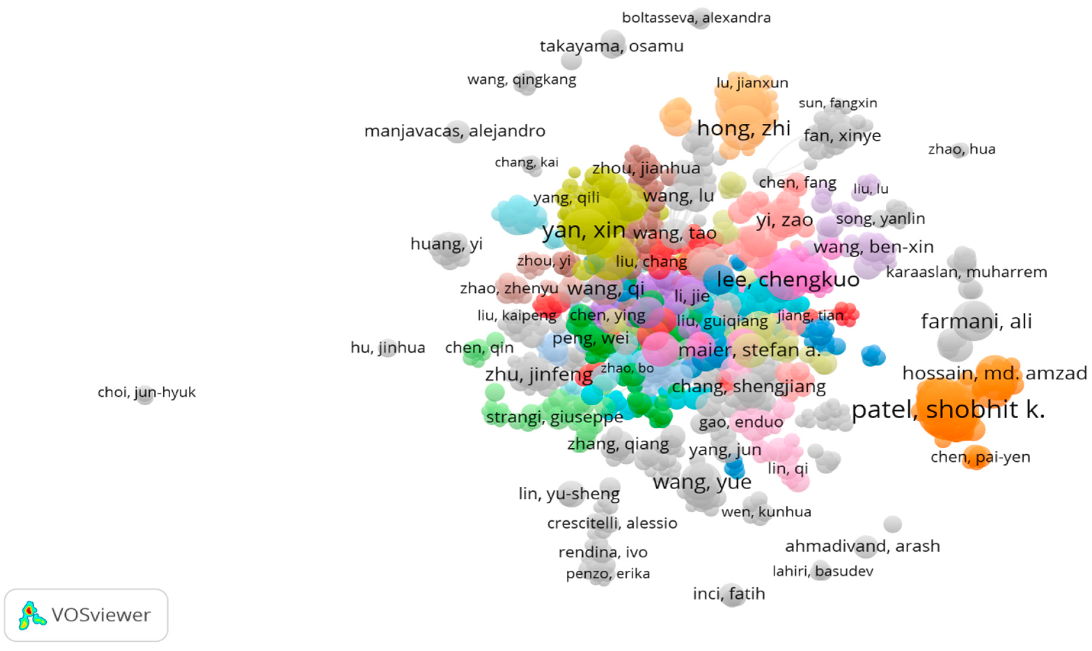
2.1.1. Co-Authorship Analysis of Authors

The collaborative network map of authors based on the search criteria to determine the contributions of different scholars is depicted in Figure 3. The isolated subnetworks depict the lack of interconnection among these authors. The analysis shows that there are 1000 items divided into 48 clusters, having around 5550 links. It can be summarized that the total link strength is 15,114 for the retrieved data from Scopus. It can be concluded that a few authors have conducted research independently, with less connection among the researchers. The top 10 most productive authors in terms of the total documents, citation counts, and total link strength are presented in Table 1. It can be summarized that the author Patel has published 74 documents, followed by Yan with 49 documents. It can also be concluded that the author Lee has the highest number of citations at 1056, with 41 publications.

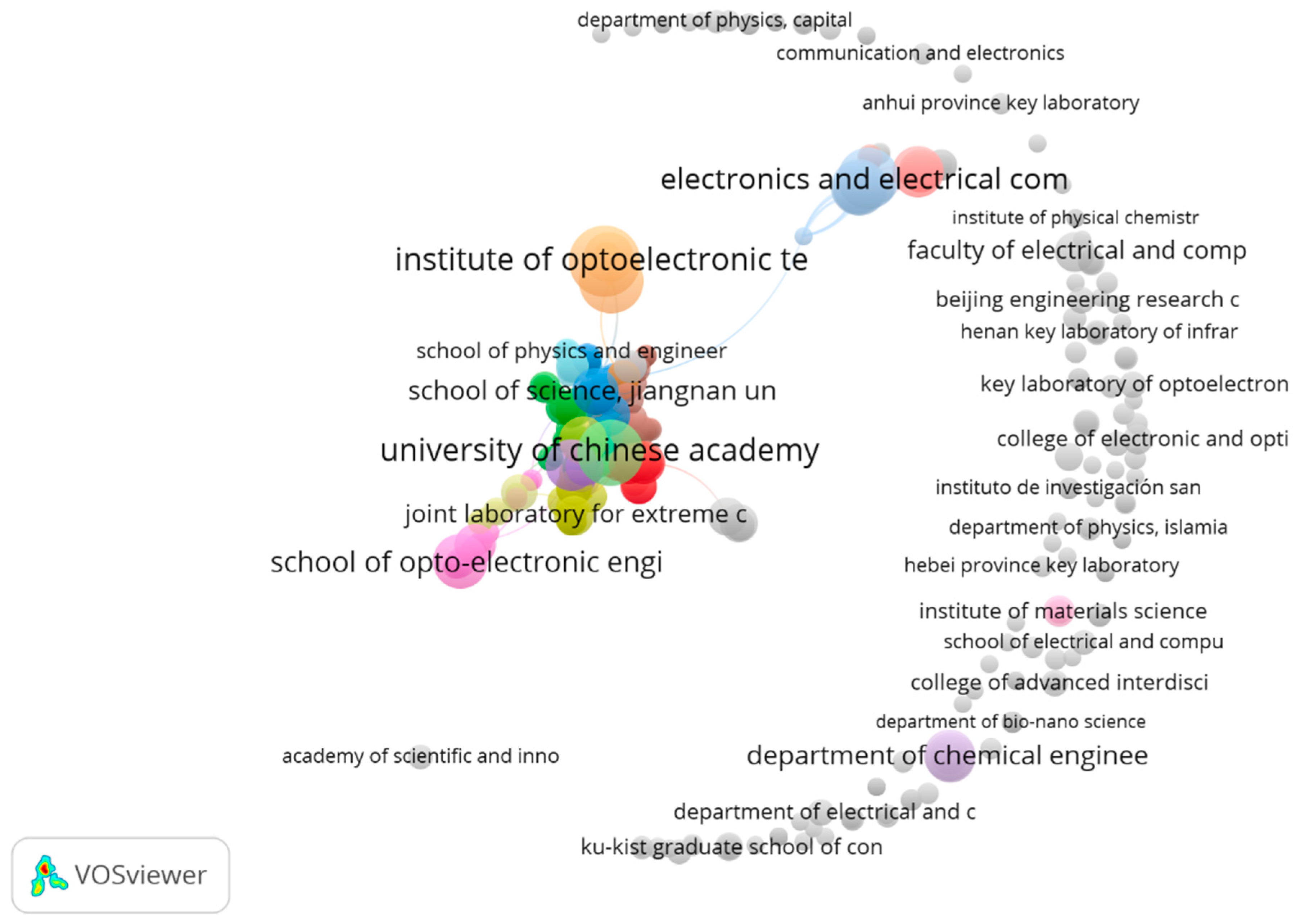
2.1.2. Institutional and Country Analysis of Metasurface Optical Biosensors

A cooperative analysis of the countries in VOSviewer is shown in Figure 4. This network graph helps us to understand the distribution of the research potential in this field. A total of 82 countries are publishing in this field, divided into nine different clusters, having a total number of links of 904 and total link strength of 4466. It can be concluded from the map that China is the largest among all countries, showing the dominance of China in the field of metasurface optical biosensors. The top 10 publishing countries are presented in Table 2. It can be seen that China dominates in this field, with a total published document count of 2908 and having 126 citations, but the total link strength is 594, showing the collaboration among researchers. The United States also has 827 documents with more citations than China at 1786; it is followed by India, with 513 documents having 51 citations. Similarly, different institutions or organizations can also be analyzed, as depicted in Figure 5.
It can be seen that the Institute of Optoelectronics China, followed by the University of the Chinese Academy, is the most productive institute, publishing more research articles when compared with other organizations around the world. Table 3 provides the predominant institutes in the field of metasurface-based optical biosensors, which are contributing heavily to research related to metasurface-based optical biosensors.

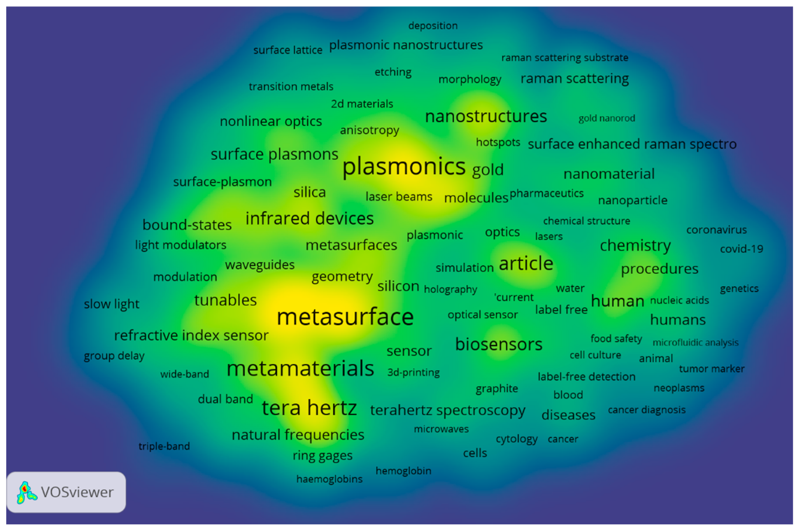
2.1.3. Co-Occurrence Keyword Analysis

The co-occurrence keyword analysis in the research field of metasurface-based optical biosensors is depicted in Figure 6. Here, the larger the font of the keyword, the greater its emphasis in the field. The top keywords in this field are metasurface, biosensors, plasmonic, metamaterials, and terahertz, which the researchers have taken as the foci of their investigations. On the other hand, the density visualization is depicted in Figure 7, also showing the main foci of researchers in this field.

2.1.4. Source Citation Analysis

The distribution of source journals that are published in this domain is depicted in Figure 8. It can be concluded that Optics Express has published the largest number of articles based on metasurface optical biosensors. Table 4 presents the top 10 journals according to the total number of published articles in this field. It can be summarized that Optics Express is the leading journal, with 325 documents, followed by the Institute of Electrical and Electronics Engineers (IEEE) Sensors journal and Advanced Optical Materials, with 151 and 148 documents, respectively. Furthermore, the percentage count can be calculated from 5844 articles, which shows the dominance of Optics Express, with 5.56% of the total articles in this field.

2.2. Principles of Metasurface Biosensing in Optical Frequency Domain

Optical biosensing has been revolutionized through two-dimensional arrays of engineered nanostructures known as metasurfaces. With precise control over subwavelength light–matter interactions, the sensitivity and selectivity can be enhanced in biological molecule detection [26,27]. The surface is composed of metal or dielectric nanoelements of gold, silver, silicon, or titanium dioxide. They are specifically prepared as resonators with forms and sizes that allow the occurrence of resonant modes: SPR in metals and Mie resonance in dielectrics [28]. Such a design enables metasurfaces to control the phase, amplitude, and polarization with the precision of incident light to optimize interactions with biomolecules, making them beneficial for advanced biosensing applications. Biomolecules, including proteins, carbohydrates, and nucleic acids, are essential components of biosensors, which are analytical instruments used to detect particular analytes; these include cholesterol, urea, penicillin, ethanol, and others [29,30,31]. A transducer, along with a tool for the analysis of data, is another essential component of a biosensor. A biosensor can be classified as either piezoelectric, acoustic, magnetic, electronic, optical, or electrochemical, depending on the transducers that are employed [32,33]. Through their quick, sensitive, and selective assessments, optical biosensors have given biotechnology, environmental research, disease diagnostics, and medicinal applications a significant advantage. The four main phases of biosensing are depicted in Figure 9, where the first phase begins with biological samples (such as blood, saliva, urine, or tissue extracts) that might include infections, biomarkers, or particular compounds of interest. These are gathered during the initial stage. The target analyte must next be extracted or separated from the intricate biological matrix by implementing techniques such as filtration, centrifugation, and chemical separation in the second step. Furthermore, the biosensor uses certain detection technologies, such as optical, electrochemical, or plasmonic sensing, to identify the target biomolecule; in the final phase, by using software, the detected signal can be processed, examined, and transformed into useful data that provide insights into the presence, concentrations, and behavior of the target biomolecule [34,35].
Traditional biosensors mostly rely on biochemical interactions, which include enzyme–substrate or antibody–antigen reactions, to detect target analytes. Although they have a high degree of selectivity, diffusion-limited mechanisms can cause prolonged response times, and signal transduction systems frequently restrict their sensitivity. Electrochemical deoxyribonucleic acid sensors and enzyme-based glucose sensors are two examples that are frequently employed in genetic analysis and medical diagnostics. Their dependence on biological components, however, may result in increased expenses and difficulties with scalability. Metasurface-based biosensors, on the other hand, greatly improve the sensitivity and response times by manipulating light–matter interactions through nanostructured surfaces. These types of sensors detect biomolecules with extremely high precision by using plasmonic and electromagnetic field confinement phenomena. For example, metasurface-enhanced surface-enhanced raman spectroscopy (SERS) has rendered molecular fingerprinting possible for disease diagnostics, and plasmonic metasurface sensors have demonstrated remarkable efficacy in biomarker identification.
The biosensing component or analyte may be a protein, aptamer, enzyme, antibody, etc. Usually, a transducer is used for the measurements, and the data are then analyzed [36]. Since optical biosensors employ an optical measurement technique, an optical transducer is distinct from other biosensors [37,38]. The optical biosensor completely integrates the biosensing element into the optical transducer. These optical biosensors’ fundamental working principles, and, consequently, their primary performance indicators, differ significantly depending on the optical transducer that is employed. Metasurfaces utilized for sensing applications are developed based on the concept of the significantly increased near field that arises from resonant electromagnetic modes near the structures [39,40,41]. The resonance characteristics, such as the frequency, amplitude, and phase, will be altered in response to variations in the refractive index ( μ ) when biological molecules are exposed to the metasurface sensor. Four major key performance indicators, namely the quality factor (Q-factor), figure of merit (FOM), sensitivity (S), and limit of detection (LOD), are used to describe different metasurface-based optical biosensors [42,43].
The parameter S may be defined either by amplitude variations or frequency shifts resulting from variations in the refractive index, as given in Equations (1) and (2), where Δ F is the frequency shift and Δ I is the change in the resonant intensity [18,44].
S = Δ F / μ
S = Δ I / μ
Similarly, the Q-factor is defined as the ratio of the central frequency ( F 0 ) to the full width at half maximum (FWHM) of the resonance spectra and can be written as Equation (3):
Q = F 0 / F W H M
Another crucial parameter used to specify the sensor’s responsiveness to minute variations in the refractive index is the FOM. Under intrinsic losses, the FOM is typically low for plasmonic planar metal structures; however, for metastructures, the intrinsic losses may be minimized by employing other materials and structures, as defined in Equation (4). The fourth sensing parameter, the LOD, is mostly influenced by the noise level and sensitivity. One way to express the correlation between the LOD and ( S ) is through Equation (5):
F O M = S / F W H M
L O D = m σ b l a n k S
Here, m is defined as a numerical factor, and σ b l a n k is the standard deviation related to blank measurements. Since the sensitivity and noise level are the primary determinants of the LOD parameter, detectors with low noise characteristics and light sources may be beneficial.
Electromagnetic radiation comprising wavelengths between 10 nm and 103 μm, or frequencies between 300 Gigahertz (GHz) to 3000 Terahertz (THz), is the standard definition of the optical spectrum [45,46]. Furthermore, the target analyte and its associated receptor on metal surfaces can be detected and their binding events studied under these biosensors. SPR employing surface plasmon polarization (SPP) is the foundation of the plasmonic biosensor. They can offer extremely low detection limits exceeding 10−5 refractive index units (RIU) because of the resonant photon and SPP coupling scenarios [47,48]. Optocouplers (i.e., prisms and gratings), which have a limited operational range and short detection distance, are necessary for SPR-based systems. This makes integrating low-cost, high-throughput capabilities and real-time biochips for the quick bioanalytical evaluation of small samples challenging at times. Consequently, biosensors based on SPP enhance the sensitivity for tiny analytes’ detection in the direction of nanoscale design and modify biochemically specific nanostructures according to their size at the nanoscale. Additionally, the optical range of frequencies can be further subdivided into the optical regime and the near mid-infrared. Due to their excellent performance and energy augmentation whenever electromagnetic waves or incident light are present in the visible or infrared domains, a unique structure known as a nanoantenna has emerged in recent decades [49,50]. These nanoantennas can be configured with nanoapertures and nanoelements. Platforms for sensing according to the aperture configuration are suitable for biosensing applications [51,52].
The fundamental basis of SPR- and LSPR-based metasurface biosensors is the investigation of the angle, wavelength, and phase, along with additional plasmon characteristics. The term “metasurface-based SPR” describes a type of artificial meta-atom, typically periodic, intended to control the polarization, phase, and magnitude of the electromagnetic spectrum [53,54]. The detection capability for metasurface-based SPR is simpler to construct and the signal is more stable than with the conventional prism coupling-based SPR. The damping range of a single metal nanostructure within dipole approximation is considerably fragmented by the collective mode resonance that is produced on the metasurfaces of periodic arrays using near-field and far-field coupling to produce resonance, along with a high Q-factor. For the periodic array layout with a two-dimensional (2D) grating structure, the diffraction wave may generate a tangential wave vector element supplied by the grating of a lattice vector, although the waves have impinged on a metal grating. In contrast, it is typically not feasible to excite SPP immediately at a perpendicular incidence in the context of SPR, since the wave vectors are not compatible directly. For a periodic grating layout, the SPP excitation condition is written as in Equation (6):
λ = a 0 m 2 + n 2 ε m ε d ε m + ε d
where the lattice constant is represented by a 0 ; scattering orders are given by m and n, respectively; and ε m and ε d are the permittivity of the metal and dielectric, respectively. Consequently, the above provides a positive relation between the refractive index of the surrounding medium and the resonance wavelength, establishing the necessary mechanism of biosensing for periodic metasurfaces.
Under the influence of an electromagnetic field, the resonance effect of LSPR can be considered as a metal spherical nanoparticle having a radius a such that ( a λ ) [55]. The resonance frequency ω l of LSPR can be determined by combining the metal Drude mode expression with the Laplace equation together with a boundary condition, subsequently disregarding the damping effect, as given in Equation (7):
ω l = ω P l ε d l + 1 + l 1 / 2
where ω P denotes the plasma frequency, ε d is the permittivity of the environment, and l denotes the angular momentum for the resonating mode.

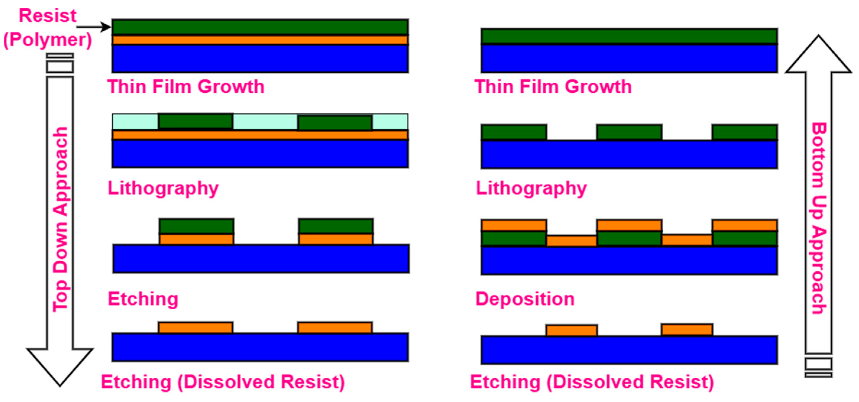
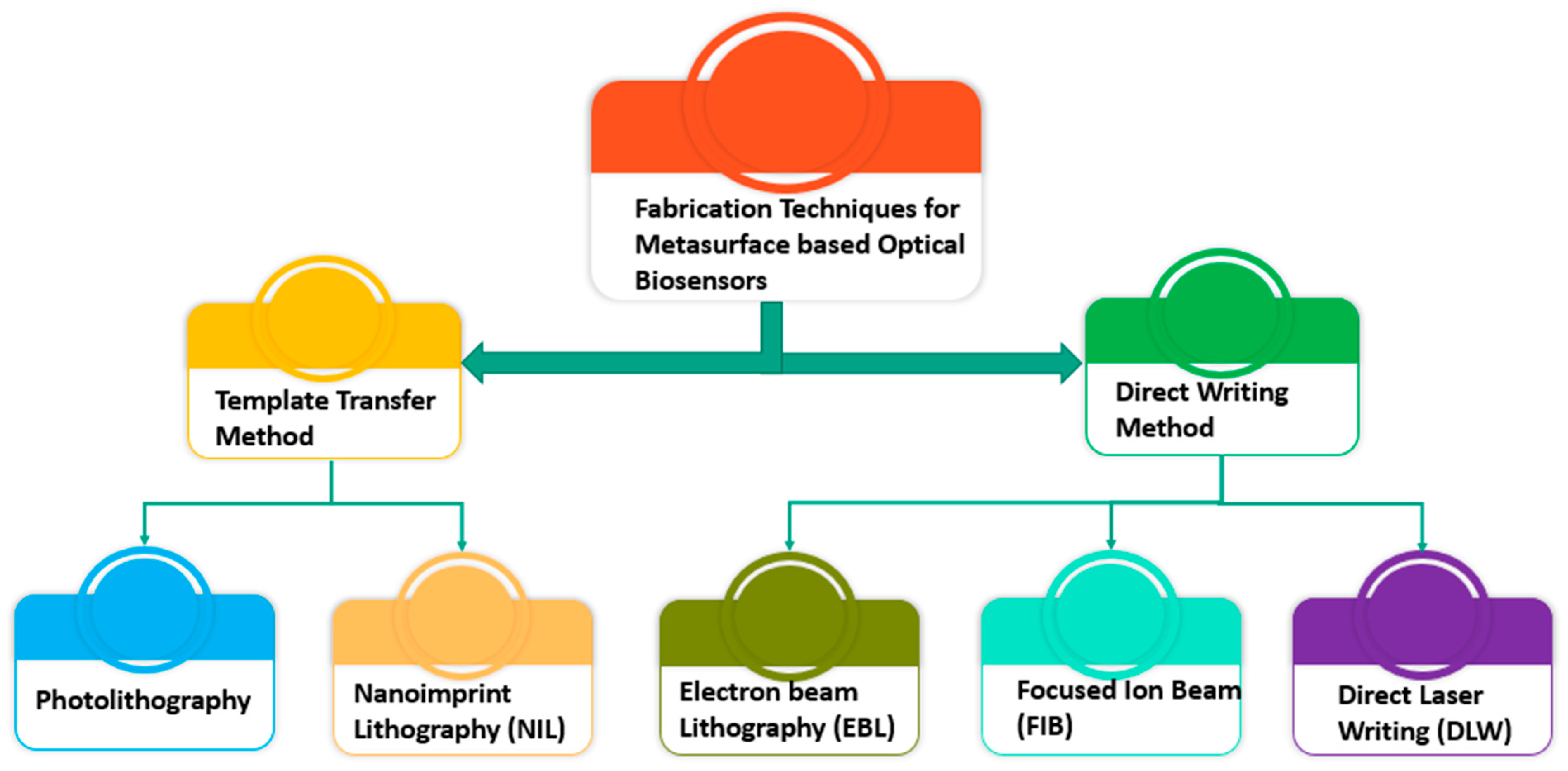
3. Advanced Fabrication Techniques

Both top-down and bottom-up techniques are used to create micro-/nanostructures for the fabrication of metasurface-based optical biosensors. The bottom-up approach is initiated by thin layers of deposited or evaporated material along with lift-off procedures to create micro-/nanostructures from scratch [56]. The top-down method produces nanostructures through etching or imprinting a small portion of a large entity, as depicted in Figure 10. Both methods are utilized in the production processes of complex multilayer structures for the chip industry. For the single-layer metasurface, the choice of top-down and bottom-up approaches is much simpler. The most challenging aspect is to produce complex 2D designs [57]. The rest of this section classifies and elaborates on typical pattern processing techniques for the fabrication of optical biosensors using metasurface structures, as depicted in Figure 11.

3.1. Template Transfer Methods

In nanofabrication, template transfer techniques are essential because they allow for the high-resolution, scalable, and economical patterning of nanoscale systems, specifically for metasurfaces in optical biosensing. Molds are used in processes like soft lithography along with nanoimprint lithography (NIL) to create or transfer patterns upon substrates, making them suitable for large-scale production with nanoscale accuracy [58]. Nanostructures can be applied to non-traditional surfaces, which include flexible or curved ones, using techniques like transfer printing along with electrochemical deposition. Furthermore, versatility is provided by the lift-off technique along with capillary force lithography (CFL), which may create complex shapes in a variety of materials. When combined, these techniques enable a wide range of applications, including nanophotonic devices and biosensors.

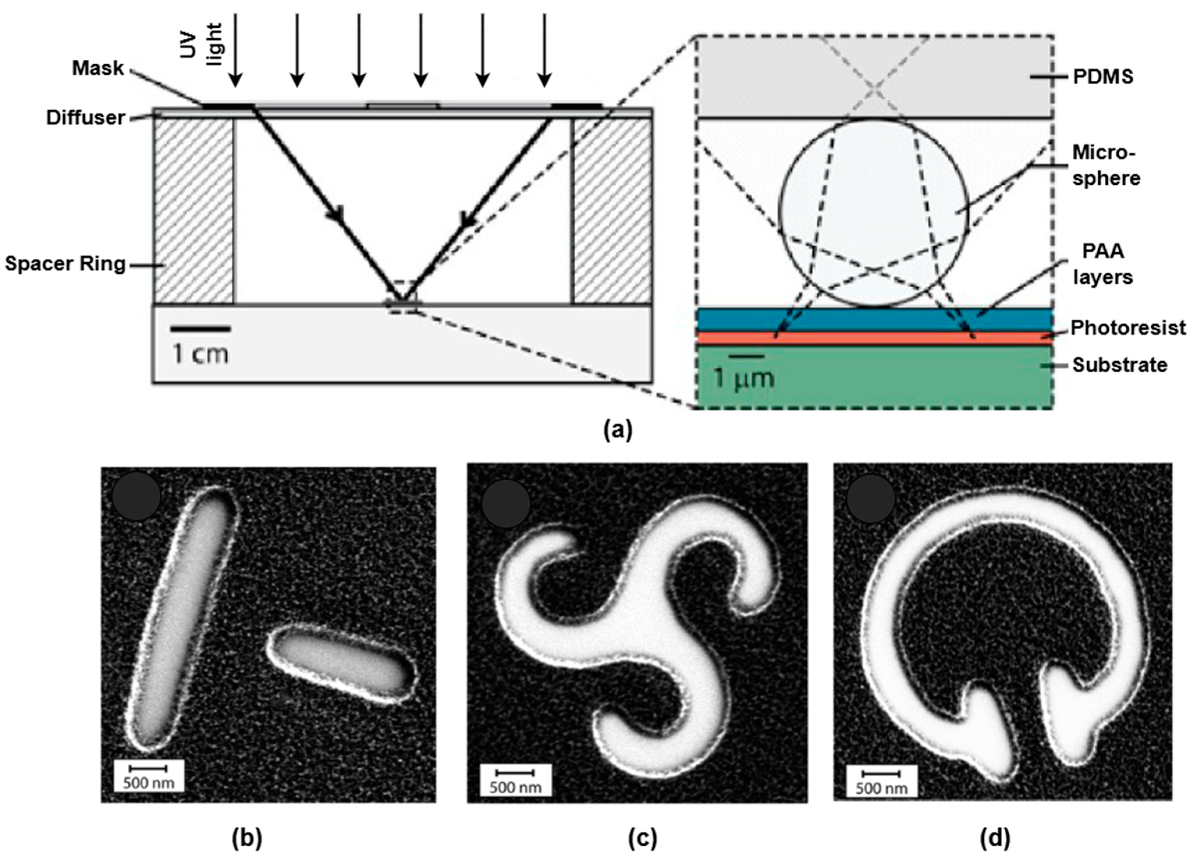
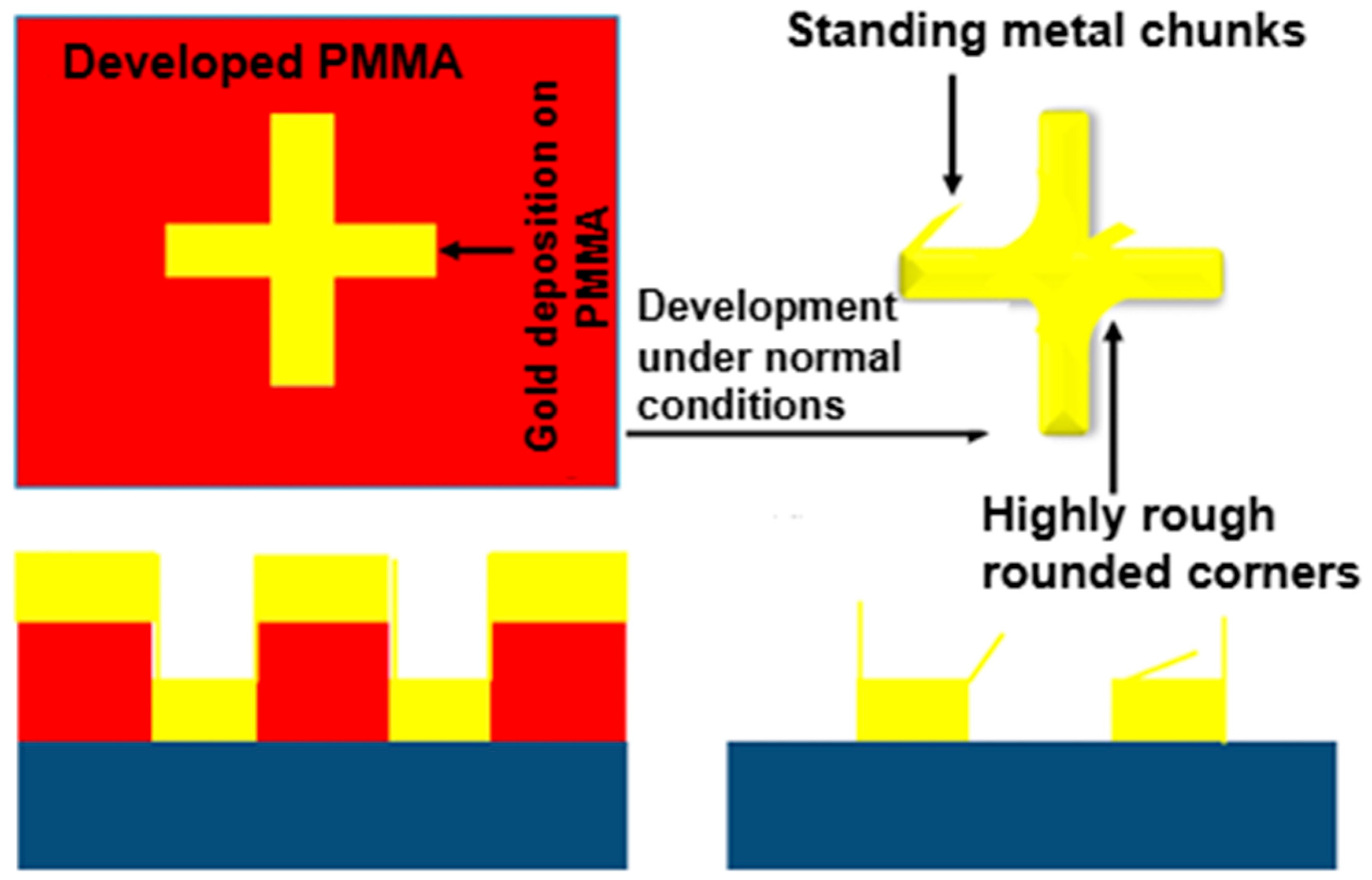
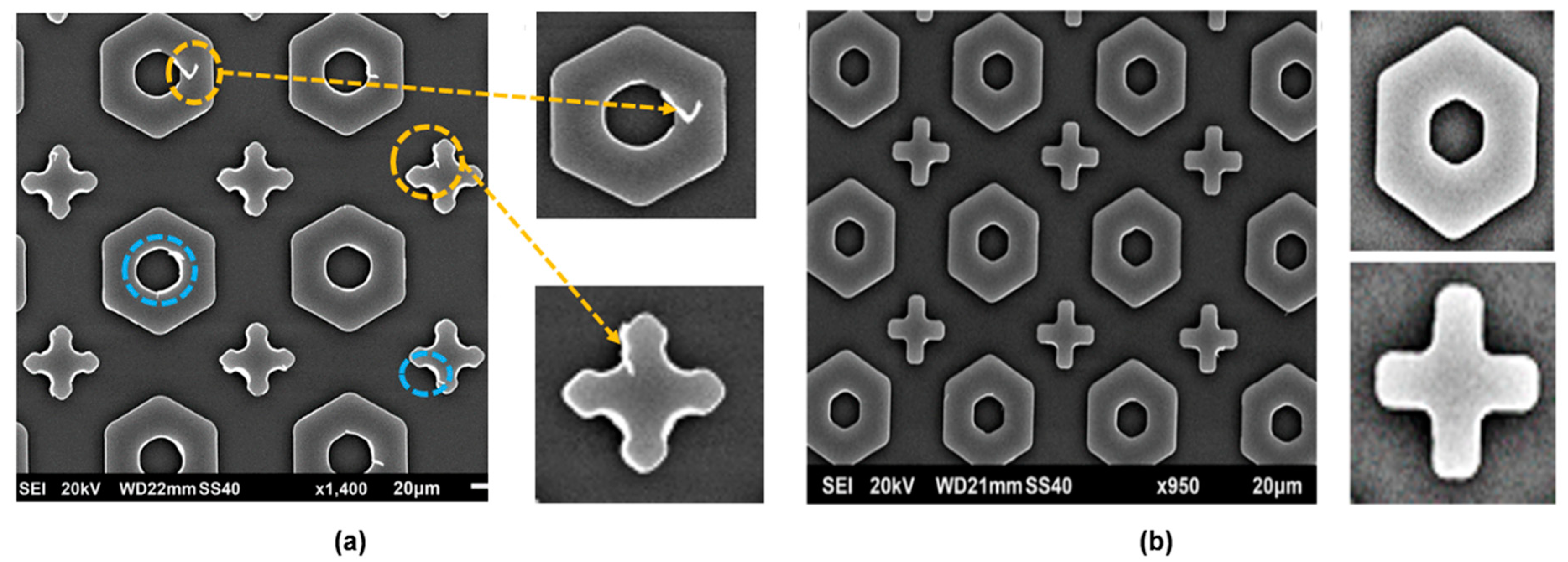
3.1.1. Photolithography

A silicon-on-quartz substrate is usually used to create micro/nano metasurfaces. A thin layer consisting of a metal or dielectric material is then produced using chemical vapor deposition (CVD) or even physical vapor deposition techniques. Photolithography, invented in 1959, can then be used to transfer the intended pattern, while development and etching procedures can be used to remove extra material [59,60,61]. As a substitute, photolithography or self-assembly techniques can be used to create pre-patterned photoresists or expendable layers on the substrate. After the materials have been laid down, a lift-off procedure is used to eliminate the excess material, including the sacrificial layer. This group of highly developed micro/nano processing methods is widely used in the production of semiconductor chips. The etching and projection photolithography procedures are two of the most important phases in this procedure. In projection photolithography (PPL), incoming light and photoresists combine to transfer geometrical patterns from a photomask to a substrate. During scanning, ultraviolet light travels across the photomask and strikes the photoresist layer [62]. After chemical reactions, the photoresist in the region of exposure is removed by employing development technology, enabling additional pattern fabrication on the substrate utilizing etching and deposition approaches.
The photoresist in the exposed area (positive resist) alongside the unexposed area (negative resist) is subsequently eliminated. Plasma etching and dry etching techniques, like reactive ion etching and deep reactive ion etching, are often employed for etching. To create non-periodic metasurfaces, a microlens PPL technique was proposed by Mathieu Gonidec et al. [63] for the creation of infrared metasurfaces, which offer new possibilities for the quick prototyping of periodic and quasiperiodic metasurfaces, especially those using feature sizes between 0.4 and 10 μm. This technique combines the ease of self-assembly with the accuracy of projection lithography. It allows for quick iteration between several unit cell designs, instead of requiring a high-resolution master, to create an array of microspheres that correspond to the intended distribution of characteristics, as depicted in Figure 12. An illustration of the setup for projection lithography is depicted in Figure 13a. A centimeter-scale photomask is illuminated by a strong source of noncollimated ultraviolet (UV) light, which is transferred onto the underlying photoresist to replicate the mask’s characteristics. Scanning electron microscope (SEM) images of three samples with a T pattern lattice, chiral triskele pattern, and split C resonator pattern are depicted in Figure 13b,c,d, respectively. Template PPL makes it possible to quickly and affordably fabricate huge area arrays of randomly positioned nanostructures without the need for specialist equipment. The smallest feature size that could be achieved with the microlenses employed was about 0.4 μm while utilizing an unfiltered UV source. PPL facilitates the creation of both periodic and non-periodic topologies and the effective investigation of how the lattice structure affects the optical characteristics of infrared metasurfaces.

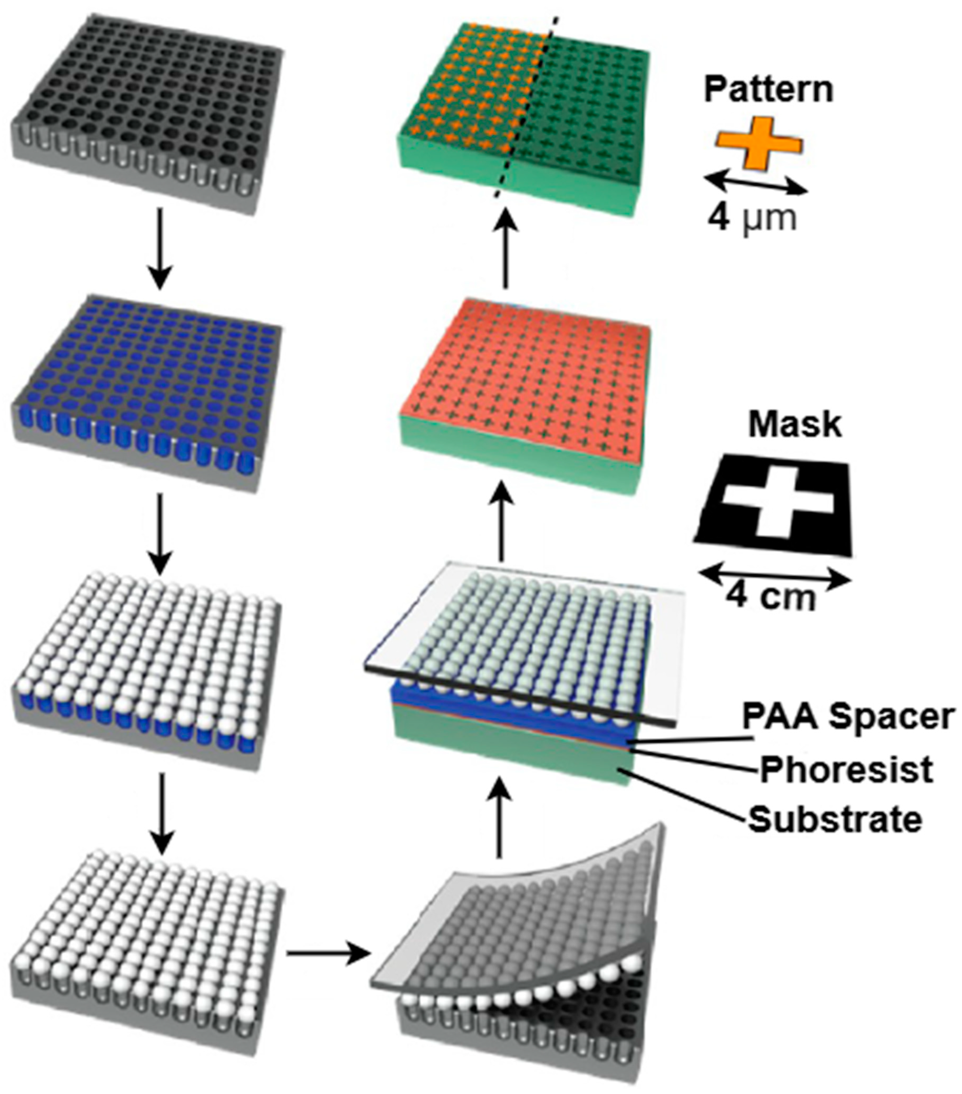
3.1.2. NIL Technique

A method invented in 1995, called NIL, replicates nanostructures by utilizing mechanical deformation. Its benefits include efficiency and affordability, large-area processing, and outstanding resolutions (10–100 nm). However, high-resolution technology is required for the manufacturing of the template (mold). Thermal and UV embossing are components of traditional NIL [64]. Lower-viscosity materials with elevated temperatures are used in thermal embossing. After the template is pushed into the polymer-coated substrate, the polymer is heated and cooled to harden it. The NIL pattern is transferred to the substrate following template separation, and then further etching and polymer elimination procedures are carried out. Using UV light to cement the polymer layer throughout the imprinting process, UV embossing is performed at room temperature. It typically boasts greater production because of its simple system and quick reaction time. Furthermore, a type of thermoplastic polymer resin that has been placed on a substrate is pressed upon by an imprint mold during thermal NIL [65]. To soften the plastic resin and enable it to follow the layout of the mold, this technique demands both heat and pressure. Following the imprinting of the desired pattern, the mold is removed, retaining the patterned resin upon the substrate, and the entire process is cooled down to solidify the resin. Because this technique depends on high temperatures, it works well with materials that can withstand heat but is less appropriate for applications where the temperature is a determining factor. On the other hand, UV NIL uses a photopolymer resin within a clear imprint mold. This technique applies pressure while curing the resin with UV light rather than heat. There is no requirement for cooling before mold detachment because the photopolymer solidifies when exposed to UV light at ambient temperature [66]. Because there are no heating or cooling stages, this room-temperature method is typically faster than thermal NIL and is useful for scenarios wherein thermal effects must be reduced. Given the above, UV NIL provides a quicker, room-temperature option for UV-sensitive materials, whereas thermal NIL is more appropriate for applications needing great durability.

3.2. Direct Wiring Methods

Considering that direct writing techniques offer the accuracy and adaptability required to produce nanoscale patterns that influence light at certain wavelengths, they are very useful for the fabrication of metasurfaces for optical biosensors. Because they enable incredibly high-resolution features, which are necessary in regulating optical properties, electron beam lithography (EBL) [67], direct laser writing (DLW) [68], and focused ion beam (FIB) lithography [69] are a few examples that are especially helpful in producing the complex nanoscale patterns needed in the fabrication of metasurfaces. By precisely eliminating material to create the desired structures or altering a substrate’s optical characteristics, DLW can also be used to fabricate metasurfaces for sensing applications. Rapid iteration in the creation of biosensors is made possible by the speedy prototyping and production of unique designs via inkjet and 3D printing techniques [70,71,72,73]. The electromagnetic characteristics of metasurfaces may be modified using these direct writing techniques, which makes them suitable for improving their specificity and sensitivity in optical biosensing applications.

3.2.1. Electron Beam Lithography (EBL)

EBL, invented in 1960, is a fabrication technique that does not use a photomask to set up the pattern. It entails directing a concentrated stream of electrons with extremely short wavelengths across an electron-sensitive photoresist. The EBL technique provides flexible drawing (allowing direct writing without additionally using a mask) and an ultra-high resolution (reaching an extreme component size of <10 nm) [74,75,76,77]. EBL is now the most popular technique for the creation of metasurface-based optical sensors because of its excellent resolution and significant degree of freedom, aligning well with the processing needs of regularly or non-periodically ordered micro-/nanostructures. The disadvantage of this maskless lithography technique is that it takes a long time to create intricate large-area designs, which leads to a low yield. Its current uses are mostly restricted to the production of masks and the research and development phases of devices. Al Hasan et al. [78] reported a substantial area of metasurface development using the EBL approach to create cross-shaped metasurfaces and hexagons having uniform corners. This technique produced high-resolution and high-quality metasurface prototypes by defining precise patterns upon polymethyl methacrylate (PMMA) resists, regulating the proximity effect, and ensuring the appropriate exposure dose, as depicted in Figure 14. According to the characterization findings, metasurfaces with consistent metal corners achieved stronger absorption and higher field improvements at long wavelengths in the infrared spectrum. The metasurface created using the first approach utilized a PMMA resist upon a silicon substrate comprising a 10 nm chromium layer subjected to 20 keV, particularly with 200 µC/cm2. It was developed for 120 s at 22 °C in the solution. The resulting SEM image, depicted in Figure 15a, showed the cross-shaped absorber’s rough corners with rings. Meanwhile, a metasurface was created with polyethylene furanoate (PEF) with a controlled proximity range, which produced a higher-quality metasurface (450 µC/cm2, 50 keV). The formation was obtained at 22 °C after dipping it in the developer solution for 60 s. The cross-shaped and hexagonal metasurfaces both had delicate corners along with sharp edges, as depicted in Figure 15b.

3.2.2. FIB Technique

FIB is another high-resolution, maskless, direct writing process, developed in 1975. Through the application of an ion beam that bombards the target surface without any kind of photoresist, this technique removes atoms from the surface to produce patterns. FIB may theoretically be applied to any metal or non-metal due to its entirely mechanical processing, which eliminates the need for material selectivity [79,80,81,82]. In this process, both the etching depth and width are comparatively large due to the employment of larger ions. Additionally, gaseous precursors might be bombarded by the ion beam, leading to material disintegration and direct deposition onto the sample surface. This gives FIB the ability to be used in both top-down and bottom-up approaches. Because of its remarkable degree of freedom, FIB may additionally be employed for micro-/nanomanufacturing on targets’ rear sides or rough faces. A unique metasurface was produced by Z. Liu et al. using a straightforward closed-loop nano-kirigami technique based on the continuous shape alteration of a floating ultra-thin gold film having a thickness of 8 nm [83]. Because of the interactions that occur between the induced electric and magnetic moments, it is easy to build pinwheel-like metasurfaces with 3D twisting features that have significant polarization conversion along with handedness-sensitive phase characteristics, as depicted in Figure 16a–f.

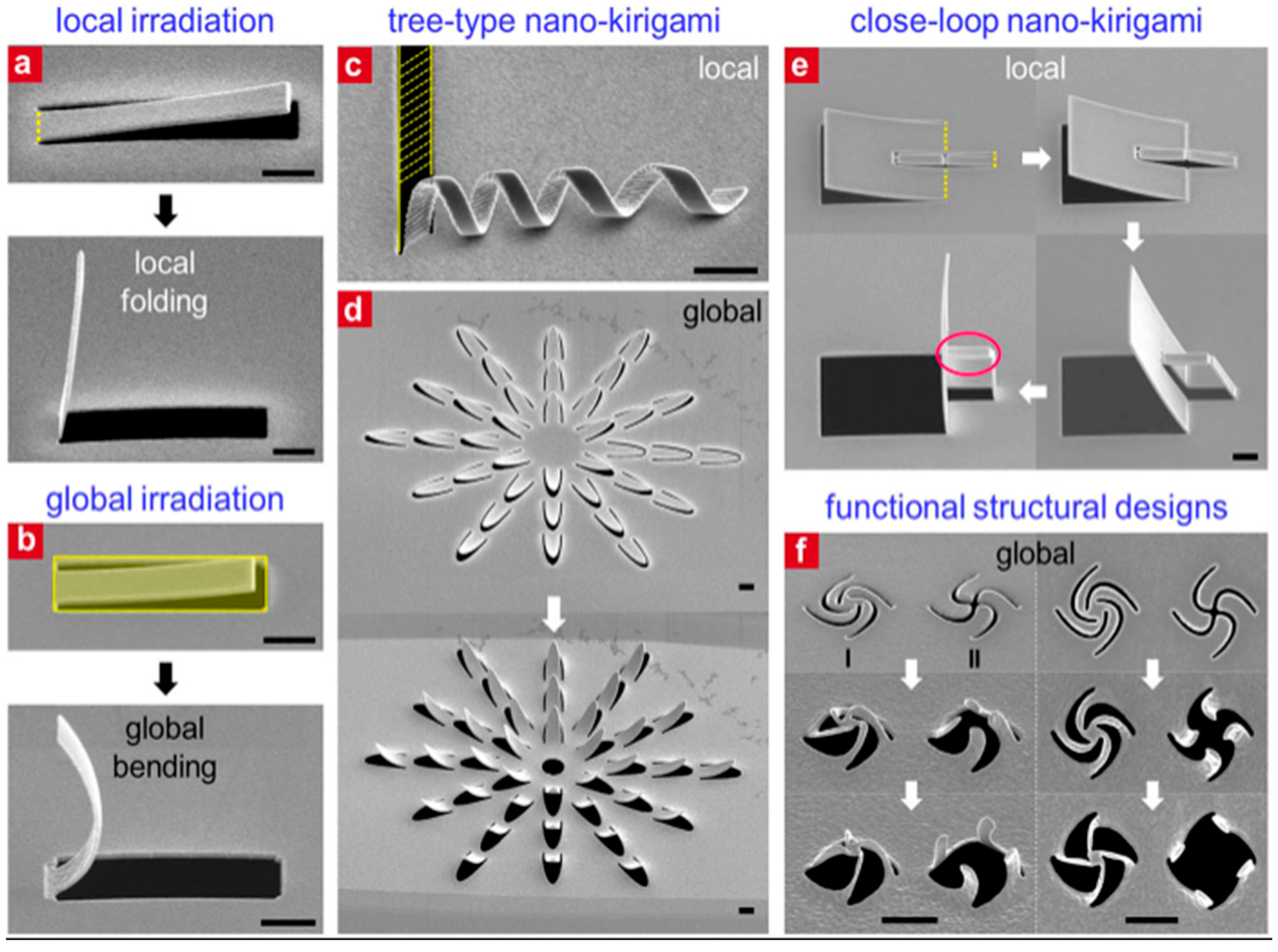
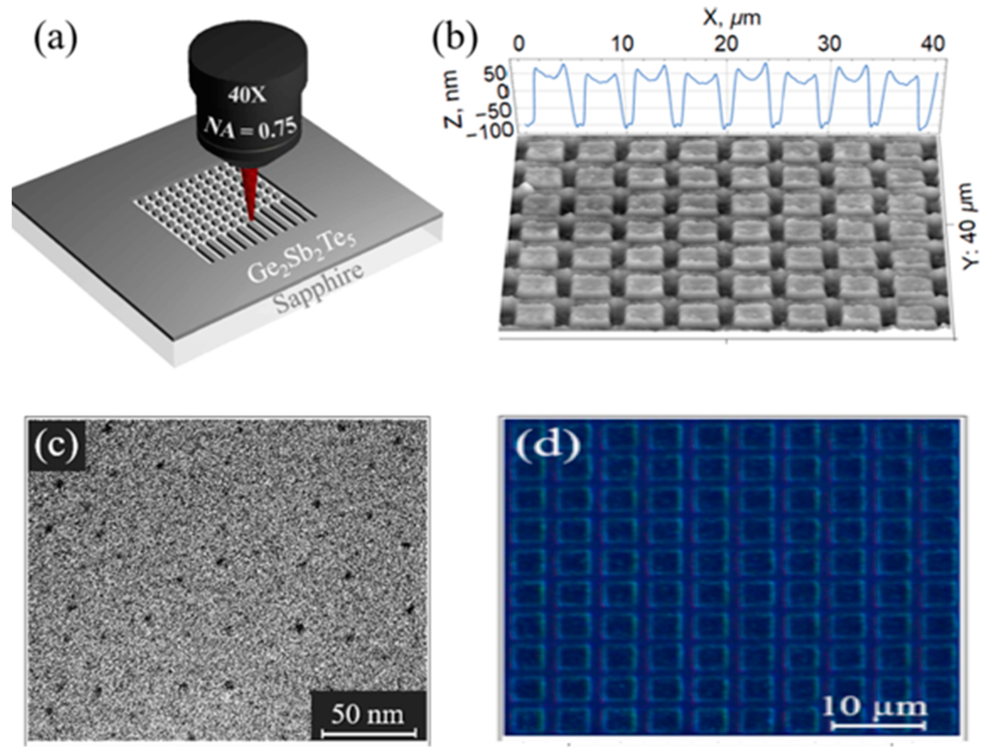
3.2.3. DLW Technique

The DLW method, developed in the early 2000s, uses laser beams to scan along and process materials directly. It has the benefits of being maskless, extremely flexible, and affordable and processing materials very quickly. DLW can be further divided into two direct printing technologies, continuous and ultrafast laser direct writing, depending on the material processing techniques applied. To create the necessary patterns, direct laser writing uses a laser beam with an adaptable intensity that scans the exposure to the photoresist. The designs are then built on the substrate via etching. Nevertheless, the optical diffraction limits the resolution of DLW processing, limiting its use to terahertz waves (760 nm to 3 mm) and infrared [84,85,86]. To minimize photothermal effects and possible deterioration, ultrafast laser direct writing interacts with materials in only a short period that is much smaller than the thermal relaxation time of the material. However, by using ultrafast light pulses at femtosecond levels to accomplish polymerization in any region of a photosensitive material, this printing technique takes advantage of the properties of such materials. With a resolution of 100–200 nm, this technique can define features that are smaller than is possible with traditional single-photon polymerization. It can create materials that are difficult to process mechanically and enable 3D printing because of the two-/multi-photon absorption characteristics and abundant radiation [72,87,88]. The processing of devices featuring more intricate or even three-dimensional architectures can also benefit from this capacity. However, the resolution of DLW is somewhat lower than that of the previously described technologies. Nonetheless, it still provides the benefits of marginally faster processing times and lower processing costs. A metasurface consisting of germanium (Ge), antimony (Sb), and tellurium (Te), also known as GST, with a period of 3 μm, was produced by the Bochek et al. [89] by utilizing the DLW fabrication technique. In this fabrication method, the laser electrodispersion approach was used to create the GST films upon sapphire or glass substrates. This method involved using a strong laser pulse to spray submicrometer droplets away from the target surface, followed by their cascade fission. Polycrystalline GST, which was created by combining elements such as Ge, Sb, and Te, was used to create the targets. The authors employed an Nd:YAG laser with a 1064 nm wavelength and a 30 Hz pulse repetition rate, along with a 1 mm spot diameter. Sapphire and glass were the two types of substrates employed for this fabrication. Parametric comparisons were performed based on three different techniques, namely atomic force microscopy (AFM), SEM, and transmission electron microscopy (TEM), for the constructed structures, as depicted in Figure 17a–d.

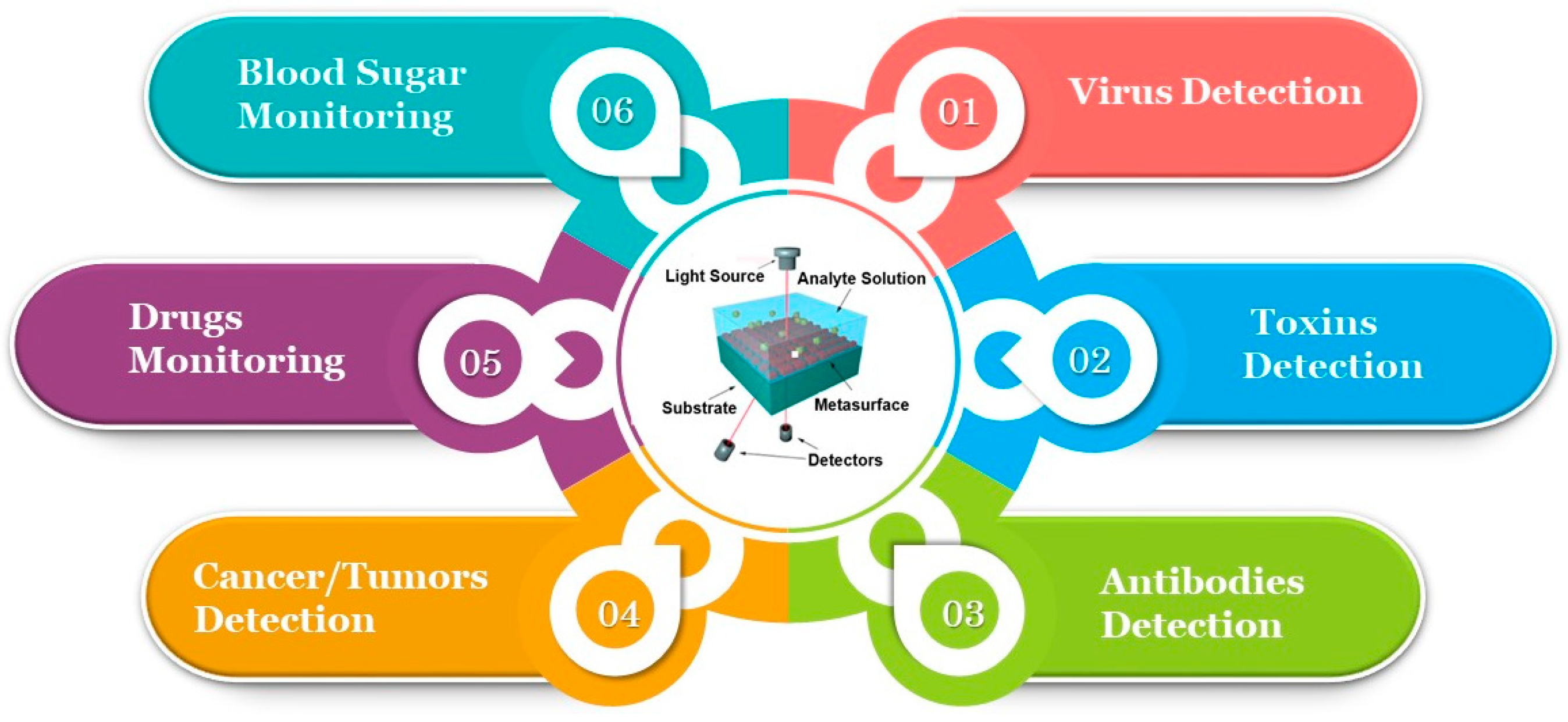
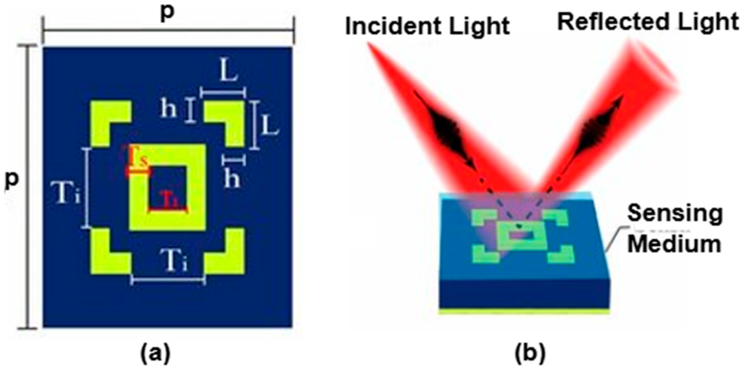
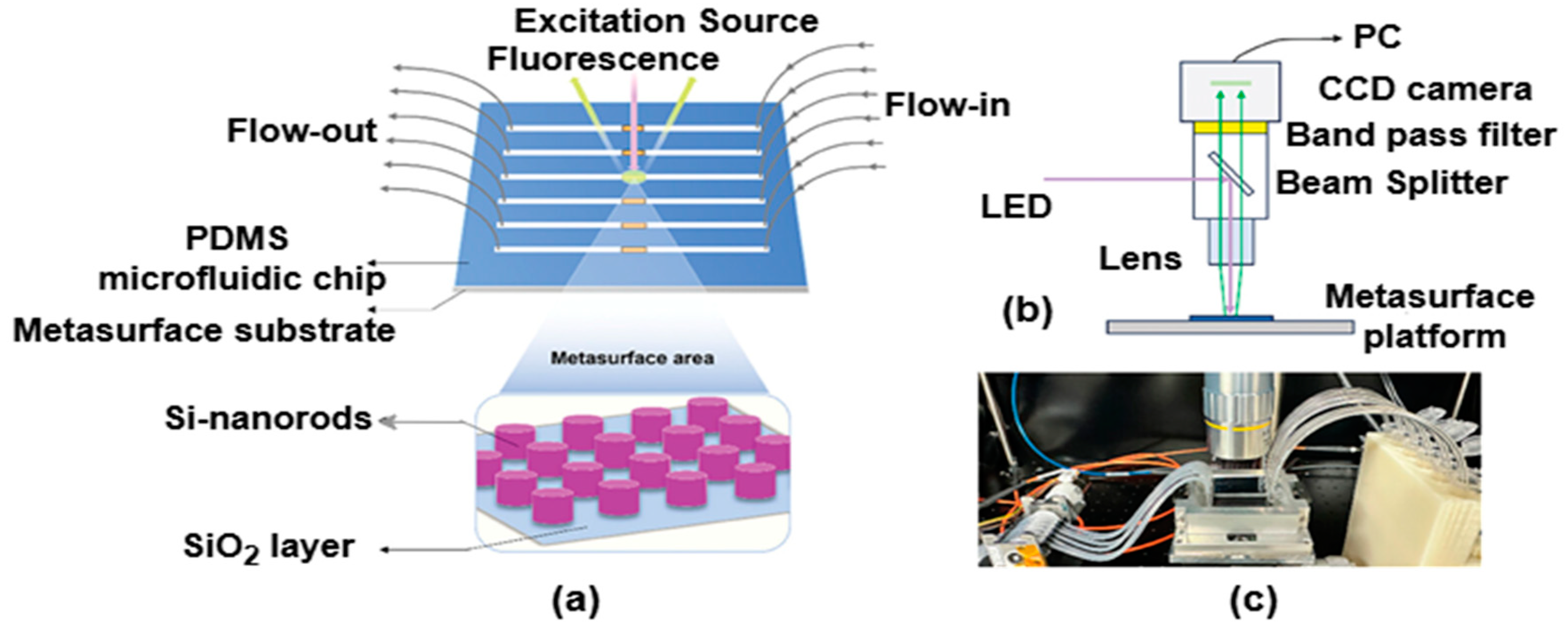
4. Parametric Analysis of Metasurfaces Enabling Optical Biosensing Applications

This section delves into a comparative evaluation of different metasurface biosensors and draws attention to how the structural design, fabrication techniques, and material selection affect the performance of a biosensor. Commonly utilized materials with distinctive optical characteristics that affect the sensor’s sensitivity, and robustness, along with the resonance behavior, include silicon, gold, and other dielectric compounds [90,91]. Furthermore, parametric investigations that focus on structural features like the unit cell thickness, periodicity, and shape demonstrate how these traits affect important metrics, such as the field enhancement, Q-factor, and resonance shifts. Metasurfaces can be tailored to particular biomolecular interactions by optimizing these parameters, rendering them adaptable to a wide range of applications, including virus detection [92,93], drug monitoring [94], and tumor detection [95,96], as depicted in Figure 18. Metasurface-enabled optical biosensors are poised to revolutionize biosensing by establishing new benchmarks in precision due to their great performance and adaptability. Shobit et al. [97] investigated graphene with a metasurface designed around a gold nano-octagonal structure, presenting a novel biosensor for early cancer detection. By enhancing graphene’s optical characteristics, the metasurface greatly increased its sensitivity and selectivity. The design and simulation of a biosensor for cancer detection were reported by the authors of this work. With a detection limit of 0.328 RIU−1 and peak sensitivity of 800 GHz/RIU, the biosensor could successfully detect cancer biomarkers from human serum samples. The sensor’s remarkable resolution and FOM parameters of 0.298 and 3.789 RIU−1 demonstrate its excellent sensitivity and specificity in detecting minute fluctuations.
The graphene layer is located in the center, providing a central circle with a 0.34 nm thickness and a material composition of pure graphene. The exterior nickel-coated octagonal framework, which is 50 nm thick, envelops the graphene layer. The outside circle, which is composed completely of gold, extends from the inner core. This outer circle has a 50 nm two-dimensional display. The glass substrate offers a sturdy base for the entire structure. The thickness of this substrate is 1500 nm. The thickness of the analyte, primarily consisting of cancer biomolecules, is maintained at 1500 nm. However, in another work on the detection of cancer, Shobit et al. [98] proposed four different metasurface sensor layouts developed for the detection of various cancer-affected cells, including a metasurface design with no gaps (MSDG), a metasurface design with outer gaps (MSDG1), a metasurface design with inner gaps (MSDG2), and a metasurface design with inner and outer gaps (MSDG3). When the refractive indices of the two cell types were compared, it became clear that the optical characteristics of cancer-contaminated cells differed significantly from those of their normal counterparts. It was found that 80% of a liquid sample contained cancerous cells. To obtain the best design, the structural parameters were changed. Several factors were examined for the sensors, such as the detection limit, FOM, Q-factor, absolute and relative sensitivities, etc. The highest sensitivity levels of 66.67 GHz/RIU, 66.67 GHz/RIU, 200 GHz/RIU, and 207.14 GHz/RIU were attained for each structural design, both in terms of absolute and relative sensitivity.
The best design of MSDG3 yielded a minimal detection limit of 0.17 RIU and a Q-factor and FOM of 13.11 and 3.86 RIU−1, respectively. The four different proposed metasurface-based optical biosensor configurations are depicted in Figure 19a–f.
The resilience of all-dielectric metasurface biosensors consisting of pairs of a transparent microfluidic chip and a silicon nano pellet array with enhanced fluorescence was investigated by Masanobu et al. [99] through several experiments. It was demonstrated that the metasurface biosensors performed well in identifying a wide range of targets, including proteins, antigens, and antibodies, as well as nucleic acids. The most recent findings demonstrate nearly four-order broad dynamic ranges for carcinoembryonic antigen (CEA) and prostate-specific antigen (PSA), ranging from 2 pg/mL to 25 ng/mL and 0.16 ng/mL to 1 g/mL, respectively. The clinical criteria for PSA and CEA, namely 4 ng/mL and 5 ng/mL, respectively, are within this range. These metasurface biosensors have not yet been the subject of thorough robustness verification.
Another work on the detection of cancer was reported by Mostufa et al. [100], focusing on the resonant infrared frequency of 39.8 THz. The reported L-shaped metasurface sandwich structure achieved an almost perfect absorption rate of 99.996%, exhibiting remarkable absorption capabilities. Furthermore, the researchers were able to maximize the sensor’s absorption peak by optimizing its structural properties. Optimizing the material thickness of the SiC dielectric spacer (from 0.20 to 0.45 μm), the gap between the L-shaped corners (from 0.60 to 0.90 μm), and the gold (Au) layer (from 0.03 to 0.28 μm) was considered in the design, as depicted in Figure 20a,b. It was possible to achieve a Q-factor of 10.33 and sensitivity of 3.74 THz/RIU across a broad range of refractive indices (from 1.0 to 2.0). Furthermore, it showed sensitivity of 3.5 THz/RIU for cancer diagnosis. These results demonstrate the effectiveness of this mechanism in precisely identifying variations in the refractive index.
In another application for biomarker detection, because of their quick reactions, excellent selectivity, and low background noise, fluorescence (FL) biosensors with aggregation-induced emission (AIE) characteristics have shown exceptional performance in biomarker identification. Nevertheless, because complex urine samples contain a variety of uncontrollable variables, such as contaminants, autofluorescence, other urine components, etc., it is challenging to identify extremely low-level analytes in real-world applications. To address such interference in the context of human urine, increasing the optical signal sensitivity for human serum albumin (HSA) detection is necessary.
The authors Qi Hu et al. [101] proposed biofunctionalization procedures on silicon nanostructures to quantitatively detect trace HSA in urine using an AIE-based FL biosensor consisting of tetraphenylethylene (TPE)-4TA in conjunction with an all-dielectric metasurface framework. The findings showed a notable FL improvement in the metasurface platform, which presents a viable avenue for further biomarker detection advancements. AIE-characterized FL biosensors in conjunction with nanophotonic all-dielectric metasurface platforms provide improved HSA detection. As illustrated in Figure 21a, this platform combines a microfluidic system with a metasurface substrate to facilitate analyte delivery and the instantaneous monitoring of FL enhancement. Its exceptional features include high throughput, superior reusability, and low reagent usage. The findings from human urine samples taken under the FL arrangement shown in Figure 21b,c demonstrate the great potential of the reported metasurface as a biomedical chip-based framework, offering a promising avenue for improved sensing and quantitative biomarker identification. The findings show strong photostability with an excellent dynamic range of 0–160 μgmL−1, indicating that it is particularly sensitive to detectable HSA. Additionally, across the three platforms, the findings of urine testing show a significant FL retention rate of 9%, the lowest LOD (18.75 ngmL−1), along with the best recovery rate (96%) in urine that is up to 2560 times diluted.
Another work on the real-time monitoring of biomolecules like glucose or hemoglobin was performed by Ghulam Khan et al. [102]. They used a metal–dielectric–metal combination consisting of silver square block arrays (SSBs) to concurrently obtain a high quality factor and increased sensitivity. A wide range of biomolecules could be detected. The suggested design supports three modes that arise from gap plasmons, including propagating SPR. Significant sensitivity was shown by the proposed sensors in various modes: keeping the quality factor of Mode I equal to 17, Mode II equal to 356, and Mode III equal to 107, respectively, the FOM was 7 RIU−1 for Mode I, 375 RIU−1 for Mode II, and 98 RIU−1 for Mode III. The suggested sensor effectively detects varying hemoglobin and glucose concentrations, making it suitable for real-time biosensing applications. Additionally, for virus detection, Zahra Sadat et al. [103] investigated the fabrication of a fractal plasmonic metasurface with Fano resonances that was optimized to function in the near-infrared optical spectrum (2000–5000 nm). Fano resonances, as opposed to conventional plasmonic resonances, enable better sensitivity and clearer spectrum characteristics. The metasurface was composed of four smaller rings positioned in the cardinal directions, having five disks in the spaces between them, along with a main ring with self-similarly structured nanoscale rings and disks. Several electromagnetic hotspots within the structure provide this fractal-like architecture with enhanced light–matter interactions. In the future, affordable, reusable viral detection devices that can be integrated with smartphone photography and telemedicine applications may be possible with this geometry by tweaking its capabilities, in the absence of labels or dyes. Similar criteria might apply to various target analytes, even at the molecular level. Another work by Shobhit et al. [104] sought to identify COVID-19 by detecting a substantial ratio of ethyl butanoate in an affected individual’s exhaled breath. They employed a metasurface-assisted slotted T-shaped absorber in conjunction with a refractive index sensor (RIS) to detect ethyl butanoate with high sensitivity. By adjusting the structure’s length and thickness, as well as the slotted T-shaped resonator’s length, width, and thickness, the sensor’s optimal structure was achieved. A ground layer composed of gold material was first positioned to produce the structure, and then a substrate layer composed of magnesium fluoride was added. Later, the resonator layer composed of gold material and the magnesium fluoride substrate layer were separated by a graphene sheet. The highest sensitivity of 2500 nm/RIU, FOM of 131.58 RIU−1, and detection limit of 0.0224 RIU were all attained with the suggested slotted T-shaped RIS.
Additionally, Xiangbao Yin et al. [105] proposed a graphene–dielectric metasurface-based optical biosensor for the sensing of hemoglobin. The design consists of an array of asymmetric silicon bars, which is placed on a graphene sheet to form the metasurface. The structure exhibits Fano resonance with a high Q-factor. Additionally, each silicon bar has a gap where a strong light–analyte interaction occurs, but the optical field is very limited. The metasurface’s numerous geometrical properties are tuned. This results in an FOM of up to 587 RIU−1 and high sensitivity of 392 nm/RIU. Furthermore, metasurface-based biosensors are also utilized for drug monitoring. The authors Jun Gao et al. [106] suggested using hybrid silver and gold nanostructures for a super-absorbing metasurface. Without using top-down lithography technology, a two-step technique of deposition followed by heat annealing was created to reduce the distance between the metallic nanoparticles [107]. The hybrid silver and gold metasurface structure facilitates a light trapping method that allows the excitation laser energy to be more effectively confined at the nanoparticle edges, improving the sensing resolution. However, a higher density of small nanoparticles causes more hotspots to be excited throughout a given area, which causes the more uniform spatial distribution of the localized field. This leads to better performance for the possible quantitative sensing of chemicals such as molecules with thiol groups and drugs like cocaine, with concentrations as low as 10 μg/mL. Another application of metasurface biosensors is in toxin detection in contaminated water. It is commonly recognized that copper and magnesium ions can contaminate water. They can harm humans and aquatic life in several ways and have the potential to be poisonous or cancer-causing. Numerous health issues, including headaches, nausea, vomiting, liver problems, and gastroenterological issues, are triggered by drinking water that contains copper and magnesium. Aquatic life is impacted by high copper and magnesium ion concentrations in water, and the ecology is disrupted. Industries based on copper and magnesium are the causes of contaminated water due to untreated copper. Almawgani et al. [108] investigated chemical techniques for the identification and monitoring of the existence of these potentially dangerous toxins. These techniques are limited by the intricate apparatus and time-consuming, costly, and challenging chemical procedures, despite their relatively high sensitivity and low detection limits. An efficient sensing technique based on a graphene metasurface has been proposed. A glass substrate optical sensor created from graphene metasurfaces has been developed that has sensitivity of 113.92 GHz/RIU for Cu2+ and 113.9 GHz/RIU for Mg2+. Furthermore, the linear fitting curve for each of the metal ions was determined, and the corresponding R2 scores were 0.9997 and 0.9982, obtained experimentally. Additionally, the highest Q-factor of 11.22 and the lowest FOM of 2.98 RIU−1 were attained. Furthermore, the suggested structure demonstrated a low detection limit and resolution of 78.14 THz and 0.52 RIU.

5. Conclusions and Future Scope

Over the past few years, the investigation of artificially created metasurfaces in biological sensing has become a new area of study. By causing sudden phase shifts in incident electromagnetic waves, these metasurfaces are capable of controlling wavefronts. This manipulation produces strong light–matter interactions and can be accomplished in several ways, such as by modifying the meta-atoms’ sizes, shapes, orientation angles, and configurations or by using phase-change materials. According to recent studies, metasurface biosensors can solve the issues faced by traditional SPR sensors when it comes to providing quick, label-free, and sensitive detection for a variety of biological materials. Some of these challenges include the inability to differentiate analytes in complicated solutions and the difficulty associated with miniaturization. The creation of next-generation advanced, multifunctional biosensors designed for point-of-care diagnostics is made possible by these advancements in metasurface biosensors. Furthermore, the use of all-dielectric metasurfaces exhibits promise in dealing with problems with heat dissipation and Ohmic loss present in existing SPR sensors, providing a way to create more stable devices. Furthermore, the detailed analysis and comparison of metasurface fabrication methods show that, although direct writing techniques are common in laboratory-based metasurface fabrication, template transfer techniques, which are distinguished by their high throughput and cost-effectiveness, offer a better option for the mass production of commercially viable metasurface devices. However, before the effective commercialization of metasurface-based biomedical sensors, it is necessary to understand the connection between fabrication defects and device performance. Table 5 provides a detailed and comprehensive comparison of various metasurface-assisted optical biosensors based on their applications. Highly efficient optical biosensors might result from further research into unconventional substances for metasurfaces. At the same time, the current bioanalytical and clinical equipment can be made smaller with the use of metasurface-based sensing methods. For the timely medical treatment of life-threatening illnesses, it is crucial to perform quick, accurate, and efficient diagnoses. Devices that facilitate point-of-care testing and ongoing health monitoring are increasingly essential in saving lives and enhancing quality of life.

Funding

This research received no external funding.

Institutional Review Board Statement

Not applicable.

Informed Consent Statement

Not applicable.

Data Availability Statement

All data generated or analyzed during this study are included in this published article.

Conflicts of Interest

The authors have no conflicts of interest to declare that are relevant to the content of this article.

Abbreviations

The following abbreviations are used in this manuscript:
FOMFigure of Merit
LSPRLocalized Surface Plasmon Resonance
SPRSurface Plasmon Resonance
IEEEInstitute of Electrical and Electronics Engineers
SSensitivity
LODLimit of Detection
FWHMFull Width at Half Maximum
GHzGigahertz
THzTerahertz
SPPSurface Plasmon Polarization
RIURefractive Index Unit
NILNanoimprint Lithography
CFLCapillary Force Lithography
CVDChemical Vapor Deposition
PPLProjection Photolithography
UVUltraviolet
SEMScanning Electron Microscope
EBLElectron Beam Lithography
DLWDirect Laser Writing
FIBFocused Ion Beam
PMMAPolymethyl Methacrylate
PEFPolyethylene Furanoate
AFMAtomic Force Microscopy
TEMTransmission Electron Microscopy
CEACarcinoembryonic Antigen
PSAProstate-Specific Antigen
FLFluorescence
AIEAggregation-Induced Emissions
HSAHuman Serum Albumin
TPETetraphenylethylene
RISRefractive Index Sensor
SRRSplit Ring Resonator
SOISilicon on Insulator

References

  1. Cui, T.J.; Zhang, S.; Alù, A.; Wegener, M.; Pendry, S.J.; Luo, J.; Lai, Y.; Wang, Z.; Lin, X.; Chen, H.; et al. Roadmap on electromagnetic metamaterials and metasurfaces. J. Phys. Photonics 2024, 6, 032502. [Google Scholar] [CrossRef]
  2. Sun, J.; Zhou, J. Metamaterials: The Art in Materials Science. Engineering 2025, 44, 145–161. [Google Scholar] [CrossRef]
  3. Shamim, S.; Mohsin, A.S.; Rahman, M.; Bhuian, M.B.H. Recent advances in the metamaterial and metasurface-based biosensor in the gigahertz, terahertz, and optical frequency domains. Heliyon 2024, 10, e33272. [Google Scholar] [CrossRef]
  4. Zheng, Y.; Chen, K.; Xu, Z.; Zhang, N.; Wang, J.; Zhao, J.; Feng, Y. Metasurface-Assisted Wireless Communication with Physical Level Information Encryption. Adv. Sci. 2022, 9, e2204558. [Google Scholar] [CrossRef] [PubMed]
  5. Yang, B.; Zou, Y.; Zhou, K.; Liu, H.; Wu, X. TiN-based metasurface absorber for efficient solar energy harvesting. Int. J. Therm. Sci. 2023, 192, 108428. [Google Scholar] [CrossRef]
  6. Ding, P.; Li, M.; Tian, X.; Li, Y.; Shao, L.; Xu, K.; Huo, H.; Zeng, F.; Wang, J. Graphene metasurface for broadband, wide-angle and polarization-insensitive carpet cloak. Opt. Mater. 2021, 121, 111578. [Google Scholar] [CrossRef]
  7. Shen, Z.; Lin, X. A review of metasurface polarization devices. Opt. Mater. 2023, 146, 114567. [Google Scholar] [CrossRef]
  8. Song, Y.; Shen, Y. A metasurface radar for steering ultrasonic guided waves. J. Sound Vib. 2022, 538, 117260. [Google Scholar] [CrossRef]
  9. Ding, F.; Bozhevolnyi, S.I. Advances in quantum meta-optics. Mater. Today 2023, 71, 63–72. [Google Scholar] [CrossRef]
  10. Kim, H.; Yun, H.; Jeong, S.; Lee, S.; Cho, E.; Rho, J. Optical Metasurfaces for Biomedical Imaging and Sensing. ACS Nano 2025, 19, 3085–3114. [Google Scholar] [CrossRef]
  11. Zhang, S.; Wong, C.L.; Zeng, S.; Bi, R.; Tai, K.; Dholakia, K.; Olivo, M. Metasurfaces for biomedical applications: Imaging and sensing from a nanophotonics perspective. Front. Opt. Photonics 2021, 10, 265–299. [Google Scholar]
  12. Kumar, S.; Singh, H. A Comprehensive Review of Metamaterials/Metasurface-Based MIMO Antenna Array for 5G Millimeter-Wave Applications. J. Supercond. Nov. Magn. 2022, 35, 3025–3049. [Google Scholar] [CrossRef]
  13. Uniyal, A.; Srivastava, G.; Pal, A.; Taya, S.; Muduli, A. Recent Advances in Optical Biosensors for Sensing Applications: A Review. Plasmonics 2023, 18, 735–750. [Google Scholar] [CrossRef]
  14. Shrivastav, A.M.; Cvelbar, U.; Abdulhalim, I. A comprehensive review on plasmonic-based biosensors used in viral diagnostics. Commun. Biol. 2021, 4, 70. [Google Scholar] [CrossRef] [PubMed]
  15. Shrikrishna, N.S.; Sharma, R.; Sahoo, J.; Kaushik, A.; Gandhi, S. Navigating the landscape of optical biosensors. Chem. Eng. J. 2024, 490, 151661. [Google Scholar] [CrossRef]
  16. Akgönüllü, S.; Denizli, A. Recent advances in optical biosensing approaches for biomarkers detection. Biosens. Bioelectron. X 2022, 12, 100269. [Google Scholar] [CrossRef]
  17. Zhang, Z.; Shi, H.; Wang, L.; Chen, J.; Chen, X.; Yi, J.; Zhang, A.; Liu, H. Recent Advances in Reconfigurable Metasurfaces: Principle and Applications. Nanomaterials 2023, 13, 534. [Google Scholar] [CrossRef]
  18. Qin, J.; Jiang, S.; Wang, Z.; Cheng, X.; Li, B.; Shi, Y.; Tsai, D.P.; Liu, A.Q.; Huang, W.; Zhu, W. Metasurface Micro/Nano-Optical Sensors: Principles and Applications. ACS Nano 2022, 16, 11598–11618. [Google Scholar] [CrossRef]
  19. Damborský, P.; Švitel, J.; Katrlík, J. Optical biosensors. Essays Biochem. 2016, 60, 91–100. [Google Scholar] [CrossRef]
  20. Das, S.; Devireddy, R.; Gartia, M.R. Surface Plasmon Resonance (SPR) Sensor for Cancer Biomarker Detection. Biosensors 2023, 13, 396. [Google Scholar] [CrossRef]
  21. Hao, X.; St-Pierre, J.-P.; Zou, S.; Cao, X. Localized surface plasmon resonance biosensor chip surface modification and signal amplifications toward rapid and sensitive detection of COVID-19 infections. Biosens. Bioelectron. 2023, 236, 115421. [Google Scholar] [CrossRef]
  22. Singh, A.K.; Mittal, S.; Das, M.; Saharia, A.; Tiwari, M. Optical biosensors: A decade in review. Alex. Eng. J. 2023, 67, 673–691. [Google Scholar] [CrossRef]
  23. Bekmurzayeva, A.; Nurlankyzy, M.; Abdossova, A.; Myrkhiyeva, Z.; Tosi, D. All-fiber label-free optical fiber biosensors: From modern technologies to current applications [Invited]. Biomed. Opt. Express 2024, 15, 1453–1473. [Google Scholar] [CrossRef] [PubMed]
  24. Lv, J.; Wang, J.; Yang, L.; Liu, W.; Fu, H.; Chu, P.K.; Liu, C. Recent advances of optical fiber biosensors based on surface plasmon resonance: Sensing principles, structures, and prospects. Sensors Diagn. 2024, 3, 1369–1391. [Google Scholar] [CrossRef]
  25. Janith, G.; Herath, H.; Hendeniya, N.; Attygalle, D.; Amarasinghe, D.; Logeeshan, V.; Wickramasinghe, P.; Wijayasinghe, Y. Advances in surface plasmon resonance biosensors for medical diagnostics: An overview of recent developments and techniques. J. Pharm. Biomed. Anal. Open 2023, 2, 100019. [Google Scholar] [CrossRef]
  26. Ding, R.; Chen, Y.; Wang, Q.; Wu, Z.; Zhang, X.; Li, B.; Lin, L. Recent advances in quantum dots-based biosensors for antibiotics detection. J. Pharm. Anal. 2022, 12, 355–364. [Google Scholar] [CrossRef]
  27. Altug, H.; Oh, S.-H.; Maier, S.A.; Homola, J. Advances and applications of nanophotonic biosensors. Nat. Nanotechnol. 2022, 17, 5–16. [Google Scholar] [CrossRef]
  28. Aghlara, H.; Rostami, R.; Maghoul, A.; SalmanOgli, A. Noble metal nanoparticle surface plasmon resonance in absorbing medium. Optik 2015, 126, 417–420. [Google Scholar] [CrossRef]
  29. Bankole, O.E.; Verma, D.K.; González, M.L.C.; Ceferino, J.G.; Sandoval-Cortés, J.; Aguilar, C.N. Recent trends and technical advancements in biosensors and their emerging applications in food and bioscience. Food Biosci. 2022, 47, 101695. [Google Scholar] [CrossRef]
  30. Naresh, V.; Lee, N. A review on biosensors and recent development of nanostructured materials-enabled biosensors. Sensors 2021, 21, 1109. [Google Scholar] [CrossRef]
  31. Perumal, V.; Hashim, U. Advances in biosensors: Principle, architecture and applications. J. Appl. Biomed. 2014, 12, 1–15. [Google Scholar] [CrossRef]
  32. Ghosh, S.; Sagayam, K.M.; Haldar, D.; Jone, A.A.A.; Acharya, B.; Gerogiannis, V.C.; Kanavos, A. A review on the types of nanomaterials and methodologies used for the development of biosensors. Adv. Nat. Sci. Nanosci. Nanotechnol. 2024, 15, 013001. [Google Scholar] [CrossRef]
  33. Granizo, E.; Samokhvalov, P.; Nabiev, I. Functionalized Optical Microcavities for Sensing Applications. Nanomaterials 2025, 15, 206. [Google Scholar] [CrossRef]
  34. Rheima, A.M.; Al-Sharify, Z.T.; Mohaimeed, A.A.; Kazem, M.A.A.H.; Dhabab, J.M.; Athair, D.M.; Joseph, T.M.; Mahapatra, D.K.; Thomas, S.; Kianfar, E. Nano biosensors: Classification, electrochemistry, nanostructures, and optical properties. Results Eng. 2024, 24, 103428. [Google Scholar] [CrossRef]
  35. Abdel-Karim, R. Nanotechnology-Enabled Biosensors: A Review of Fundamentals, Materials, Applications, Challenges, and Future Scope. Biomed. Mater. Devices 2024, 2, 759–777. [Google Scholar] [CrossRef]
  36. Kumar, S.; Singh, H.; Feder-Kubis, J.; Nguyen, D.D. Recent advances in nanobiosensors for sustainable healthcare applications: A systematic literature review. Environ. Res. 2023, 238, 117177. [Google Scholar] [CrossRef]
  37. Herrera-Domínguez, M.; Morales-Luna, G.; Mahlknecht, J.; Cheng, Q.; Aguilar-Hernández, I.; Ornelas-Soto, N. Optical Biosensors and Their Applications for the Detection of Water Pollutants. Biosensors 2023, 13, 370. [Google Scholar] [CrossRef]
  38. Özkan, S.A.; Uslu, B.; Sezgintürk, M.K. Biosensors: Fundamentals, Emerging Technologies, and Applications; CRC Press: Boca Raton, FL, USA, 2022; Volume 16. [Google Scholar]
  39. Genevet, P.; Capasso, F.; Aieta, F.; Khorasaninejad, M.; Devlin, R. Recent advances in planar optics: From plasmonic to dielectric metasurfaces. Optica 2017, 4, 139–152. [Google Scholar] [CrossRef]
  40. Wang, Y.; Zhu, D.; Cui, Z.; Hou, L.; Lin, L.; Qu, F.; Liu, X.; Nie, P. All-Dielectric Terahertz Plasmonic Metamaterial Absorbers and High-Sensitivity Sensing. ACS Omega 2019, 4, 18645–18652. [Google Scholar] [CrossRef]
  41. Kazanskiy, N.L.; Khonina, S.N.; Butt, M.A. Recent Development in Metasurfaces: A Focus on Sensing Applications. Nanomaterials 2023, 13, 118. [Google Scholar] [CrossRef]
  42. Kabashin, A.V.; Evans, P.; Pastkovsky, S.; Hendren, W.; Wurtz, G.A.; Atkinson, R.; Pollard, R.; Podolskiy, V.A.; Zayats, A.V. Plasmonic nanorod metamaterials for biosensing. Nat. Mater. 2009, 8, 867–871. [Google Scholar] [CrossRef] [PubMed]
  43. Sharma, S.; Kumari, R.; Varshney, S.K.; Lahiri, B. Optical biosensing with electromagnetic nanostructures. Rev. Phys. 2020, 5, 100044. [Google Scholar] [CrossRef]
  44. Tseng, M.L.; Jahani, Y.; Leitis, A.; Altug, H. Dielectric Metasurfaces Enabling Advanced Optical Biosensors. ACS Photon 2021, 8, 47–60. [Google Scholar] [CrossRef]
  45. Song, H.-J.; Lee, N. Terahertz Communications: Challenges in the Next Decade. IEEE Trans. Terahertz Sci. Technol. 2022, 12, 105–117. [Google Scholar] [CrossRef]
  46. Farhad, A.; Pyun, J.-Y. Terahertz Meets AI: The State of the Art. Sensors 2023, 23, 5034. [Google Scholar] [CrossRef]
  47. Hamza, M.E.; Othman, M.A.; Swillam, M.A. Plasmonic Biosensors: Review. Biology 2022, 11, 621. [Google Scholar] [CrossRef]
  48. Xu, J.; Zhang, P.; Chen, Y. Surface Plasmon Resonance Biosensors: A Review of Molecular Imaging with High Spatial Resolution. Biosensors 2024, 14, 84. [Google Scholar] [CrossRef]
  49. Meher, P.R.; Cholleti, A.R.; Mishra, S.K. State-of-the-Art of Nanoantenna Designs in Infrared and Visible Regions: An Application-Oriented Review. IETE Tech. Rev. 2023, 40, 671–693. [Google Scholar] [CrossRef]
  50. Awasthi, V.; Goel, R.; Agarwal, S.; Rai, P.; Dubey, S.K. Optical nanoantenna for beamed and surface-enhanced Raman spectroscopy. J. Raman Spectrosc. 2020, 51, 2121–2145. [Google Scholar] [CrossRef]
  51. Mehrotra, P. Biosensors and their applications—A review. J. Oral Biol. Craniofacial Res. 2016, 6, 153–159. [Google Scholar] [CrossRef]
  52. Ramesh, M.; Janani, R.; Deepa, C.; Rajeshkumar, L. Nanotechnology-Enabled Biosensors: A Review of Fundamentals, Design Principles, Materials, and Applications. Biosensors 2023, 13, 40. [Google Scholar] [CrossRef]
  53. Mcoyi, M.P.; Mpofu, K.T.; Sekhwama, M.; Mthunzi-Kufa, P. Developments in Localized Surface Plasmon Resonance. Plasmonics 2024, 2024, 1–40. [Google Scholar] [CrossRef]
  54. Nanda, B.P.; Rani, P.; Paul, P.; Aman; Ganti, S.S.; Bhatia, R. Recent Trends and Impact of Localized Surface Plasmon Resonance (LSPR) and Surface-Enhanced Raman Spectroscopy (SERS) in Modern Analysis. J. Pharm. Anal. 2024, 14, 100959. [Google Scholar] [CrossRef] [PubMed]
  55. Zhang, H.; Zhou, X.; Li, X.; Gong, P.; Zhang, Y.; Zhao, Y. Recent Advancements of LSPR Fiber-Optic Biosensing: Combination Methods, Structure, and Prospects. Biosensors 2023, 13, 405. [Google Scholar] [CrossRef]
  56. Kumar, S.; Bhushan, P.; Bhattacharya, S. Fabrication of Nanostructures with Bottom-up Approach and Their Utility in Diagnostics, Therapeutics, and Others. In Energy, Environment, and Sustainability; Springer Nature: Singapore, 2018; pp. 167–198. [Google Scholar]
  57. Ali, A.; Mitra, A.; Aïssa, B. Metamaterials and Metasurfaces: A Review from the Perspectives of Materials, Mechanisms and Advanced Metadevices. Nanomaterials 2022, 12, 1027. [Google Scholar] [CrossRef] [PubMed]
  58. Thanner, C.; Eibelhuber, M. UV nanoimprint lithography: Geometrical impact on filling properties of nanoscale patterns. Nanomaterials 2021, 11, 822. [Google Scholar] [CrossRef]
  59. Manawi, Y.M.; Ihsanullah; Samara, A.; Al-Ansari, T.; Atieh, M.A. A review of carbon nanomaterials’ synthesis via the chemical vapor deposition (CVD) method. Materials 2018, 11, 822. [Google Scholar] [CrossRef]
  60. Lee, T.; Lee, C.; Oh, D.K.; Badloe, T.; Ok, J.G.; Rho, J. Scalable and high-throughput top-down manufacturing of optical metasurfaces. Sensors 2020, 20, 4108. [Google Scholar] [CrossRef]
  61. Yoon, G.; Kim, I.; Rho, J. Challenges in fabrication towards realization of practical metamaterials. Microelectron. Eng. 2016, 163, 7–20. [Google Scholar] [CrossRef]
  62. Ostmann, S.; Kähler, C.J. A simple projection photolithography method for low-cost rapid prototyping of microfluidic chips. Microfluid. Nanofluidics 2022, 26, 24. [Google Scholar] [CrossRef]
  63. Gonidec, M.; Hamedi, M.M.; Nemiroski, A.; Rubio, L.M.; Torres, C.; Whitesides, G.M. Fabrication of Nonperiodic Metasurfaces by Microlens Projection Lithography. Nano Lett. 2016, 16, 4125–4132. [Google Scholar] [CrossRef] [PubMed]
  64. Alnakhli, Z.; Liu, Z.; AlQatari, F.; Cao, H.; Li, X. UV-assisted nanoimprint lithography: The impact of the loading effect in silicon on nanoscale patterns of metalens. Nanoscale Adv. 2024, 6, 2954–2967. [Google Scholar] [CrossRef]
  65. Stokes, K.; Clark, K.; Odetade, D.; Hardy, M.; Oppenheimer, P.G. Advances in lithographic techniques for precision nanostructure fabrication in biomedical applications. Nanoscale Res. Lett. 2023, 18, 153. [Google Scholar] [CrossRef] [PubMed]
  66. Riccio, C.; Civera, M.; Ruiz, O.G.; Pedullà, P.; Reinoso, M.R.; Tommasi, G.; Vollaro, M.; Burgio, V.; Surace, C. Effects of Curing on Photosensitive Resins in SLA Additive Manufacturing. Appl. Mech. 2021, 2, 942–955. [Google Scholar] [CrossRef]
  67. Zhu, C.; Ekinci, H.; Pan, A.; Cui, B.; Zhu, X. Electron beam lithography on nonplanar and irregular surfaces. Microsystems Nanoeng. 2024, 10, 52. [Google Scholar] [CrossRef]
  68. Pinheiro, T.; Morais, M.; Silvestre, S.; Carlos, E.; Coelho, J.; Almeida, H.V.; Barquinha, P.; Fortunato, E.; Martins, R. Direct Laser Writing: From Materials Synthesis and Conversion to Electronic Device Processing. Adv. Mater. 2024, 36, e2402014. [Google Scholar] [CrossRef] [PubMed]
  69. Mosberg, A.B.; Ren, D.; Ahtapodov, L.; Weman, H.; Fimland, B.-O.; van Helvoort, A.T.J. Focused ion beam lithography for position-controlled nanowire growth. Nanotechnology 2023, 34, 335301. [Google Scholar] [CrossRef]
  70. Han, T.; Kundu, S.; Nag, A.; Xu, Y. 3D printed sensors for biomedical applications: A review. Sensors 2019, 19, 1706. [Google Scholar] [CrossRef]
  71. Khosravani, M.R.; Reinicke, T. 3D-printed sensors: Current progress and future challenges. Sens. Actuators A Phys. 2020, 305, 111916. [Google Scholar] [CrossRef]
  72. Palmara, G.; Frascella, F.; Roppolo, I.; Chiappone, A.; Chiadò, A. Functional 3D printing: Approaches and bioapplications. Biosens. Bioelectron. 2021, 175, 112849. [Google Scholar] [CrossRef]
  73. Remaggi, G.; Zaccarelli, A.; Elviri, L. 3D Printing Technologies in Biosensors Production: Recent Developments. Chemosensors 2022, 10, 65. [Google Scholar] [CrossRef]
  74. Jung, C.; Kim, G.; Jeong, M.; Jang, J.; Dong, Z.; Badloe, T.; Yang, J.K.W.; Rho, J. Metasurface-Driven Optically Variable Devices. Chem. Rev. 2021, 121, 13013–13050. [Google Scholar] [CrossRef] [PubMed]
  75. Tan, Y.S.; Wang, H.; Wang, H.; Pan, C.; Yang, J.K.W. High-throughput fabrication of large-scale metasurfaces using electron-beam lithography with SU-8 gratings for multilevel security printing. Photon Res. 2023, 11, B103–B110. [Google Scholar] [CrossRef]
  76. Yoon, G.; Tanaka, T.; Zentgraf, T.; Rho, J. Recent progress on metasurfaces: Applications and fabrication. J. Phys. D Appl. Phys. 2021, 54, 383002. [Google Scholar] [CrossRef]
  77. Chen, Y.F. Nanofabrication by electron beam lithography and its applications: A review. Microelectron. Eng. 2015, 135, 57–72. [Google Scholar] [CrossRef]
  78. Al Hasan, M.; Ullah, Z.; Nawi, I.; Ben Mabrouk, I. Fabrication of a large scale metasurface with high resolution and enhanced absorption. Opt. Mater. Express 2023, 13, 130–141. [Google Scholar] [CrossRef]
  79. Mote, R.G. Fabrication and structure manipulation at nanoscale—A focused ion beam (FIB) approach. Compr. Mater. Process. 2024, 16, 205–218. [Google Scholar]
  80. Mandal, R.; Chowdhury, K.; Halder, S. Focused ion beam technique for micro/nanoscale fabrication: Progress over the last decade. Compr. Mater. Process. 2024, 6, 536–546. [Google Scholar] [CrossRef]
  81. Mura, F.; Cognigni, F.; Ferroni, M.; Morandi, V.; Rossi, M. Advances in Focused Ion Beam Tomography for Three-Dimensional Characterization in Materials Science. Materials 2023, 16, 5808. [Google Scholar] [CrossRef]
  82. Li, P.; Chen, S.; Dai, H.; Yang, Z.; Chen, Z.; Wang, Y.; Chen, Y.; Peng, W.; Shan, W.; Duan, H. Recent advances in focused ion beam nanofabrication for nanostructures and devices: Fundamentals and applications. Nanoscale 2021, 13, 1529–1565. [Google Scholar] [CrossRef]
  83. Liu, Z.; Du, H.; Li, Z.-Y.; Fang, N.X.; Li, J. Invited Article: Nano-kirigami metasurfaces by focused-ion-beam induced close-loop transformation. APL Photonics 2018, 3, 100803. [Google Scholar] [CrossRef]
  84. Iba, A.; Ikeda, M.; Mag-Usara, V.K.; Agulto, V.C.; Nakajima, M. Sub-Diffraction Focusing Using Metamaterial-Based Terahertz Super-Oscillatory Lens. Appl. Sci. 2022, 12, 12770. [Google Scholar] [CrossRef]
  85. Zhang, B.; Huang, X.; Chen, G.; Wang, Z.; Qian, W.; Zhang, Z.; Cai, W.; Du, K.; Zhou, C.; Wang, T.; et al. Laser direct writing graphene assembly film for realizing plasmon-induced transparency at terahertz region. Opt. Laser Technol. 2023, 164, 109431. [Google Scholar] [CrossRef]
  86. Hao, D.; Liu, J.; Zou, P.; Zhang, Y.; Moro, R.; Ma, L. All-dielectric Metasurfaces and Their Applications in the Terahertz Range. Laser Photonics Rev. 2024, 18, 18–37. [Google Scholar] [CrossRef]
  87. Yilmaz, B.; Al Rashid, A.; Mou, Y.A.; Evis, Z.; Koç, M. Bioprinting: A review of processes, materials and applications. Bioprinting 2021, 23, e00148. [Google Scholar] [CrossRef]
  88. Harley, W.S.; Li, C.C.; Toombs, J.; O’Connell, C.D.; Taylor, H.K.; Heath, D.E.; Collins, D.J. Advances in biofabrication techniques towards functional bioprinted heterogeneous engineered tissues: A comprehensive review. Bioprinting 2021, 23, e00147. [Google Scholar] [CrossRef]
  89. Bochek, D.; Samusev, K.; Yavsin, D.; Zhukov, M.; Limonov, M.; Rybin, M.; Shishkin, I.; Sinelnik, A. Fabrication of Ge2Sb2Te5 metasurfaces by direct laser writing technique. Opt. Laser Technol. 2021, 141, 107124. [Google Scholar] [CrossRef]
  90. Lyu, S.; Wu, Z.; Shi, X.; Wu, Q. Optical Fiber Biosensors for Protein Detection: A Review. Photonics 2022, 9, 987. [Google Scholar] [CrossRef]
  91. Kazanskiy, N.L.; Khonina, S.N.; Butt, M.A. Advancement in Silicon Integrated Photonics Technologies for Sensing Applications in Near-Infrared and Mid-Infrared Region: A Review. Photonics 2022, 9, 331. [Google Scholar] [CrossRef]
  92. Anitha, V.; Beohar, A.; Nella, A. THz imaging technology trends and wide variety of applications: A detailed survey. Plasmonics 2023, 18, 441–483. [Google Scholar] [CrossRef]
  93. Kumar, S.; Wang, Z.; Zhang, W.; Liu, X.; Li, M.; Li, G.; Zhang, B.; Singh, R. Optically Active Nanomaterials and Its Biosensing Applications—A Review. Biosensors 2023, 13, 85. [Google Scholar] [CrossRef] [PubMed]
  94. Zhao, Y.; Hou, Z.; Yan, B.; Cao, X.; Su, B.; Lv, M.; Cui, H.; Zhang, C. Research on Drug Efficacy using a Terahertz Metasurface Microfluidic Biosensor Based on Fano Resonance Effect. ACS Appl. Mater. Interfaces 2024, 16, 52092–52103. [Google Scholar] [CrossRef] [PubMed]
  95. Tan, C.; Wang, S.; Li, S.; Liu, X.; Wei, J.; Zhang, G.; Ye, H. Cancer Diagnosis Using Terahertz-Graphene-Metasurface-Based Biosensor with Dual-Resonance Response. Nanomaterials 2022, 12, 3889. [Google Scholar] [CrossRef]
  96. Aldhaeebi, M.A.; Almoneef, T.; Bamatraf, S.; Aldhaibain, A.; Bakhalah, O.; Alhdad, S.; Bakhalah, S.; Saleem, M.K. Near-field metasurface sensor for an early-stage breast cancer detection. Sens. Int. 2025, 6, 100305. [Google Scholar] [CrossRef]
  97. Patel, S.K.; Wekalao, J.; Albargi, H.B.; Jalalah, M.; Almawgani, A.H.M.; Armghan, A. Design and Simulation of Metasurface-Enhanced Graphene Biosensors for Cancer Biomarker Detection. Plasmonics 2024, 19, 3119–3130. [Google Scholar] [CrossRef]
  98. Patel, S.K.; Surve, J.; Parmar, J. Detection of cancer with graphene metasurface-based highly efficient sensors. Diam. Relat. Mater. 2022, 129, 109367. [Google Scholar] [CrossRef]
  99. Iwanaga, M. All-Dielectric Metasurface Fluorescence Biosensors for High-Sensitivity Antibody/Antigen Detection. ACS Nano 2020, 14, 17458–17467. [Google Scholar] [CrossRef]
  100. Mostufa, S.; Yari, P.; Rezaei, B.; Xu, K.; Sun, J.; Shi, Z.; Wu, K. Metamaterial as perfect absorber for high sensitivity refractive index based biosensing applications at infrared frequencies. J. Phys. D Appl. Phys. 2023, 56, 445104. [Google Scholar] [CrossRef]
  101. Hu, Q.; Iwanaga, M.; Tang, Y. Metasurface Platform Incorporating Aggregation Induced Emission Based Biosensor for Enhanced Human Serum Albumin Detection. Adv. Opt. Mater. 2024, 12, 2400868. [Google Scholar] [CrossRef]
  102. Khan, G.A.; Lu, Y.; Wang, P. Plasmon-Enhanced Refractive Index Sensing of Biomolecules Based on Metal–Dielectric–Metal Metasurface in the Infrared Regime. ACS Omega 2023, 9, 1416–1423. [Google Scholar] [CrossRef]
  103. Tabatabaeian, Z.S.; Kazemi, F.; Ebrahimi, S. Plasmonic fractal Metasurface with Fano response for virus detection in the optical spectrum. Opt. Mater. 2024, 150, 115153. [Google Scholar] [CrossRef]
  104. Patel, S.K.; Surve, J.; Parmar, J.; Aliqab, K.; Alsharari, M.; Armghan, A. SARS-CoV-2 detecting rapid metasurface-based sensor. Diam. Relat. Mater. 2023, 132, 109644. [Google Scholar] [CrossRef] [PubMed]
  105. Yin, X. Effective optical biosensing using a graphene-based metasurface of asymmetric split silicon bars. Optik 2023, 287, 171047. [Google Scholar] [CrossRef]
  106. Gao, J.; Zhang, N.; Ji, D.; Song, H.; Liu, Y.; Zhou, L.; Sun, Z.; Jornet, J.M.; Thompson, A.C.; Collins, R.L.; et al. Superabsorbing Metasurfaces with Hybrid Ag–Au Nanostructures for Surface-Enhanced Raman Spectroscopy Sensing of Drugs and Chemicals. Small Methods 2018, 2, 1800045. [Google Scholar] [CrossRef]
  107. Kumar, S.; Singh, H.; Singh, H.; Soni, H.; Bechelany, M.; Singh, J. Extraction of Metallic Nanoparticles from Electronic Waste for Biomedical Applications: Pioneering Sustainable Technological Progress. Sustainability 2025, 17, 2100. [Google Scholar] [CrossRef]
  108. Almawgani, A.H.M.; Surve, J.; Parmar, T.; Armghan, A.; Aliqab, K.; Ali, G.A.; Patel, S.K. A Graphene-Metasurface-Inspired Optical Sensor for the Heavy Metals Detection for Efficient and Rapid Water Treatment. Photonics 2023, 10, 56. [Google Scholar] [CrossRef]
  109. Iwanaga, M. Robust Detection of Cancer Markers in Human Serums Using All-Dielectric Metasurface Biosensors. Biosensors 2023, 13, 377. [Google Scholar] [CrossRef]
  110. Chen, J.; Hu, F.; Lin, S.; Song, Z.; Duan, Z.; Zhang, L.; Jiang, M. Hybridization chain reaction assisted terahertz metamaterial biosensor for highly sensitive detection of microRNAs. Spectrochim. Acta Part A Mol. Biomol. Spectrosc. 2024, 307, 123646. [Google Scholar] [CrossRef]
Figure 1. Key steps for adopted methodology.
Photonics 12 00360 g001
Figure 2. The number of published articles from 2010 to 2025.
Photonics 12 00360 g002
Figure 3. Author network collaboration map.
Photonics 12 00360 g003
Figure 4. Countrywide collaborative network map.
Photonics 12 00360 g004
Figure 5. Institutional collaboration network map.
Photonics 12 00360 g005
Figure 6. Keyword co-occurrence network map.
Photonics 12 00360 g006
Figure 7. Density visualization network map of keyword co-occurrence.
Photonics 12 00360 g007
Figure 8. Network map of the source journals.
Photonics 12 00360 g008
Figure 9. The key processes in biosensing.
Photonics 12 00360 g009
Figure 10. Fabrication schematic of top-down and bottom-up processes.
Photonics 12 00360 g010
Figure 11. Classification of fabrication methods.
Photonics 12 00360 g011
Figure 12. The schematic diagram of a template microlens fabrication technique. Reprinted with permission from [63]. © 2016 American Chemical Society.
Photonics 12 00360 g012
Figure 13. Schematic depiction of (a) projection lithography and (b) SEM micrographs of lattice T pattern, (c) chiral triskele pattern, and (d) split C resonator pattern. Reprinted with permission from [63]. © 2016 American Chemical Society.
Photonics 12 00360 g013
Figure 14. Schematics of metasurface fabrication with EBL technique using PMMA [78].
Photonics 12 00360 g014
Figure 15. SEM micrographs of the obtained metasurfaces with (a) PMMA and (b) PEF [78].
Photonics 12 00360 g015
Figure 16. SEM images depicting nano-kirigami-based structures: (a) local irradiation with suspended cantilevers, (b) global irradiation with suspended cantilevers, (c) twisted spiral structure, (d) flower-shaped structure utilizing local and global irradiation, (e) closed-loop kirigami structure with parallel irradiation FIB, (f) side and top views of two arc patterns [83].
Photonics 12 00360 g016
Figure 17. (a) Schematic depiction of 150 nm GST film with DLW technique. (b) AFM micrographs of the fabricated metasurface having a square lattice. (c) TEM image of the layered GST film. (d) Pptical microscopic image of the fabricated metasurface. Reprinted with permission from [89]. © 2021 Elsevier.
Photonics 12 00360 g017
Figure 18. Various applications of metasurface-based optical biosensors.
Photonics 12 00360 g018
Figure 19. Schematic of biosensors: (a) 3D view, (b) frontal view, (c) MSDG, (d) MSDG1, (e) MSDG2, (f) MSDG2. Reprinted with permission from [98]. © 2022 Elsevier.
Photonics 12 00360 g019
Figure 20. Schematic of L-shaped metasurface biosensor: (a) top view, (b) sensing mechanism. Reprinted with permission from [100]. © 2023 IOP Publishing Ltd.
Photonics 12 00360 g020
Figure 21. Schematic depiction of (a) metasurface platform, (b) fluorescence, (FL) setup for imaging, and (c) actual experimental setup for detection of HAS [101].
Photonics 12 00360 g021
Table 1. Top 10 most productive authors in the field of metasurface optical biosensors.
AuthorDocumentsCitationsTotal Link Strength
Patel, Shobhit k.747732
Yan, Xin497164
Yao, Jianquan4810456
Hong, Zhi4517497
Liang, Lanju4531468
Wekalao, Jacob4519832
Jing, Xufeng4492109
Lee, Chengkuo41105649
Li, Chenxia41135106
Fang, Bo37243100
Table 2. The top 10 most frequently publishing countries.
CountryDocumentsCentralityCitationsTotal Link Strength
China29081126594
United States8270.281786464
India5130.1851176
South Korea2800.1221118
Germany2710.0921203
Iran2600.09952
United Kingdom2420.081458239
Italy2250.089532124
Russian Federation2250.08427103
Singapore2210.08740211
Table 3. The top 10 most productive institutes/organizations.
Institute/OrganizationDocumentsCentralityCitationsTotal Link Strength
Institute of Optoelectronic Technology521.037035
University of Chinese Academy of Sciences470.93018
Center for Research430.834135
Electronics and Electrical Communications Engineering Department400.77760
Department of Electrical and Electronic Engineering330.633058
School of Opto-Electronic Engineering320.626412
Department of ECE300.5811857
Department of Chemical Engineering280.5435521
Department of Computer Engineering280.542361
Wuhan National Laboratory for Optoelectronics270.521497
Table 4. The top 10 journals based on the total number of publications.
Source JournalDocuments% CountCitationsTotal Link Strength
Optics Express3255.56231311
IEEE Sensors1512.581764184
Advanced Optical Materials1482.53182
Nanophotonics1362.3371227
Plasmonics1342.29327284
Optics Communications1232.106347110
Scientific Reports1041.7838638
Optics and Laser Technology1031.7633103
Nanomaterials1011.7339450
ACS Photonics961.6449109
Table 5. Summary of metasurface-assisted optical biosensors and their applications.
ReferenceStructural ConfigurationApplicationKey Characteristics
[97]
  • Graphene, gold, and nickel-based metasurface
  • Glass substrate with size of 9950 nm × 9950 nm
  • Early cancer detection in a sample of human serum
  • The sensitivity achieved is 800 GHz/RIU
  • FOM is 3.789 RIU−1
  • Q-factor is 12.698
  • Good resolution and specificity
[98]
  • Split ring resonator (SRR) based on four different metasurface designs
  • Detection of blood cancer
  • Skin cancer
  • Breast cancer and cervical cancer
  • Absolute sensitivity of 66.67, 66.67, 200, 207.14 GHz/RIU is obtained for all four proposed design configurations
  • Q-factor achieved is 13.11
  • FOM attained is 3.86 RIU−1
  • The lowest detection limit is 0.17 RIU
[99]
  • Square lattice metasurface-based sensor
  • Periodicity of 300 nm, having a nanorod diameter of 220 nm
  • Silicon substrate of 2 × 2 cm2 with a square shape
  • Antibody and antigen detection
  • Immunoglobulin G (IgG) detection
  • Direct detection of p53 autoantibodies
  • FL-based biosensing is utilized
  • IgG was detected at 5 picogram/mL
  • CEA and PSA detection are investigated
  • Offered label-free target detection
[109]
  • All-dielectric metasurface
  • Fabricated with nanolithography technique with silicon-on-insulator (SOI) substrates
  • Metasurface with size of 2.1 × 0.7 mm2
  • Cancer biomarker detection
  • PSA and CEA detection using human serum
  • The dynamic range for PSA detection is 0.16–1000 ng/mL based on the FL detection method
  • The dynamic range for CEA detection is 0.002–25 ng/mL based on the FL detection method
[100]
  • Hollow square L-corner gold/SiC/metal
  • The thickness of the SiC dielectric layer varies from 0.20 to 0.45 μm
  • Detection of cancer bioassays
  • The sensitivity achieved is 3.74 THz/RIU
  • The Q-factor obtained is 10.33
  • A peak absorption rate of 99.996% is achieved
  • Polarization-insensitive absorber
[110]
  • Double-open square and ring resonator
  • Metal/SiO2/Si
  • Detection of micro ribonucleic acid (miRNA)
  • The sensitivity achieved is 5.56 GHz/lgCmiRNA-21
  • The detection limit is 100 attomolar
  • Low cost and easy detection of miRNA
[101]
  • SOI nanorod metasurface
  • Silicon wafer thickness is 675 μm
  • SiO2 layer thickness is 375 nm
  • HSA biomarker detection in urine samples
  • The dynamic range is 0–160 μg mL−1
  • The LOD value obtained is 18.75 ng mL−1
  • TPE-4TA-based FL component
  • FL biosensing mechanism with AIE features
[102]
  • Silver square block arrays
  • Metal–dielectric–metal metasurface configuration is utilized
  • Silver–SiO2 material is used for fabrication
  • Detection of glucose and hemoglobin molecules
  • The detection of diabetes is investigated
  • Three different modes at wavelengths of 1584 nm, 1215 nm, and 890 nm are investigated
  • Q-factor is 356
  • FOM achievable is 375 RIU−1
  • The sensitivity obtained is 1287 nm/RIU
[103]
  • Fractal metasurface with self-similar fractal ring-based geometry
  • Two layers of gold are used as plasmonic metal
  • Silicon is used as a substrate
  • Influenza virus detection
  • EBL technique is used for fabrication
  • Operates in near-infrared (2000–5000 nm) optical frequency range
  • Sensitive and label-free detection is achieved
  • Low cost
  • Design can be used for smartphone imaging and telemedicine applications
[104]
  • Slotted T-shaped perfect absorber based on metasurface
  • A substrate layer of magnesium fluoride is utilized
  • Detects ethyl butanoate in exhaled breath for COVID-19 detection
  • The sensitivity achieved is 2500 nm/RIU
  • Q-factor obtained is 131.06
  • FOM achievable is 131.58 RIU−1
  • Operation range of design is 2.48–2.5 μm
  • A detection limit of 0.0224 RIU is achieved
[105]
  • Graphene–dielectric metasurface design
  • Metasurface is designed with asymmetric split silicon bars
  • A SiO2 layer is used as a substrate
  • Detection of biomolecules such as hemoglobin, single-stranded DNA, and glucose
  • The sensitivity achieved is 392 nm/RIU
  • FOM achievable is 587 RIU−1
  • Linearity R2 value obtained as 0.999
[106]
  • Metasurface with hybrid silver and gold nanostructures
  • A glass substrate is utilized
  • A spacer layer of 50-nm-thick aluminum oxide (Al2O3) is used
  • Sensing drugs like cocaine and chemicals
  • The lithography technique is used for fabrication
  • Broadband and cost-efficient sensing chip
  • An absorption peak of 98.7% is achieved at a wavelength of 900 nm
[108]
  • Graphene metasurface
  • A glass substrate is used for the design
  • Detect heavy metals like Cu2+ and Mg2+ in contaminated water
  • FOM achievable is 2.98 RIU−1
  • Q-factor attained is 11.22
  • Sensitivity of 113.92 GHz/RIU and 113.9 GHz/RIU for Cu2+ and Mg2+, respectively
  • A detection limit of 0.52 RIU is achieved
Disclaimer/Publisher’s Note: The statements, opinions and data contained in all publications are solely those of the individual author(s) and contributor(s) and not of MDPI and/or the editor(s). MDPI and/or the editor(s) disclaim responsibility for any injury to people or property resulting from any ideas, methods, instructions or products referred to in the content.

