Article

Simulation Study of Readily Manufactured High-Performance Polarization Gratings Based on Cured HSQ Materials

1
College of Energy and Environment Science, Yunnan Normal University, Kunming 650500, China
2
Aviation Key Laboratory of Science and Technology on Infrared Detector, Luoyang 471009, China
3
Institute of Mathematics and Physics, Beijing Union University, Beijing 100101, China
*
Authors to whom correspondence should be addressed.
These authors contributed equally to this work.
Photonics 2025, 12(3), 287; https://doi.org/10.3390/photonics12030287
Submission received: 9 February 2025 / Revised: 7 March 2025 / Accepted: 17 March 2025 / Published: 20 March 2025

Abstract

Polarimetric imaging technology captures both traditional intensity information and multidimensional polarization data, significantly enhancing target–background contrast and boosting detection system recognition. However, monolithic integration of grating polarizers into large-area focal plane arrays faces challenges, including complex fabrication, low extinction ratios, and high rates of blind elements. In this article, we present a simulation model for the fabrication of high-performance polarized gratings using electron-beam cured HSQ (Hydrogen Silsesquioxane Polymer) materials technology. By optimizing structural design, a high transmittance of 88–97% and an extinction ratio of ≥55 dB over a wide spectral range of 3–5 µm was achieved. This result offers a new approach to advancing high-performance infrared polarization imaging technology.

1. Introduction

Polarization is the intrinsic degree of freedom of light, and polarization-state detection can provide information on multiple dimensions of light such as polarization ellipticity and polarization azimuth angle, which are widely used in optical communications [1], polarization imaging [2], polarization navigation [3], and biomedicine [4,5,6]. Traditional polarization measurement systems, based on discrete components, are bulky and have extended optical paths. With the trend toward miniaturization in various applications, there is an urgent need for ultra-compact polarimetric detectors. On-chip infrared polarimetric detectors, with their compact size, high responsivity, and high polarization extinction ratio, represent the future of infrared polarimetric detection [7]. The intensities of the three pairs of orthogonal polarization components (0° and 90° linear polarization, 45° and 135° linear polarization, and left- and right-handed circular polarization) were used to determine the Stokes matrix of the unique polarization states [8]. This enabled the development of novel on-chip integrated superstructure infrared polarization detectors [9]. Advanced micro- and nano-manufacturing and integration technologies provide a promising platform for monolithically integrated polarization-detecting imaging [10]. Therefore, investigating infrared detectors with monolithically integrated high-performance polarization gratings is of great significance [11].
Various on-chip integrated single-layer subwavelength grating infrared focal plane polarimetric detections with ultra-structural patterning by metal stripping or etching have been reported. Meanwhile, many single-layer or double-layer subwavelength metal gratings have also been reported, covering the visible light, infrared, and terahertz bands [12,13,14]. However, research on mid-wave infrared is still relatively scarce. In 2005, I. Yamada and others fabricated an infrared polarizer using a tungsten silicide (WSi) wire grid. In the wavelength range of 4 to 5 μm, its transmittance exceeded 80%. In the wavelength range of 2.5 to 6 μm, the extinction ratio exceeded 20 dB [15]. In 2008, Z. Y. Yang and others proposed a broadband polarizer that used aluminum nanowire grids on a magnesium fluoride substrate, with the wire grids being square and 80 nanometers in size. Their proposed polarizer could achieve an extinction ratio ranging from 47 to 70 dB and a transmission efficiency ranging from 38% to 94% in a wide wavelength range [16]. In 2011, G. Zhang and others proposed a scheme that adopted an embedded multi-layer metallic/dielectric subwavelength grating and a dielectric transition layer. The transverse magnetic (TM) polarized light transmittance of the optimized aluminum/magnesium fluoride grating structure was 95%, and the extinction ratio (ER) was 34 dB [17]. In 2019, S. Y. Shen proposed a design of a broadband infrared polarizer based on an aluminum grating embedded in a silica substrate. Excellent performance was achieved in the wavelength band of 1.5–5.5 μm, with a transmission efficiency of the TM wave greater than 84% and an extinction ratio greater than 27.9 dB [18]. In 2022, Sakamoto et al. proposed a polarization imaging system for the near-infrared regime, featuring a liquid crystal polarization grating with an extinction ratio of up to 294–386 (24–26 dB) [19]. The single-layer 1D nanograting structure limited the enhancement of polarimetric properties [20]. Additionally, the poor homogeneity of large-scale facet patterning caused by metal stripping or etching further degraded the detector’s performance. We have found that integrating multilayer subwavelength 1D gratings significantly enhances optical efficiency and polarization performance. Multilayer optical nanostructures based on metal–dielectric composites, with nanoscale gaps between the dielectric separator layer and the upper and lower metal arrays, can further extend functionality. However, large-scale arrays of multilayer nanostructures face challenges due to the complexity of the ultra-structural preparation process [21]. HSQ (Hydrogen Silsesquioxane Polymer) is an important material in the semiconductor industry, and it is used as an electron-beam adhesive in ultra-high resolution EUV lithography and electron-beam lithography. It also serves as a spin-on-glass (SOG) layer for chip surface flattening, dielectric layers, and intermediate layers in semiconductor manufacturing [22]. It has been used to replicate the smallest pattern size of 25 nm [23]. Compared with high-resolution positive electron-beam resists such as PMMA and ZEP, HSQ has relatively low linewidth variation. For high resolution, the molecular size of the resist should be smaller than the minimum feature size of the pattern to be defined. In this regard, HSQ has a small molecular size, minimum line roughness, and high etch resistance. The high-resolution capability of HSQ has led to the demonstration of nanoscale devices with sub-10 nm feature sizes. At the same time, HSQ has also shown the ability to prepare gratings. In another study, 6 nm line patterns were obtained on a 20 nm thick HSQ resist layer, and 10 nm lines were formed on a 10 nm resist layer [24]. Dense grating structures with periods of 27 nm and 20 nm were fabricated on silicon and Si3N4 substrates using HSQ resist [25]. Muhammad Rizwan Saleem et al. prepared a deep-structured grating with an area of 5 × 5 mm2 and a thickness of 120 nm on a Si substrate [26]. The aspect ratio of the grating prepared by HSQ can be as high as 20. These all demonstrate the ability of HSQ in fabricating large-area grating arrays [27,28]. After developing, baking, and evaporating the solvent, the HSQ electron-beam adhesive transforms into amorphous SiO2, which exhibits excellent transmittance across a broad infrared range, making it highly suitable for structural dielectric layers.
In this article, we propose a method for easily preparing double-layer polarization gratings by electron-beam curing of an HSQ dielectric layer. This approach eliminates the need for metal etching or stripping, significantly reducing process complexity, device blind rate, and research and development costs. In addition, we optimized the structural parameters of the readily manufactured bilayer polarization grating (RMBPG) through simulation analysis. At the same time, the RMBPG grating outperformed its counterparts. The polarization characteristics of RMBPG, including high transverse magnetic (TM) transmission, low transverse electric (TE) transmission, and high extinction ratio, were examined to provide a theoretical basis for the integration and preparation of high-performance on-chip polarization grating infrared detectors.

2. Structural Design

The optimal design of a polarization grating with a high extinction ratio and transmittance is essential for a polarization-integrated detector. Thus, the grating structure must balance preparation complexity with performance requirements [29]. Figure 1a shows the design of an InSb focal plane detector structure. The structure includes a 0.2 µm silicon oxide reflectance reduction film, a 10 µm n-InSb optical absorption layer, and a 1.5 µm p-InSb diffusion layer. The grating layer consists of metal–HSQ–metal. The HSQ e-beam adhesive is amorphous SiO2 after curing, which is the same kind of material as the lower layer of anti-reflective film and has better structural properties, so HSQ e-beam adhesive was chosen for the intermediate layer, with key parameters including the grating period (p), the thickness of the SiO2 reflective layer (d), the thickness of the deposited metal layer (g), the thickness of the HSQ grating layer (h), and the duty cycle (w). To ensure structural stability, the grating depth-to-width ratio was kept manageable, and the thickness of the HSQ grating layer (h) was fixed at 150 nm in the simulation, as a large depth-to-width ratio would complicate the fabrication process and reduce structural stability.
To identify the optimal structural parameters, we used Lumerical FDTD 2023 R1 simulation software, as shown in Figure 1b, to model and analyze the effects of various structural parameters on TM-wave transmittance and extinction ratio. The simulation conditions were as follows: incident light was a plane wave with a wavelength range of 3–5 µm, incident normally on the grating surface. The operating temperature was set to 77 K for the mid-wave InSb infrared detector. Periodic boundary conditions were applied, with Perfect Matching Layer (PML) boundary conditions used for the light propagation direction. Optical parameters for all materials were sourced from the Palik Handbook, with HSQ modeled as amorphous SiO2. TM-wave transmittance and extinction ratio were used to characterize the performance of the mid-wave InSb infrared polarization detector. The extinction ratio was calculated as follows [30]:
ER = 10 × lg ( T TM T TE ) ,
where TTM is the transmittance of the TM wave, and TTE is the transmittance of the TE wave in decibels. Since the transmittance of TM waves directly impacts the number of detectable photons, and a higher extinction ratio indicates better discrimination between TM and TE waves, both a high TM transmittance and a high extinction ratio are desired. Therefore, the simulation analysis focused on the changes in TM wave transmittance and the corresponding trends in the extinction ratio.

3. Analysis of Results

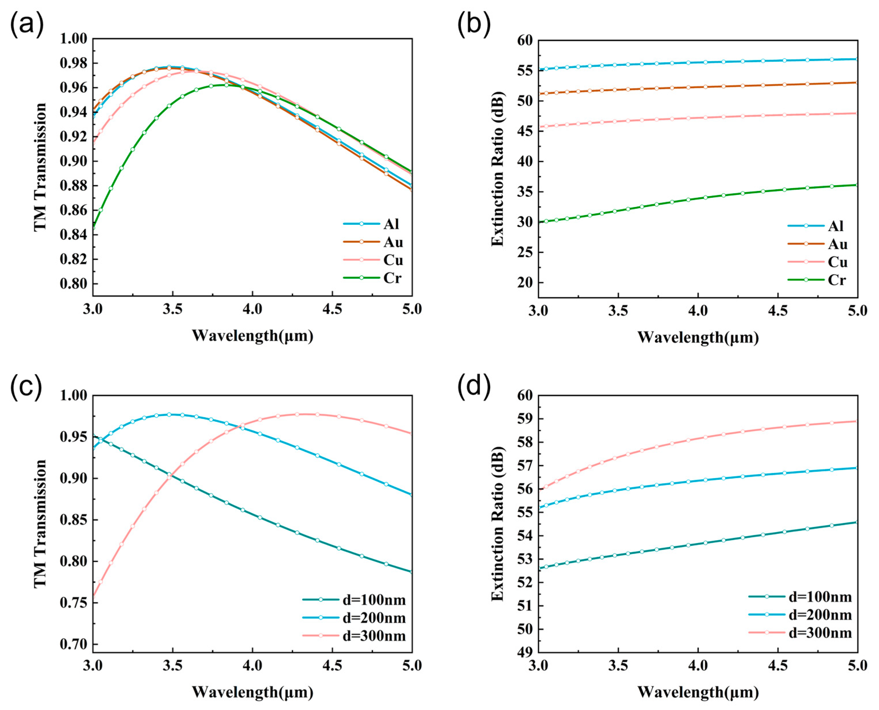
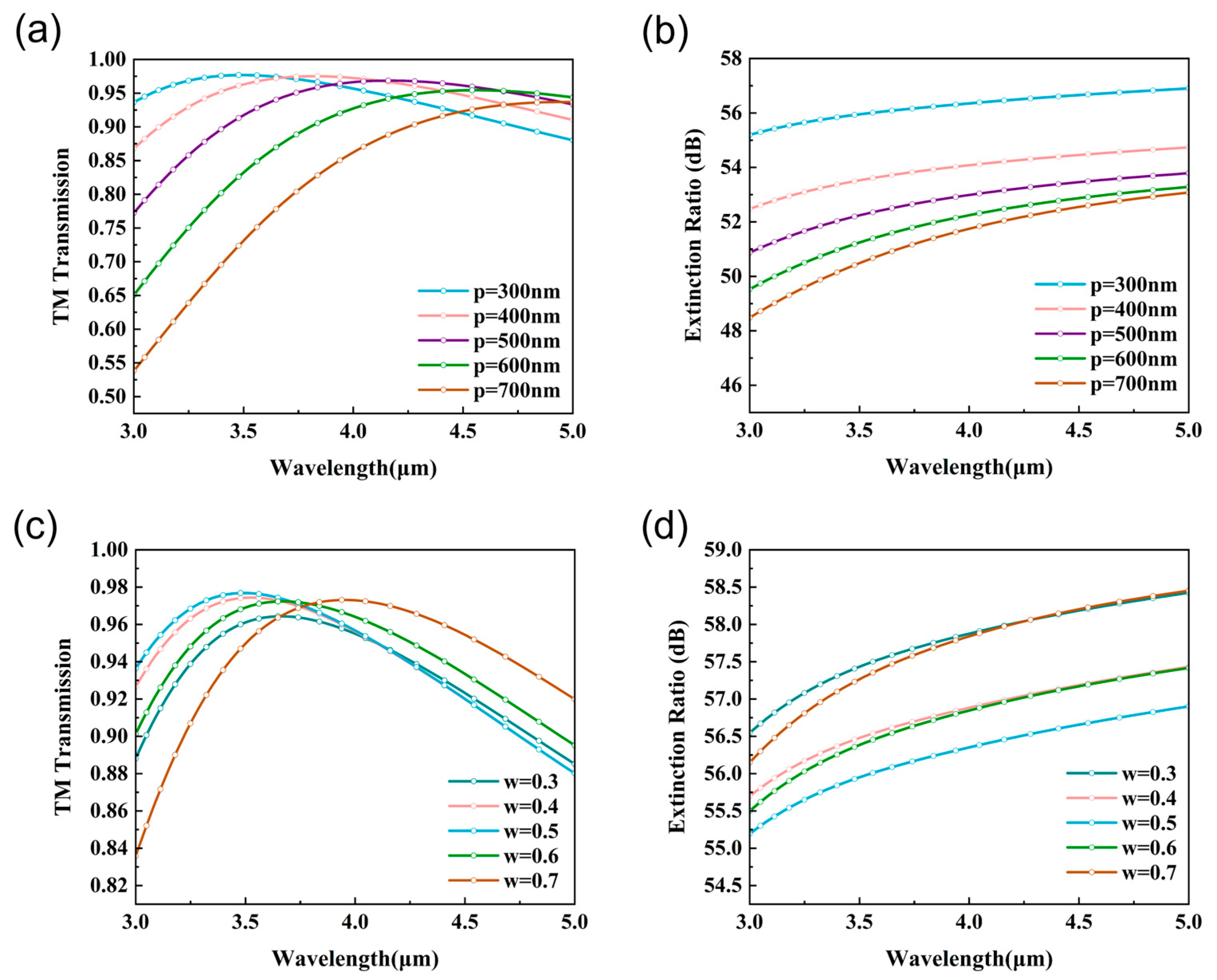
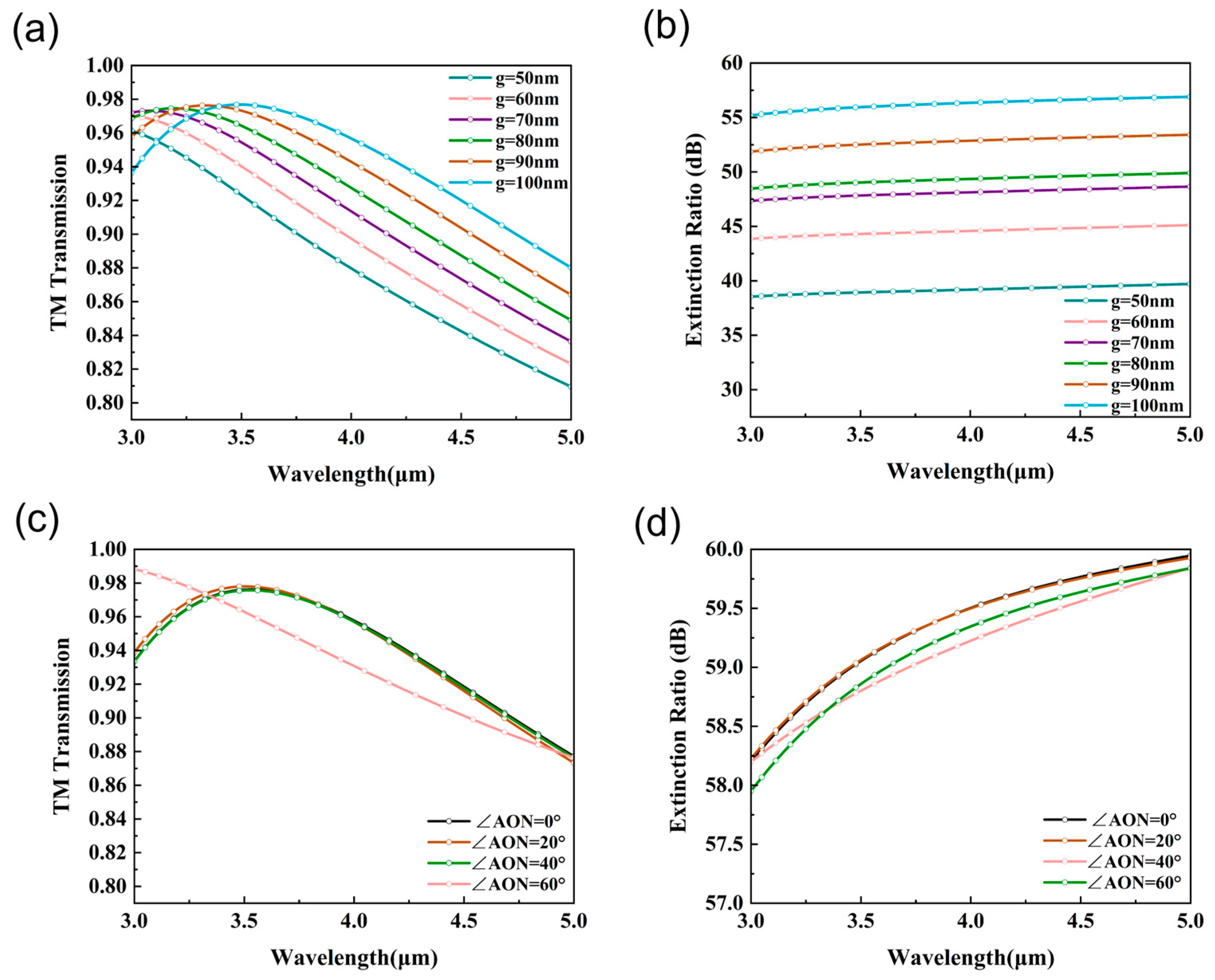
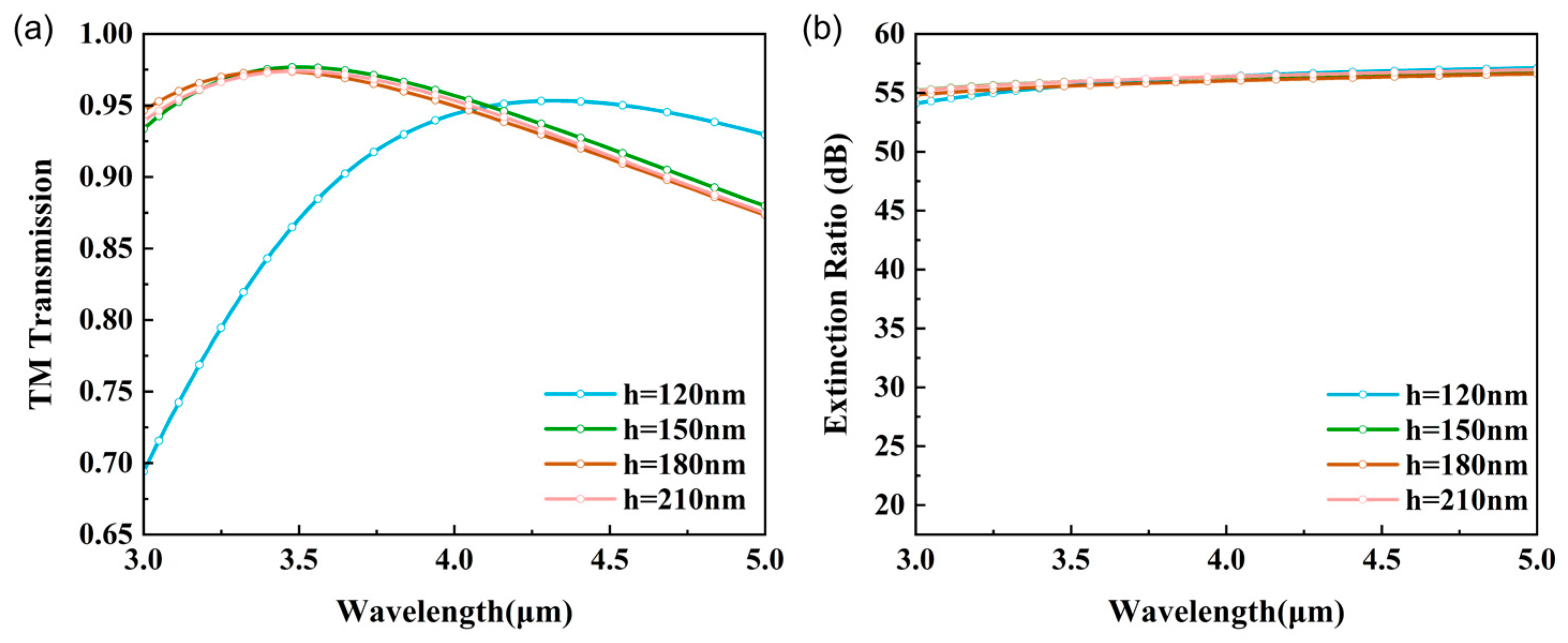
3.1. Structural Optimization

To investigate the effect of structural parameters on polarization performance, the selection of the grating metal-layer material is crucial, as it influences both the polarization characteristics and the fabrication complexity. Figure 2a,b show the effect of four metallic materials, aluminum (Al), gold, copper, and chromium, on the polarization properties. The simulation results showed that using Al as the metal layer resulted in a better extinction ratio compared to the other three materials. This was because Al has a larger imaginary part of the dielectric constant, which enhances the attenuation of TE waves [31], leading to higher extinction ratios. Although aluminum oxidizes in the air, the resulting aluminum oxide does not compromise the grating’s performance. For further details, please refer to Figure S1 in the Supplementary Material. Additionally, Al offers higher overall transmittance in the mid-wave infrared range and is cost-effective to process. Therefore, Al is an ideal choice for the metal layer in the RMBPG structure, and all subsequent simulations used Al as the metal layer.
Figure 2c,d present the optimization of the reflection-reducing film thickness. We started by evaporating a silicon oxide reflective reduction film using conventional coating methods. Due to the high refractive indices of the top grating layer and the bottom InSb absorber layer, and the low refractive index of the intermediate SiO2 waveguide layer, these layers formed a Fabry–Perot (F-P) cavity. The Fabry–Perot (F-P) cavity caused resonance of the light waves entering the cavity, affecting the transmittance of the transmitted waves. To investigate this, we performed simulations with the following parameters: an Al layer thickness of 100 nm, a duty cycle of 0.5, a period of 300 nm, and a variation in the reflection-reducing film thickness in the range of 100 nm to 300 nm. The simulation results showed a significant red shift in the TM wave transmittance peak as the thickness of the reflection-reducing film increased. This can be explained by the F-P resonant cavity theory, where resonance occurs in the cavity when the following conditions are met:
m λ = 2 nL .
As a reflection-reducing film, the optimal thickness of the SiO2 layer varies with the operating wavelength. Considering the spectral range of the mid-wave InSb infrared detector, the SiO2 film thickness was selected to be 200 nm. At this thickness, the TM-wave transmittance in the 3–5 µm range was 88–97%, with extinction ratios reaching 55–57 dB.
In the next step, we optimized the period of the double-layer grating structure. The choice of grating period significantly influenced the transmittance of TM and TE waves, as well as the extinction ratio. Therefore, different grating periods were selected for optimization, ensuring the grating period satisfied p << λ. However, as the grating period decreased, the manufacturing process became more challenging. Consequently, the grating period was chosen to fall within the range of 0.1 μm < p < λmin/3 = 1 μm. The simulated grating periods selected were 0.3 μm, 0.4 μm, 0.5 μm, 0.6 μm, and 0.7 μm. Other parameters needed further optimization, so the initial values were considered preliminary. With the other parameters already optimized, the simulation parameters were set as follows: Al layer thickness of 100 nm, duty cycle of 0.5, and reflective film thickness of 200 nm. The simulation results demonstrated that both the TM-wave transmittance and extinction ratio increased as the period of the double-layer polarization grating decreased, as shown in Figure 3a,b. For periods of 300 nm, the TM-wave transmittance in the mid-wave infrared range reached 88–97%, and the extinction ratio exceeded 55 dB. We found that the RMBPG grating outperformed its counterparts [32]. However, a smaller period increased the difficulty of the manufacturing process. Therefore, a period range of 300–400 nm was chosen for practical fabrication, balancing performance and process feasibility.
We further investigated the impact of the duty cycle of the double-layer polarization grating on polarization performance. For the simulation, we set the double-layer polarization period to 300 nm, the Al layer thickness to 100 nm, and the transmittance-enhancing film thickness to 200 nm. The results differed significantly from those of the traditional single-layer polarization grating, showing a strong dependence on the duty cycle. When the duty cycle was between 0.3 and 0.6, the transmittance in the mid-wave infrared range exceeded 87%, and the extinction ratios were above 55 dB. Additionally, the double-layer polarization grating offered an adjustable duty cycle range, providing flexibility for the subsequent fabrication process.
To further optimize the structural parameters, we also simulated the effect of the metal-layer thickness. Figure 4a,b show how the TM wave transmittance and extinction ratio varied as the Al metal-layer thickness increased from 50 nm to 100 nm. The extinction ratio increased gradually with the metal-layer thickness while the TM wave transmittance decreased near the 3 µm wavelength. Additionally, since the HSQ grating layer thickness was set to 150 nm, an excessively thick metal layer would complicate the fabrication process. Therefore, a metal-layer thickness of 90–100 nm was deemed reasonable for practical fabrication. Normally, the structural properties are different when light is incident from different angles [33]. Figure 4c,d show the effect of different angles of incidence on the transmittance and extinction ratio. There were good results in the range of 0–60 degrees incidence.
Finally, we investigated the influence of the thickness of the HSQ uniform coating on the structural performance. As shown in the Figure 5, the simulation parameters used in the simulation were a period of 300 nm, a metal-layer thickness of 100 nm, a duty cycle of 0.5, and an anti-reflection coating of 200 nm. From the figure, it can be seen that when the thickness of HSQ was 120 nm, the transmittance of the structure was relatively low in the 3–4 μm wavelength range. Therefore, we further increased the thickness of HSQ. When the coating thickness was ≥150 nm, the TM-wave transmittance and the overall extinction ratio of the structure tended to stabilize. However, the aspect ratio will become unstable and increase the difficulty of process preparation as it becomes larger. Therefore, we think that setting the coating thickness between 150 and 210 nm is appropriate.
In summary, when using aluminum as the grating material, a thicker Al layer and a smaller period could lead to a higher extinction ratio. Considering both the transmittance of polarized light and the challenges of fabrication, we have compiled a recommended range of structural parameters for RMBPG, as shown in Table 1: Al as the metal material, a period of 300–400 nm, a duty cycle of 0.3–0.6, a metal-layer thickness of 90–100 nm, an HSQ layer thickness of 150 nm, and a silica reduction film thickness of 200–300 nm. The simulation results showed that the RMBPG structure was an ideal structure for processing and preparation, as the transmittance and extinction ratios were significantly improved compared with those of the same type of grating [34].

3.2. Analysis in Theory

Figure 6a illustrates the polarization phenomenon in the RMBPG structure, explained using the multilayer medium transport matrix model [35,36]. The RMBPG structure can be viewed as a three-layer 1D subwavelength grating: the top layer is an air–Al grating (HAH), the middle layer is an air–HSQ grating (HSQ), and the bottom layer is an Al–HSQ grating (AHA). The equivalent refractive index of each grating layer was calculated using the equivalent medium theory (EMT), an approximation method for hypersurface structures at the physical layer level [37]. The EMT treats the periodic structure of the hypersurface as a homogeneous medium layer for calculation purposes. This approach allows for the design and prediction of hypersurface properties through theoretical calculations. This theory allows us to calculate the equivalent refractive indices nHAH, nHSQ, and nAHA of each grating layer at different wavelengths [38], while, according to the equivalent medium theory, for transverse electrically (TE) polarized light (i.e., the electric-field component is parallel to the grating) and for transverse magnetically (TM) polarized light (i.e., the electric-field component is perpendicular to the grating), the equivalent refractive indices of the grating can be determined as follows [39]:
n TE = f n 1 + i k 1 2 + 1 f n 2 + i k 2 2 ,
n TM = n 1 + i k 1 2 n 2 + i k 2 2 n 2 + i k 2 2 + 1 f n 2 + i k 1 2 ,
where f is the duty cycle of the grating and n1, n2, k1, and k2 are the real and imaginary parts of the refractive index (i.e., extinction coefficients) of the grating material and grating gap material, respectively. The refractive index of the metal grating for TE waves contains only an imaginary component, indicating that most TE-polarized light will be reflected and absorbed. In contrast, for TM waves, the grating’s refractive index has only a real component, allowing most TM-polarized light to transmit. To enhance TM-wave transmittance and TE-wave absorption and reflection, the metal grating material should have a larger imaginary component in its refractive index.
In the multilayer dielectric transmission matrix model, gratings are treated as continuous surfaces that reflect light spectacularly, as the wavelength of incident light is much larger than the grating period. The overall reflection and transmission coefficients of the RMBPG structure depend on the transmission and reflection of each 1D grating layer, which can be obtained through the transmission matrix method [40]. This approach calculates the overall transmission matrix of the RMBPG structure by multiplying the transmission matrices of each layer:
M = M HAH × M HSQ × M AHA ,
where MHAH, MHSQ, and MAHA are the transfer matrices of the top grating, the intermediate grating layer, and the lower grating layer, respectively. The total reflection and transmission coefficients r and t can be derived from the relationship between the total transfer matrix M- and the S-parameters, as follows:
r = r 12 + α r 23 e 2 i β 1 r 21 r 23 e 2 i β ,   t = t 12 t 23 e i β 1 r 21 r 23 e 2 i β ,
where r12 and r21 are the reflection coefficients above and below the HAH grating layer, respectively. r23 is the reflection coefficient from the AHA grating layer; β is the propagation phase factor in the HSQ layer β = k × nHSQ × tHSQ, where nHSQ, k, and tHSQ are the refractive index of the HSQ grating layer, the wave vector in the free space, and the thickness of the HSQ grating layer, respectively; and α is denoted as follows:
α = t 21 t 12 r 21 r 12 ,
where t12 and t21 are the transmission coefficients above and below the upper Al grating, respectively. The full transmission and reflection coefficients could be derived from the r and t coefficients, as follows:
T total = t 2 , R total = r 2 .
The RMBPG structure demonstrated high transmission for TM waves and high reflection for TE waves, as verified by electric-field simulations around the structure (Figure 6b,c). For TM-wave incidence, the electric field was concentrated in the middle and lower regions of the RMBPG, indicating a high transmission mode. For TE waves, the electric field was primarily in the upper region, showing a high reflection mode, which is consistent with our theoretical model. Additionally, the high concentration of the light field within the RMBPG for TM waves significantly enhanced light field efficiency, benefiting the device’s responsivity.

4. Discussion

The optimized RMPBG structure achieved a TM-wave transmittance of 88–97% in the 3~5 um band, with an extinction ratio of 55 dB. Table 2 shows the comparison of the polarization performance of the RMBPG structure with the same type of grating, which outperformed the same type of grating in terms of both broad-spectrum TM-wave transmittance and extinction ratio. This shows that the RMBPG structure provides a viable solution for integrating high performance polarization gratings into IR detectors.
At the same time, the RMBPG structure is easy to integrate on-chip, which is favorable for future applications. As shown in Figure 7, the recommended process steps include: 1. a uniform coating of HSQ on the surface of the detector image element, 2. pattern transfer by electron-beam lithography, and 3. homogenization and deposition of patterned metal layer by electron-beam evaporation (EBE). Compared with the conventional preparation of grating structures, the RMBPG structure has significant advantages: the elimination of the metal stripping or etching step by curing HSQ to act as a dielectric grating layer greatly simplifies the fabrication process and reduces experimental errors. The large area of blind elements in the detector due to the non-uniformity of the adhesive thickness in the fabrication of large-scale gratings is also a major difficulty in the fabrication of conventional focal plane polarization detectors, which is successfully avoided by the RMBPG structure. The structural parameters of the RMBPG grating structure, such as duty cycle, adhesive thickness, and period, can ensure good transmittance and extinction over a wide range. Therefore, the actual structural parameters can still show excellent results when compared with the ideal conditions of simulation, and an HSQ adhesive thickness of more than 150 nm can ensure good results, which can eliminate the process problem of uneven thickness of the adhesive in the production of large-area array detectors, which significantly improves the manufacturability. In the mass production stage, using nanoimprint technology instead of electron-beam lithography can further improve the production efficiency.

5. Conclusions

In conclusion, we present a high-performance polarization grating superstructure that can be fabricated efficiently using cured HSQ e-beam resist. Through FDTD simulations, we investigated the impact of various structural parameters on polarization performance, with theoretical analysis based on the multilayer medium transmission matrix model and the F-P theory. Simulation results demonstrate that the RMBPG structure, with HSQ as the grating layer, achieves excellent polarization performance, high TM-wave transmittance (88–97%), and a high extinction ratio (≥55 dB) across the 3–5 µm spectral range. At the same time, the RMBPG grating outperforms its counterparts. In addition, this structure significantly simplifies fabrication, offering a promising approach for developing large-area focal plane arrays with integrated grating polarizers and advancing polarization detection technology.

Supplementary Materials

The following supporting information can be downloaded at: https://www.mdpi.com/article/10.3390/photonics12030287/s1, Figure S1: Effect of aluminium oxide on grating properties.

Author Contributions

Conceptualization, J.L., J.X., W.W. and H.L.; data curation, J.X. and H.L.; formal analysis, J.L., R.H., G.C., W.W. and P.S.; funding acquisition, Y.W.; investigation, G.C. and H.L.; methodology, J.L., J.X., G.C. and P.S.; project administration, R.H.; resources, Y.W.; software, J.L., J.X. and P.S.; supervision, R.H. and Y.W.; validation, J.X. and W.W.; writing—original draft, J.L. and J.X.; writing—review and editing, R.H. and Y.W. All authors have read and agreed to the published version of the manuscript.

Funding

Aeronautical Science Foundation of China (20240024036001), the open subject of the National Key Laboratory of Infrared Detection Technologies (Grant No. IRDT-23-02 and Grant No. 2024-JJ-103-02), and Yunnan Science and Technology Program Projects (2023032A08001).

Data Availability Statement

Date underlying the results presented in this paper are not publicly available at this time but may be obtained from the authors upon reasonable request.

Conflicts of Interest

The authors declare no conflicts of interest.

References

  1. Gaiarin, S.; Perego, A.M.; da Silva, E.P.; Da Ros, F.; Zibar, D. Dual-polarization nonlinear Fourier transform-based optical communication system. Optica 2018, 5, 263–270. [Google Scholar] [CrossRef]
  2. Dubreuil, M.; Delrot, P.; Leonard, I.; Alfalou, A.; Brosseau, C.; Dogariu, A. Exploring underwater target detection by imaging polarimetry and correlation techniques. Appl. Opt. 2013, 52, 997–1005. [Google Scholar] [CrossRef] [PubMed]
  3. Talmage, D.A.; Curran, P.J. Remote sensing using partially polarized light. Int. J. Remote Sens. 1986, 7, 47–64. [Google Scholar] [CrossRef]
  4. Qi, J.; Tatla, T.; Nissanka-Jayasuriya, E.; Yuan, A.Y.; Stoyanov, D.; Elson, D.S. Surgical polarimetric endoscopy for the detection of laryngeal cancer. Nat. Biomed. Eng. 2023, 7, 971–985. [Google Scholar] [CrossRef]
  5. He, C.; He, H.; Chang, J.; Chen, B.; Ma, H.; Booth, M.J. Polarisation optics for biomedical and clinical applications: A review. Light. Sci. Appl. 2021, 10, 194. [Google Scholar] [CrossRef]
  6. Wu, Y.; Shen, Y.; Addamane, S.; Reno, J.L.; Williams, B.S. Tunable quantum-cascade VECSEL operating at 1.9 THz. Opt. Express 2021, 29, 34695–34706. [Google Scholar] [CrossRef]
  7. Li, L.; Han, W.; Pi, L.; Niu, P.; Han, J.; Wang, C.; Su, B.; Li, H.; Xiong, J.; Bando, Y.; et al. Emerging in-plane anisotropic two-dimensional materials. InfoMat 2019, 1, 54–73. [Google Scholar] [CrossRef]
  8. Wan, M.; Gu, G.; Qian, W.; Ren, K.; Chen, Q. Stokes-vector-based polarimetric imaging system for adaptive target/background contrast enhancement. Appl. Opt. 2016, 55, 5513–5519. [Google Scholar] [CrossRef]
  9. York, T.; Gruev, V. Characterization of a visible spectrum division-of-focal-plane polarimeter. Appl. Opt. 2012, 51, 5392–5400. [Google Scholar] [CrossRef]
  10. Park, H.; Crozier, K.B. Elliptical silicon nanowire photodetectors for polarization-resolved imaging. Opt. Express 2015, 23, 7209–7216. [Google Scholar] [CrossRef]
  11. Bavirisetti, D.P.; Dhuli, R. Two-scale image fusion of visible and infrared images using saliency detection. Infrared Phys. Technol. 2016, 76, 52–64. [Google Scholar] [CrossRef]
  12. Zhou, J.; Guo, L.J. Transition from a spectrum filter to a polarizer in a metallic nano-slit array. Sci. Rep. 2014, 4, 3614. [Google Scholar] [CrossRef] [PubMed]
  13. Yuan, Y.; Fan, F.; Zhao, C.; Kwok, H.-S.; Schadt, M. Low-driving-voltage, polarizer-free, scattering-controllable liquid crystal device based on randomly patterned photo-alignment. Opt. Lett. 2020, 45, 3697–3700. [Google Scholar] [CrossRef] [PubMed]
  14. Shen, Y.; Kim, A.D.; Shahili, M.; Curwen, C.A.; Addamane, S.; Reno, J.L.; Williams, B.S. THz time-domain characterization of amplifying quantum-cascade metasurface. Appl. Phys. Lett. 2021, 119, 181108. [Google Scholar] [CrossRef]
  15. Yamada, I.; Kintaka, K.; Nishii, J.; Akioka, S.; Yamagishi, Y.; Saito, M. Mid-infrared wire-grid polarizer with silicides. Opt. Lett. 2008, 33, 258–260. [Google Scholar] [CrossRef]
  16. Yang, Z.Y.; Zhao, M.; Dai, N.L.; Yang, G.; Long, H.; Li, Y.H.; Lu, P.X. Broadband polarizers using dual-layer metallic nanowire grids. IEEE Photonics Technol. Lett. 2008, 20, 697–699. [Google Scholar] [CrossRef]
  17. Zhang, G.; Cao, B.; Wang, C.; Han, Q.; Peng, C.; Wang, J.; Xu, K.; Yang, H.; Pessa, M. Polarized GaN-based light-emitting diode with an embedded metallic/dielectric subwavelength grating. Thin Solid Film. 2011, 520, 419–423. [Google Scholar] [CrossRef]
  18. Shen, S.; Yuan, Y.; Ruan, Z.; Tan, H. Optimizing the design of an embedded grating polarizer for infrared polarization light field imaging. Results Phys. 2018, 12, 21–31. [Google Scholar] [CrossRef]
  19. Sakamoto, M.; Nhan, H.T.; Noda, K.; Sasaki, T.; Tanaka, M.; Kawatsuki, N.; Ono, H. Polarization-probe polarization-imaging system in near-infrared regime using a polarization grating. Sci. Rep. 2022, 12, 15268. [Google Scholar] [CrossRef]
  20. Xue, Y.; Wang, C.; Zhang, G.; Cao, B. Compound polarized wavelength filters with a single subwavelength structure. Opt. Commun. 2010, 284, 501–509. [Google Scholar] [CrossRef]
  21. Feng, B.; Chen, Y.; Sun, D.; Yang, Z.; Yang, B.; Li, X.; Li, T. Precision integration of grating-based polarizers onto focal plane arrays of near-infrared photovoltaic detectors for enhanced contrast polarimetric imaging. Int. J. Extrem. Manuf. 2021, 3, 035201. [Google Scholar] [CrossRef]
  22. Hobbs, R.G.; Putnam, W.P.; Fallahi, A.; Yang, Y.; Kärtner, F.X.; Berggren, K.K. Mapping Photoemission and Hot-Electron Emission from Plasmonic Nanoantennas. Nano Lett. 2017, 17, 6069–6076. [Google Scholar] [CrossRef] [PubMed]
  23. Chou, S.Y.; Krauss, P.R.; Renstrom, P.J. Imprint of sub-25 nm vias and trenches in polymers. Appl. Phys. Lett. 1995, 67, 3114–3116. [Google Scholar] [CrossRef]
  24. Grigorescu, A.; van der Krogt, M.; Hagen, C.; Kruit, P. 10 nm lines and spaces written in HSQ, using electron beam lithography. Microelectron. Eng. 2007, 84, 822–824. [Google Scholar] [CrossRef]
  25. Choi, S.; Yan, M.; Wang, L.; Adesida, I. Ultra-dense hydrogen silsesquioxane (HSQ) structures on thin silicon nitride membranes. Microelectron. Eng. 2009, 86, 521–523. [Google Scholar] [CrossRef]
  26. Saleem, M.R.; Stenberg, P.A.; Khan, M.B.; Khan, Z.M.; Honkanen, S.; Turunen, J. Hydrogen silsesquioxane resist stamp for replication of nanophotonic components in polymers. J. Micro/Nanolithography MEMS MOEMS 2012, 11, 013007. [Google Scholar] [CrossRef]
  27. Makita, M.; Karvinen, P.; Guzenko, V.A.; Kujala, N.; Vagovic, P.; David, C. Fabrication of diamond diffraction gratings for experiments with intense hard x-rays. Microelectron. Eng. 2017, 176, 75–78. [Google Scholar] [CrossRef]
  28. Zeng, P.; Feng, Z.; Zheng, M.; Gao, X.; Zhang, S.; Wang, Y.; Chen, Y.; Duan, H. Dimension and process effects on the mechanical stability of ultra-small HSQ nanopillars. J. Nanoparticle Res. 2021, 23, 255. [Google Scholar] [CrossRef]
  29. Chen, H.-T.; Zhou, J.; O’hara, J.F.; Chen, F.; Azad, A.K.; Taylor, A.J. Antireflection Coating Using Metamaterials and Identification of Its Mechanism. Phys. Rev. Lett. 2010, 105, 073901. [Google Scholar] [CrossRef]
  30. Cao, G.; Xu, H.-X.; Zhou, L.-M.; Deng, Y.; Zeng, Y.; Dong, S.; Zhang, Q.; Li, Y.; Yang, H.; Song, Q.; et al. Infrared metasurface-enabled compact polarization nanodevices. Mater. Today 2021, 50, 499–515. [Google Scholar] [CrossRef]
  31. Ebbesen, T.W.; Lezec, H.J.; Ghaemi, H.F.; Thio, T.; Wolff, P.A. Extraordinary optical transmission through sub-wavelength hole arrays. Nature 1998, 391, 667–669. [Google Scholar] [CrossRef]
  32. Lee, J.-K.; Kim, B.O.; Park, J.; Kim, J.B.; Kang, I.-S.; Sim, G.; Park, J.H.; Jang, H.-I. A bilayer Al nanowire-grid polarizer integrated with an IR-cut filter. Opt. Mater. 2019, 98, 109409. [Google Scholar] [CrossRef]
  33. Qian, L.; Zhang, D.; Huang, Y.; Tao, C.; Hong, R.; Zhuang, S. Performance of a double-layer guided mode resonance filter with non-subwavelength grating period at oblique incidence. Opt. Laser Technol. 2015, 72, 42–47. [Google Scholar] [CrossRef]
  34. Deng, S.-R.; Lu, B.-R.; Dong, B.-Q.; Wan, J.; Shu, Z.; Xue, J.; Chen, Y.; Huq, E.; Liu, R.; Qu, X.-P. Effective polarization control of metallic planar chiral metamaterials with complementary rosette pattern fabricated by nanoimprint lithography. Microelectron. Eng. 2010, 87, 985–988. [Google Scholar] [CrossRef]
  35. Astilean, S.; Lalanne, P.; Palamaru, M. Light transmission through metallic channels much smaller than the wavelength. Opt. Commun. 2000, 175, 265–273. [Google Scholar] [CrossRef]
  36. Liu, J.; Wang, W.; Xie, F.; Zhang, X.; Zhou, X.; Yuan, Y.; Wang, L. Excitation of surface plasmon polariton modes with double-layer gratings of graphene. Nanomaterials 2022, 12, 1144. [Google Scholar] [CrossRef]
  37. Yang, Z.; Feng, B.; Lu, B.; Chen, Y.; Li, W.; Zhang, W.; Li, T. A study of nano-structural effect on the polarization characteristics of metallic sub-wavelength grating polarizers in visible wavelengths. Microelectron. Eng. 2020, 227, 111327. [Google Scholar] [CrossRef]
  38. Jing, X.; Jin, Y. Transmittance analysis of diffraction phase grating. Appl. Opt. 2010, 50, C11–C18. [Google Scholar] [CrossRef]
  39. Zhiwen, W.; Wei, Y.; Jinliang, G. Polarization transmission mechanism analyzation of bi-layer nanowire polarizer. Opt. Commun. 2018, 424, 127–130. [Google Scholar] [CrossRef]
  40. Sun, J.; Liu, L.; Dong, G.; Zhou, J. An extremely broad band metamaterial absorber based on destructive interference. Opt. Express 2011, 19, 21155–21162. [Google Scholar] [CrossRef]
  41. Li, H.; Hao, R.; Chen, G.; Wang, W.; Sheng, P.; Xu, J.; Liu, J.; Li, Y.; Kong, J.; Zhao, J. Optimization of the inverted “T”-shaped double-layer subwavelength grating design integrated on an InSb detector. Opt. Commun. 2024, 573, 131016. [Google Scholar] [CrossRef]
  42. Kong, Y.; Liu, D.; Luo, H. Effect of magnetic polaritons on the polarization characteristics of metal–dielectric–metal infrared wire-grid polarizers. Opt. Commun. 2020, 474, 126111. [Google Scholar] [CrossRef]
Figure 1. (a) Schematic structure of infrared focal plane detector on-chip integrated RMBPG. (b) FDTD simulation model.
Photonics 12 00287 g001
Figure 2. The influence of metal-layer material and thickness of reflection-reducing film on the polarization performance of RMBPG structure. (a,c) TM-wave transmittance. (b,d) Extinction ratio.
Photonics 12 00287 g002
Figure 3. Effect of period and duty cycle on the polarization performance of RMBPG structure. (a,c) TM-wave transmittance. (b,d) Extinction ratio.
Photonics 12 00287 g003
Figure 4. Effect of metal-layer thickness and angle of incidence on the polarization properties of RMBPG structures. (a,c) TM-wave transmittance. (b,d) Extinction ratio.
Photonics 12 00287 g004
Figure 5. Effect of HSQ film thickness on the polarization properties of RMBPG structures. (a) TM-wave transmittance. (b) Extinction ratio.
Photonics 12 00287 g005
Figure 6. (a) Transmission and reflection mechanism of the RMBPG structure. (b) Structural electric-field distribution at TM-wave incidence. (c) Structural electric-field distribution at TE-wave incidence.
Photonics 12 00287 g006
Figure 7. Preparation flow of the detector for on-chip integrated RMBPG structure.
Photonics 12 00287 g007
Table 1. Optimization results of polarization grating parameters.
ElementMaterialPitch/nmDuty CycleMaterial Thickness/nmSiO2 Layer Thickness/nm
ResultsAl300–4000.3–0.690–100200–300
Table 2. Comparison of polarization properties of different subwavelength structures.
Structure TypeMethodsTM
Transmission (%)
Extinction
Ratio (dB)
Reference
Broadband polarizerSimulation38–9447–70[16]
An embedded grating polarizerSimulation84>27.9[18]
Inverted ‘T’-shaped double-layer gratingSimulation>75>53[41]
Metal–electrolyte–metal wire gridsSimulation<89<42[42]
Readily manufactured bilayer polarization gratingSimulation88–97>55This work
Disclaimer/Publisher’s Note: The statements, opinions and data contained in all publications are solely those of the individual author(s) and contributor(s) and not of MDPI and/or the editor(s). MDPI and/or the editor(s) disclaim responsibility for any injury to people or property resulting from any ideas, methods, instructions or products referred to in the content.

