1. Introduction
Over the past seven decades, substantial efforts have been made to develop optical computers for real-time data processing owing to their potential advantages in terms of speed and parallelism over electronic computers [
1,
2,
3]. Notwithstanding these efforts, optical computing has failed to outpace digital computing, which has advanced more rapidly and offers greater power, ease of use, and flexibility [
4]. Optical computing remains predominantly analog, while electronic computing is digital. This fundamental difference has posed challenges, as digital optics lack the necessary components to compete directly with electronics. By contrast, free-space optics [
3] and smart pixels [
5,
6] represent promising solutions for overcoming the limitations of electronic processors, particularly in artificial neural networks [
7]. Purely electrical neural networks face a complex topology of connections as the number of input and output nodes increases, which can cause significant electromagnetic crosstalk or noise, specifically at high clock rates [
3,
4]. However, light paths in free-space optics can cross without electromagnetic crosstalk, simplifying interconnections and reducing fabrication costs. This feature is particularly advantageous in neural networks, which are inherently analog and tolerant to some input errors [
7]. Consequently, researchers have proposed a hybrid approach, combining optics and electronics, leveraging optics for tasks where it excels [
1].
Extensive research has been conducted on optical neural networks (ONNs); however, their complexity and bulkiness have hampered their commercial success compared to digital electronics [
1,
2,
8,
9,
10,
11,
12,
13,
14,
15,
16]. Some ONNs based on photonic integrated circuits [
9,
10] have been successful. However, they use physical waveguides that cannot cross each other, resulting in lower space efficiency and reduced parallel throughput for a given connection density. To simplify the system and reduce optical crosstalk while maintaining immense optical parallelism from free-space optics, ONNs based on Köhler illumination using lens arrays and a spatial light modulator have been suggested, and their performances have been analyzed [
17,
18,
19]. In these types of systems, optics have been used for linear calculations, while smart pixels or electronics have been employed for nonlinear calculations. Furthermore, this architecture has evolved into a bidirectional ONN (BONN) [
19] to handle backward data flow, such as the backpropagation algorithm. The capability of sending data in the backward direction also enables a two-mirror-like BONN (TMLBONN) [
19], which emulates multilayer calculations, saving considerable hardware space. However, for the successful implementation of the backpropagation algorithm in a BONN, it is essential to develop a fast spatial light modulator (SLM) capable of handling frequent changes in data flow. The change in data flow demands the updating of weights in each layer at a fast rate, exceeding several hundred megahertz. Nevertheless, most currently available SLMs are slow and only serially addressable, resulting in considerable latency [
20,
21]. Despite recent advancements in microelectromechanical systems (MEMSs) technology, most SLMs still operate in the range of tens of kilohertz, which is significantly slower than electronic switches. Therefore, the slow speed of currently available SLMs causes considerable latency within the BONN architecture.
To address these challenges, we propose an optical neural network (ONN) based on free-space optics that incorporates lens arrays and a smart pixel light modulator (SPLM). The ONNs presented here are advancements of previously reported architectures, such as the linear combination optical engine (LCOE) [
17] and BONN [
19]. By replacing the SLM in earlier systems with the SPLM, we achieve significantly higher modulation speeds, resulting in a faster refresh rate for weights in the ONN. This enhanced refresh rate makes BONN and TMLBONN more practical for real-world applications. BONN enables backward data flow, which is critical for learning algorithms, while TMLBONN saves significantly more hardware resources by emulating a multi-layer neural network. Thus, integrating SPLM into ONN technology may pave the way for developing more versatile and practical ONNs using current smart pixel technologies.
Additionally, we analyze the performance of the SPLM-based ONN (SPONN) and explore how memory usage in the SPLM influences the scalability of the ONN. Unlike previous systems, this approach eliminates the need for clustering techniques to increase the number of input and output nodes, offering a more streamlined and efficient solution.
2. Materials and Methods
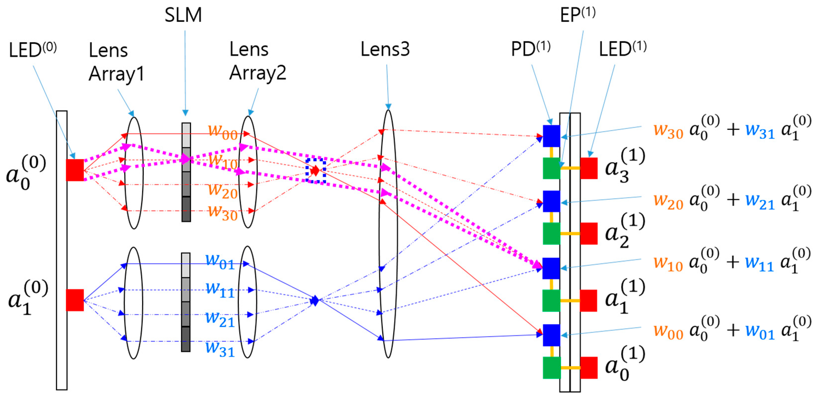
In an ONN based on free-space optics [
17], an SLM is used to represent the weights of the neural network, as shown in
Figure 1. Lens 1 distributes the input light into the pixels of the SLM, and Lens2 focuses the rays from the pixels, making the ray slopes different according to the relative position of the pixel from the optical axis of Lens1 and Lens2. Lens3 forms the images of the pixels on the detector plane, collecting rays of equal inclination into the same spot. This Köhler illumination scheme realizes the neural network connection with minimal optical crosstalk between the channels.
Rays from the input nodes pass through Lens1, the SLM, Lens2, and Lens3 until they reach the photodiode (PD). This optical process performs the linear calculations of the neural network in a single step, increasing throughput considerably. If the numbers of input and output nodes constitute two-dimensional N × N and M × M arrays, respectively, then the total number of interconnections is N
2 × M
2. The rest of the neural network involves the application of a nonlinear function and sending the result to the next stage, which can be efficiently handled by an electronic processor (EP) as in smart pixels. Because the smart pixels on the detector plane are connected only locally with neighboring pixels, the parallelism of the system is not compromised. Although optical nonlinearities enable faster computing without electronic delays [
14], they are difficult to control and reconfigure precisely in large arrays with small form factors. In this paper, this role is performed by the EP or smart pixel. This reflects the direction of LCOE in designing ONNs to be general-purpose and programmable.
This LCOE architecture shows immense optical parallelism with fixed weights in the neural network, which can be very useful, particularly in inference applications. Although the SLMs are reconfigurable and programmable, the switching speed of currently available SLMs remains at a few kilohertz [
20,
21], which delays calculations and significantly reduces throughput if the weights need to be changed during calculations.
There are two potential solutions for improving the refresh rate of the SLM. The first is to develop a fast SLM array, such as absorption modulators. However, this approach involves significant time, effort, and cost. The second solution is to utilize existing technologies, such as smart pixels, which can integrate the detector, light source, and EP into a chip form. Recently, optoelectronic packaging technologies have advanced significantly, making the hybridization of these devices into an array feasible [
6]. Additionally, the EP can perform various functions with memory, making the ONN more programmable and intelligent compared to using SLMs alone.
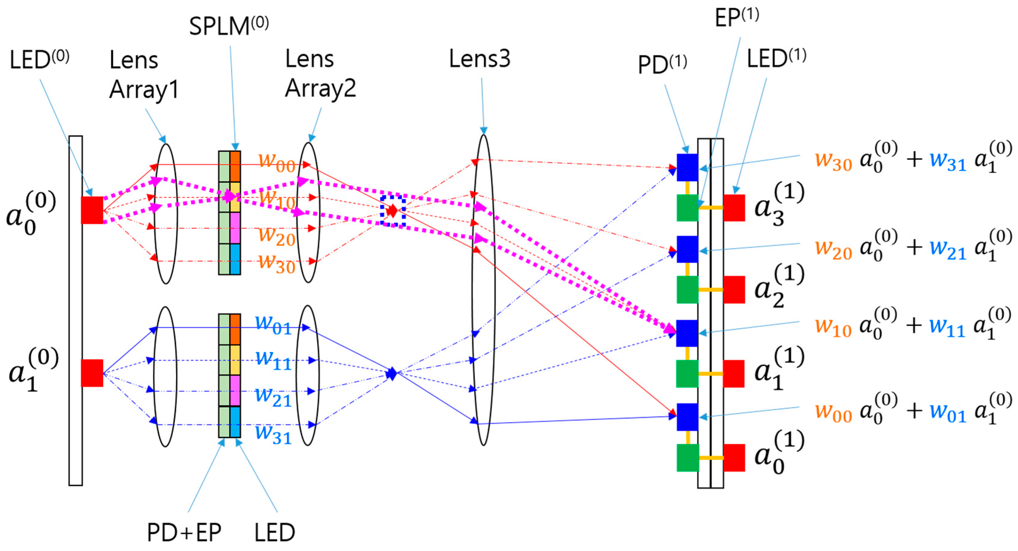
A simple form of the ONN using SPLM is shown in
Figure 2. The SPLM replaces the SLM in the previous LCOE system, while the other parts remain unchanged. The SPLM comprises a PD, an EP, and a light-emitting diode (LED) [
6]. Since LEDs have some limitations in modulation speed, they can be replaced with multi-mode vertical-cavity surface-emitting lasers for higher modulation speeds [
19,
22,
23]. The PD receives the incoming light, converts it into an electrical signal, and sends it to the EP inside the SPLM. The EP amplifies the electrical signal as per the weight value stored in its inherent memory. The output from the EP is sent to the LED, which emits light proportional to the input and weight. The PD, EP, and LED form a pixel, and such pixels are only locally connected except when the program is being downloaded. Once the program is loaded, the array of pixels operates independently, maintaining the parallelism of the system. Each pixel essentially functions as a small repeater.
Because the components are electronic, the modulation speed exceeds several hundred megahertz, which is much higher than that of typical SLMs such as liquid crystal displays (LCDs) and MEMS [
20,
21]. Although the use of SPLM introduces two additional steps of conversion between optical and electronic signals, the delay from this process is less than a few nanoseconds [
6]. However, the gain from the high modulation speed of the SPLM is much greater in many applications, as mentioned in the introduction.
Another difference between the SPONN and the SLM-based ONN is that the LED output of the SPLM changes the divergence of the rays, whereas the SLM maintains collimated light. This issue can be mitigated by using a small lens after the LED. However, this diverging beam does not affect the performance of the ONN because the SLM or SPLM plane is conjugate to the detector plane of the ONN through Lens2 and Lens3. This means the image of the LED in the SPLM forms at the detector plane regardless of the divergence angle of the LED.
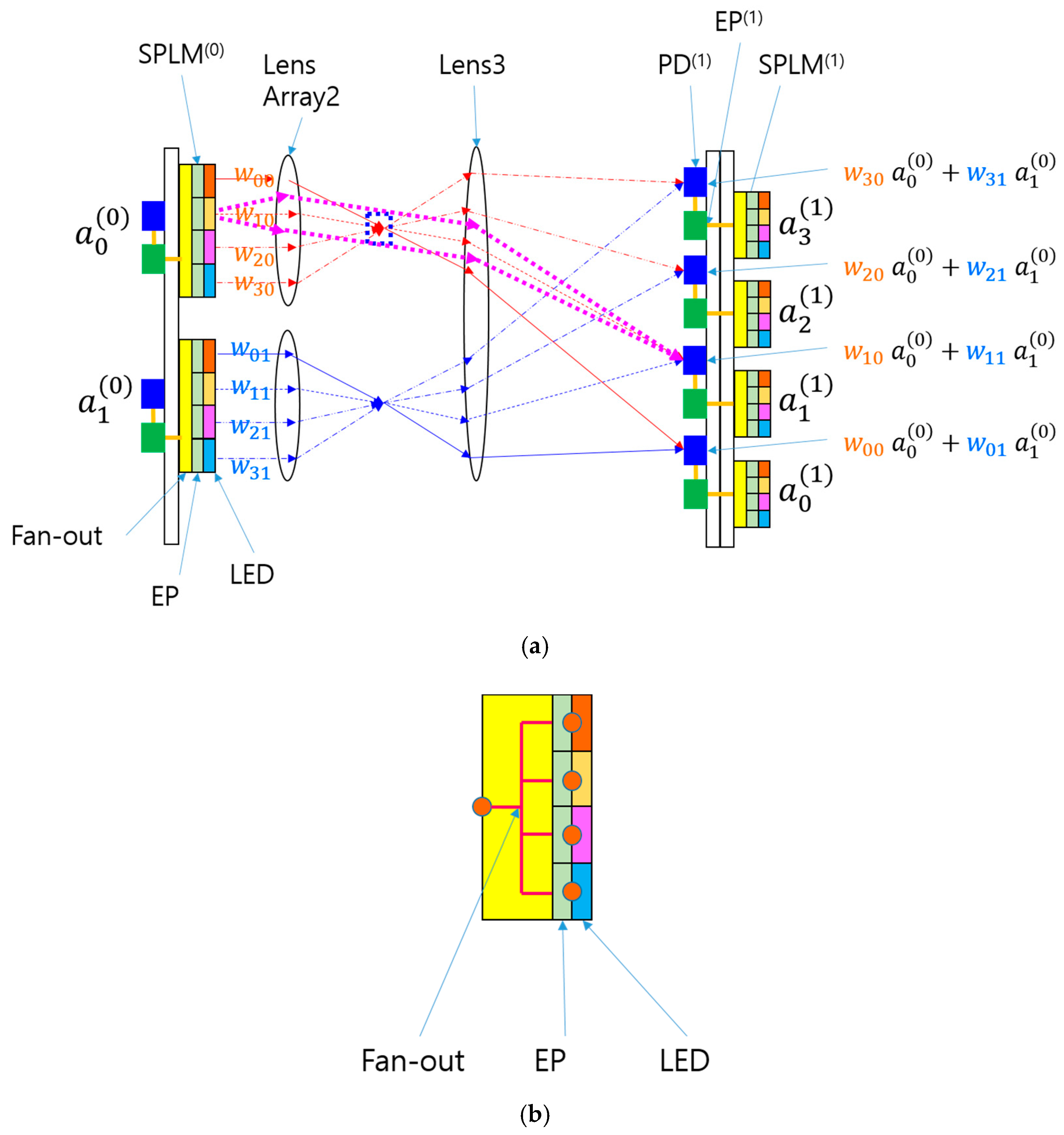
The SPONN can be further simplified by replacing LED
(0) and Lens1 with an electrical fan-out, as shown in
Figure 3a. The electrical fan-out is illustrated in detail in
Figure 3b. The light input and Lens1 function as an optical distributor of the input signal, while the electrical fan-out in
Figure 3a,b serves as an electrical distributor. This electrical distributor has a simple wiring topology that connects the output of the preceding layer to the inputs of the pixels in the following SPLM. This simple topology reduces wiring complexity and electromagnetic noise. By using an electrical fan-out, the number of components and the burden of optical alignment can be reduced, thereby simplifying the system.
The removal of LED
(0) and Lens1 simplifies the optics and eliminates the need for Köhler illumination, in which Lens1 and Lens2 form a condenser system and Lens2 and Lens3 form a projection system. With only the projection system remaining, further simplification is possible, as shown in
Figure 3c. In this configuration, the distance between Lens2 and Lens3 can be shortened, or they can be combined into a single lens using cementing or a diffractive optical element (DOE). Combining them into one element saves space and reduces the burden of optical alignment, leading to cost reduction. Each layer of the system comprises an input smart pixel array, a lens array, and an output detector array with a smart pixel array.
Overall, the replacement of SLM by SPLM greatly simplifies the system and may reduce fabrication difficulty and cost in the future. A three-dimensional view of the SPONN is shown in
Figure 3d. This architecture is cascadable and accommodates multilayer ONNs like the LCOE.
3. Results
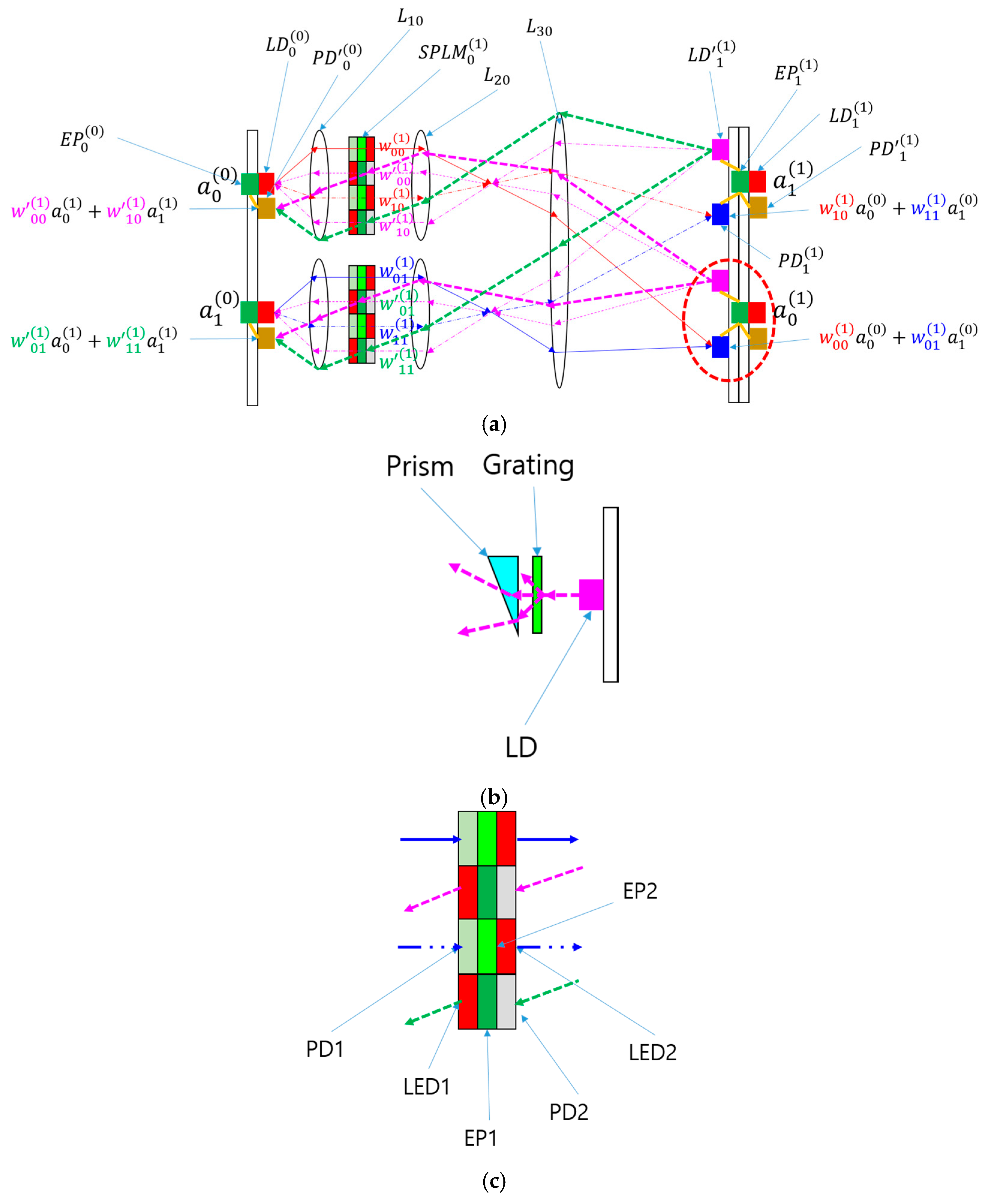
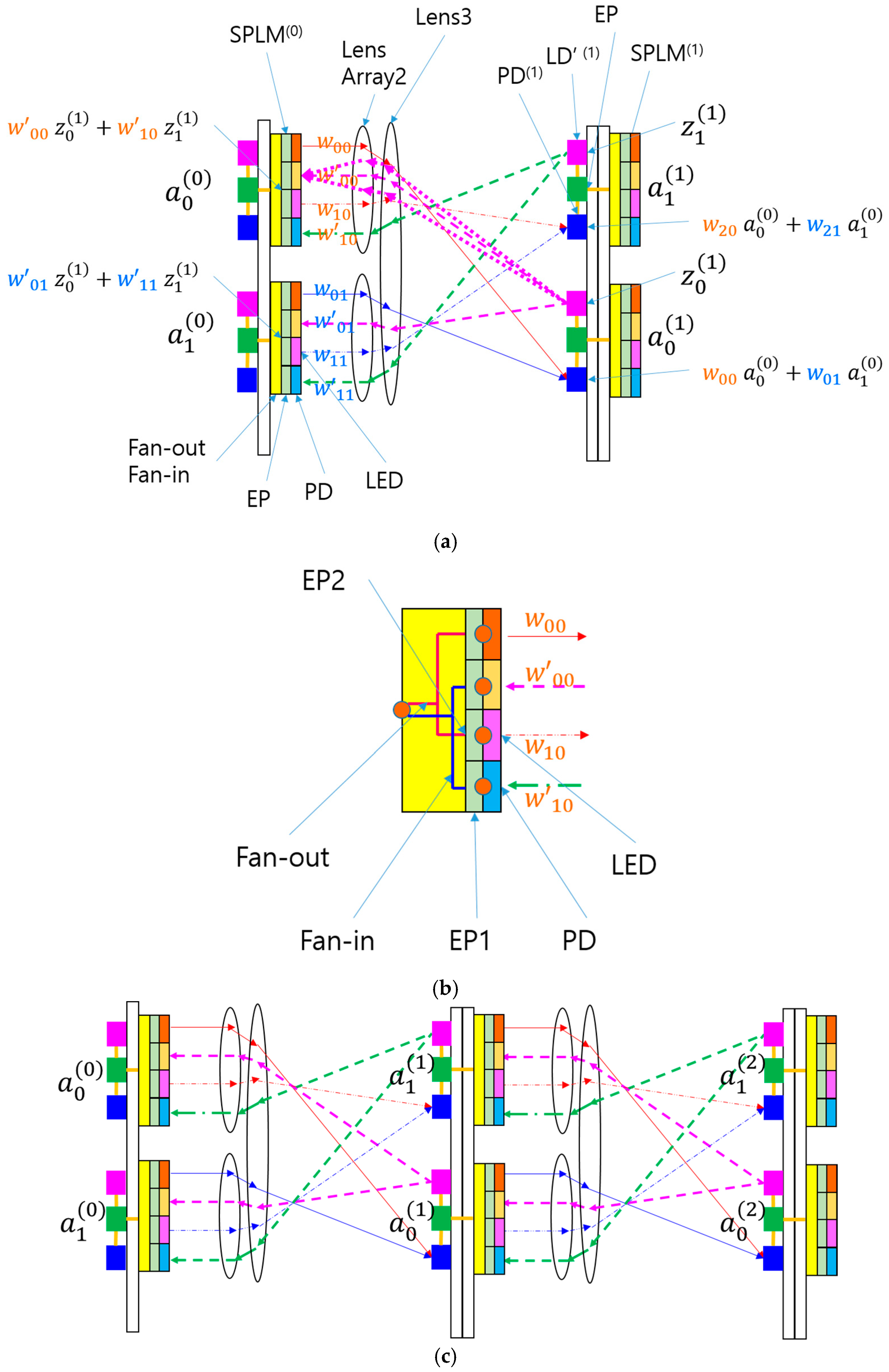
The application of SPLM in an ONN can also be extended to BONN [
19], as illustrated in
Figure 4a. In the SPLM-based BONN (SPBONN) architecture, the SPLM replaces the SLM, which was previously responsible for modulating light propagating in both forward and backward directions according to the weight values of the neural network [
19]. The images of the SPLM pixels are formed on the detectors in the second substrate or the detector plane using Lens2 (
L20) and Lens3 (
L30). The second substrate also includes light sources (
) for backward propagation, as shown in
Figure 4b. The light source for the backward direction can include a laser diode, grating, and prism to control the properties of the output beams, which pass through the SPLM and focus on the PDs (
) on the first substrate for the backward direction. This entire BONN scheme is preserved even after replacing the SLM with SPLM, with the key improvement being a dramatic increase in modulation speed.
Because the SPLM can modulate light at several hundred megahertz, the refresh rate of the weights of the neural network can also reach a few hundred megahertz, as the next weight stored in the EP memory is sent to the amplifier within a few nanoseconds. This high refresh rate eliminates most of the concerns associated with the slow modulation of SLM in the previous BONN architecture. Replacing the SLM with SPLM enables the practical implementation of the backpropagation algorithm and the TMLBONN structure without the need for developing new types of fast SLM array devices. The implementation details of the backpropagation algorithm in BONN, along with the benefits of TMLBONN within the BONN architecture, are discussed in reference [
19].
The SPLM used in this BONN differs from those in
Figure 2 and
Figure 3; the details are shown in
Figure 4c. To enable bidirectional modulation, the pixels are divided into two groups. One group is dedicated to the forward direction, featuring PD1 on the left side and LED2 on the right side of the same pixel, connected via EP2. The other group is designed for the backward direction, with PD2, EP1, and LED1 within a pixel to modulate light in reverse. LED1 may include a microprism or lens to control emission and divergence angles.
As with the simplification from
Figure 2 to
Figure 3, a similar approach can be applied to transform the SPBONN in
Figure 4 into that in
Figure 5 by using electrical fan-in and electrical fan-out to replace the optical input distribution previously achieved with Lens1. The final SPBONN design comprises SPLM, lenses, and detectors on the second substrate, maintaining the same bidirectional data flow while significantly simplifying the hardware structure. The electrical fan-in is introduced to perform the analog summing of optical signals for the backward direction, as in the previous version of the BONN. The EPs within the SPLM convert the output into current, and the electrical fan-in aggregates this current into the electrical input/output node of the EPs in the preceding layer. An example of a multilayer SPBONN is displayed in
Figure 5c, which uses the cascading feature of SPBONN. The number of layers can be expanded further to increase parallel throughput for continuous input data.
To assess the SPBONN, it is important to understand the scalability of the BONN system, which is inherited from the LCOE [
17,
19]. The core of the SPBONN lies in its projection system, comprising Lens2 and Lens3, as shown in
Figure 5. This system faces scalability limitations if clustering techniques are not employed [
17,
19]. Geometrical aberrations and image magnification restrict the size of the input and output arrays to less than 192 × 192 if the worst-case angular aberration is 1 mrad and the f-number (f/#) of Lens2 is 2, respectively. Each bidirectional channel requires four subchannels to manage forward and backward data flow in the difference mode. Consequently, the maximum input or output array size is limited to 96 × 96 under the optical constraints outlined in reference [
17]. This array size enables approximately (96 × 96)
2, or 8.5 × 10
7, parallel multiply-and-accumulate (MAC) operations per instruction cycle. Assuming a delay of approximately 10 ns in the SPLM and an additional 10 ns delay in the detector plane of the second substrate [
6], the parallel throughput of a single layer is estimated to be 4.3 × 10
15 MAC/s. This throughput can be further increased as the number of layers increases, provided the data flow remains continuous, as in inference applications, similar to pipelining in a digital computer, with multiple layers operating simultaneously. For example, if there are 10 layers, the throughput could reach 4.3 × 10
16 MAC/s, surpassing the throughput of a tensor processing unit by nearly 100 times [
24].
The above estimation does not apply to the backpropagation algorithm, as the data flow during backpropagation occurs in a single pass after the forward calculation. In this scenario, calculations are performed one layer at a time, which means that multiple layers are not activated simultaneously, thereby offering no gain from using multiple layers. In the LCOE architecture, multiple layers are necessary for maintaining high optical parallelism because the refresh rate of weights or the SLM is only a few kilohertz. However, SPBONN does not require multiple layers, which would not only demand significant hardware space, but also involve substantial fabrication and assembly efforts, leading to high costs. The SPLM-based TMLBONN architecture addresses this issue by effectively handling the multilayer sequential algorithm, thereby saving hardware resources. The data flow bouncing between two layers can emulate a multilayer ONN because the weight refresh takes only 10 ns, which can occur during the calculation on the detector plane in the preceding layer. Consequently, there is no additional delay due to weight updates for the next layer.
4. Discussion
The energy consumption of SPBONN needs to be evaluated, as SPLMs may consume more power than SLMs. SLMs, such as LCDs, are highly energy efficient devices that only rotate liquid crystals using an electric field without generating significant heat. However, SPLMs contain light sources such as LEDs or LDs, which emit light and can generate heat, particularly in large arrays. For example, if each SPLM output pixel in
Figure 5b uses a micro-LED measuring 5 × 5 µm
2 and consuming approximately 1 µW—with a typical current density of 1 A/cm
2 [
25] and an optical output power of around 0.25 µW—a 96 × 96 input and output array would require 2 × (96 × 96)
2 LEDs in the SPLM array. The total electrical power consumption would be approximately 170 W. This amount of heat could be dissipated via natural or forced convection without significantly increasing the device’s temperature, provided the board or substrate, including the light sources, is not excessively small. If the SPLM pixels are spaced 20 μm apart, the total size of the SPLM array would be 370 × 370 mm
2, which may be large enough for effective heat dissipation using convection alone. Considering that the throughput of a single-layer SPBONN decreases to the level of a tensor processing unit [
24], the power consumption drops to only 17 W, which is very low compared to that of an electronic neural network.
Replacing the SLM with the SPLM enhances the functionality of the ONN, as each smart pixel contains an EP that is programmable and has memory for storing weight data. This memory can be used to scale the number of input and output nodes with some time delay. Previously, the scaling limits of ONNs were overcome by using clustering techniques in hardware, where multiple ONN modules were stacked in layers to redistribute extended input data and make full connections between the doubled input and output nodes [
17]. However, SPONN eliminates the need for hardware scaling by using memory to increase the number of input and output nodes.
The process of doubling the input and output nodes is illustrated in
Figure 6. First, a full connection is made between the first group of N input nodes and the first group of N output nodes, with the output nodes storing the first output group in memory, as shown in
Figure 6a. Next, the first input group is connected to the second group of N output nodes, and the first input group is stored in memory while the second input group is loaded into the input nodes using the memory of the input smart pixels, as shown in
Figure 6b. Then, the second input group is fully connected with the second output group, as depicted in
Figure 6c. Because the second output group accumulates all the weighted outputs from both the first and second input groups, it is stored in memory and replaced by the first output group, as shown in
Figure 6c. Finally, the second input group is fully connected to the first output group to complete the first output group, as shown in
Figure 6d, which now contains the weighted outputs from both the first and second input groups. The process of doubling the input and output nodes is summarized in the form of a logic diagram, as shown in
Figure 6e.
This method of doubling input and output nodes can be repeated to further increase the number of nodes. The entire doubling process requires nine steps, which introduces some calculation delays and reduces throughput; however, it provides a way to expand the number of input and output nodes without additional hardware scaling. This approach saves on cost and space, offering flexibility for ONNs to accommodate various input and output sizes.
Smart pixel memory in SPONN can also be used to perform ONN operations in difference mode. In the LCOE configuration, handling negative weights requires an additional optical channel to obtain the weighted outputs and subtract them from the outputs of positive weights. However, in SPONN, inputs are first connected to the positive weights, and the weighted outputs are stored in the smart pixel memory on the second substrate. The positive weights are then replaced with negative weights, and the outputs are recalculated. The negative weighted outputs are subtracted from the positive ones stored in memory. Although this process introduces a slight delay due to the additional steps, it requires only half as many output nodes as the traditional difference mode. Thus, SPBONN can emulate the difference mode using smart pixel memory, with a minimal delay when sufficient input and output nodes are unavailable. This approach is practical because the fast weight refresh rate of the SPLM significantly reduces the impact of the delay.
If typical SLMs are used instead of SPLMs to handle positive and negative weights separately by refreshing weight values, the delay increases to at least 10 μs, compared to just 10 ns for SPLMs. This excludes the time required for serialization and loading input data into the SLM array. Consequently, replacing SLMs with SPLMs results in a throughput improvement of over 10,000 times. A similar advantage is observed in applications where the same input data is applied to different sets of weight values. The throughput gain becomes particularly evident with SPLMs in ONN systems, as they significantly reduce the delay when switching between different weight sets.
Furthermore, scaling input and output nodes falls under the multiple weight set scenario. Doubling the input and output nodes causes the number of interconnections to increase fourfold, while the number of calculation steps rises ninefold. If a calculation step using SPLMs takes 10 ns [
6], then doubling the scale requires 90 ns, whereas the same calculation using SLMs takes 900 μs. Consequently, the parallel throughput of a single layer, as described at the end of the previous section, is estimated to decrease to approximately 1.9 × 10
15 MAC/s and 1.9 × 10
11 MAC/s for SPLMs and SLMs, respectively. Therefore, SPBONN does not significantly degrade parallel throughput while doubling the input and output nodes, thereby providing greater flexibility for ONN.
Compared to previous ONNs [
15,
16,
17,
19], the SPONN architecture offers significant advantages in terms of flexibility and reconfigurability. Earlier ONNs, such as hologram-based ONNs [
11] and diffractive deep neural networks [
15,
16], relied on DOEs to represent both the linear and non-linear components of a neural network. While these diffractive optics provided a fast, fully optical implementation, they were neither reconfigurable nor programmable, limiting their applications. Furthermore, hologram-based ONNs [
11] lack cascading capability, which critically hinders the implementation of multilayer neural networks. Other ONNs, such as LCOE [
17] and BONN [
19], used SLMs, making them reconfigurable, but the slow speed of current SLMs hinders real-time weight updates. To maintain optical parallelism with slow SLMs, multiple layers need to be applied in a cascading manner, which becomes space-inefficient, as modern deep neural networks require hundreds of layers.
In contrast, the SPONN architecture uses SPLMs to reconfigure network weights at speeds of just a few nanoseconds. This allows weight updates to occur while the previous layer’s computations are still being processed, ensuring real-time reconfigurability without sacrificing optical parallelism. This fast reconfigurability brings greater flexibility in both hardware and software. For hardware, SPBONN can adopt the TMLBONN [
19] architecture, significantly reducing space requirements by facilitating data flow between two layers.
The operation of a smart-pixel-based TMLBONN (SPTMLBONN) is illustrated in
Figure 7. Data flows between two layers as light bounces back and forth between two mirrors, emulating the 2
n layers of a neural network. This approach reduces the hardware requirements from 2
n layers to just 2 layers, saving hardware space and cost while increasing the delay by 2
n times for continuous input compared to a 2
n-layer multilayer SPBONN.
For example, if a 10-layer SPBONN achieves 4.3 × 10¹⁶ MAC/s, a 2-layer SPTMLBONN can achieve 4.3 × 10¹⁵ MAC/s, using five times less space and hardware resources. Therefore, SPTMLBONN offers significant advantages during the initial development stage, as its architecture requires much less hardware while still emulating an arbitrary number of layers, depending on the memory capacity of the smart pixels. In this sense, SPTMLBONN, with memory embedded in smart pixels, enables the scaling of the neural network in the direction perpendicular to the layer. In contrast, if an SLM replaces the SPLM in the TMLBONN, the parallel throughput decreases by at least 10,000 times, resulting in 4.3 × 10¹¹ MAC/s. Thus, the advantage of the SPLM with TMLBONN is obvious.
From a software perspective, the rapid reconfigurability of SPBONN enables bidirectional data flow, making practical implementations of algorithms like backpropagation possible with large-scale optical parallelism. This makes SPOBNN suitable for both inference and learning applications, providing a path toward a more general-purpose ONN that balances hardware efficiency with software flexibility.
Implementing a practical SPBONN system requires the consideration of many aspects, such as the design and fabrication of optoelectronic chips, lens arrays, and the optical alignment between them. Although smart pixel technology is an established and mature field, it needs to be adapted to accommodate SPBONN using advanced 3D chip packaging techniques, which have become more widely used recently due to the development of AI chips.
A more thorough tolerance analysis of the optical alignment is necessary to ensure the system’s feasibility, even though a basic analysis was conducted in the scalability study in [
17]. The optical elements used in SPBONN, as shown in
Figure 5, are simplified and can be implemented with a single DOE of high precision, significantly simplifying the alignment process. In this scheme, the critical factor is the alignment between the smart pixels on the first substrate and the DOE, which can be maintained within a tolerance of less than 5 μm: a feasible target [
26]. The same logic applies to the light source for the backward direction, as shown in
Figure 4b.
5. Conclusions
We investigated the integration of SPLMs into ONNs and BONNs and their advantages over traditional SLMs. SPLMs replaced SLMs in these architectures, enabling the faster modulation of light in both forward and backward directions. This significant improvement in the refresh rate of the neural network weights, from tens of kHz to several hundred MHz, is crucial for the practical implementation of the backpropagation algorithm and the TMLBONN structure, eliminating the need for new fast SLM array devices.
The SPLM used in BONN differs from those in SPONN by enabling bidirectional modulation, where pixels are divided into two groups dedicated to forward and backward light propagation. This division allows for effective modulation in both directions, contributing to the overall efficiency and performance of the BONN system. The introduction of electrical fan-in and fan-out in the SPBONN designs further simplifies the hardware structure while maintaining bidirectional data flow.
An SPBONN with an array size of 96 × 96 enables approximately 8.5 × 10⁷ parallel MAC operations per instruction cycle. The parallel throughput of a single layer can reach 4.3 × 10¹⁵ MAC/s, which can be further increased with additional layers, similar to pipelining in digital computers. For instance, with 10 layers, the throughput could reach 4.3 × 10¹⁶ MAC/s. The SPLM-based TMLBONN can emulate a multilayer ONN using the high weight refresh rates of the SPLM, saving hardware resources and ensuring data flow between two layers at much higher speeds than an SLM-based BONN.
An assessment of the energy consumption of SPBONN was conducted, given that SPLMs may consume more power than SLMs. For instance, a 96 × 96 SPLM array could consume approximately 170 W. However, effective heat dissipation via convection is feasible if the SPLM array is sufficiently large.
Replacing SLMs with smart pixels in the ONN enhances its functionality in addition to the speed, as each smart pixel contains an EP with a programmable memory to store weight data. This memory facilitates the scaling of the number of input and output nodes without additional hardware, overcoming previous scaling limitations that required clustering techniques and hardware stacking. The method of doubling input and output nodes using smart pixel memory offers a flexible and cost-effective way to expand the neural network without hardware scaling, although it introduces some calculation delays and reduces throughput.
In summary, replacing an SLM with an SPLM in an ONN significantly boosts the weight refresh rate, making BONN and TMLBONN highly practical for achieving massive parallelism and rapid reconfigurability with current smart pixel technologies. Additionally, incorporating memory within smart pixels overcomes scaling limitations, providing the flexibility to accommodate various input and output node sizes. These advancements suggest that the newly proposed architectures could pave the way for more general-purpose optical computing in the future.

