Abstract
This paper presents the design and fabrication of a 1.65 μm tapered semiconductor laser based on an InGaAlAs multiple quantum well structure (grown) on InP. Through theoretical modeling and parametric optimization simulations, it was established that an etching depth of 0.8 μm for the ridge waveguide and a taper angle of 6° effectively confine the optical field and suppress high-order mode lasing. Based on these optimized parameters, a tapered semiconductor laser with a ridge width of 2 μm and a cavity length of 2000 μm was successfully fabricated. Systematic characterization was conducted under continuous-wave operation at 25 °C. The device exhibits outstanding overall performance: a maximum continuous-wave output power of 19.3 mW, a peak wavelength of 1653 nm, a spectral line width of 0.793 nm, and a side-mode suppression ratio (SMSR) as high as 49 dB, demonstrating excellent spectral purity. Far-field measurements further reveal that at an injection current of 30 mA, the vertical and horizontal far-field divergence angles are 41.02° and 15.26°, respectively, with a well-defined Gaussian beam profile. This study provides an effective technical approach for the design and fabrication of high-performance semiconductor lasers in the 1.65 μm band. The developed device shows significant potential for applications in free-space optical communication, LiDAR, and gas sensing.
1. Introduction
Semiconductor lasers are widely used in military applications, free-space optical communications, information technology, industrial processing, biomedicine, and scientific research due to their advantages such as simple structure, compact size, light weight, high electro-optical conversion efficiency, excellent reliability, long lifetime, and broad lasing wavelength coverage [1,2,3,4]. The 1.65 μm wavelength laser studied in this paper has attracted significant interest owing to its distinctive benefits: first, this wavelength lies within the eye-safe spectral region (1.45–1.70 μm), ensuring high operational safety; second, it exhibits excellent atmospheric transmission characteristics; additionally, commercially available photodetectors demonstrate high responsivity at this wavelength. These features make 1.65 μm lasers an ideal choice for applications such as laser remote sensing, free-space optical communication, and LiDAR.
Currently, laser sources operating in the 1.6 μm band are primarily based on Er-doped solid-state lasers or Er-Yb co-doped fiber lasers. In solid-state lasers, single-longitudinal-mode operation has been achieved using techniques such as unidirectional ring cavities and Fabry–Pérot (F–P) etalons. For instance, Ji et al. demonstrated 4.7 W of single-frequency output at 1.645 μm using a planar ring cavity combined with an acousto-optic modulator [5]. In 2022, Qingyun Xian et al. reported a laser diode (LD) operating at a wavelength of 1653.7 nm, which was based on a buried-grating structure [6]. The device had a cavity length of 250 μm. Through the etching of a surface-ridge waveguide structure, they achieved a threshold current of 11.49 mA, a maximum output power of 20.06 mW, and a side-mode suppression ratio (SMSR) of 54.21 dB. To achieve a combination of high output power and high beam quality, tapered amplifier structures have been extensively investigated. Such a structure typically consists of a single-mode ridge waveguide (serving as the seed source for single-mode input) and a tapered gain section (for optical amplification and controlled mode expansion) [7]. By optimizing the taper angle, length, and current injection profile, the excitation of higher-order modes can be effectively suppressed, enabling watt-level output power while maintaining near-diffraction-limited beam quality—i.e., high-brightness operation. Compared with traditional ridge waveguide semiconductor lasers, tapered semiconductor lasers achieve a significant performance improvement through their unique monolithically integrated master oscillator power amplifier (MOPA) structure. Their core advantage lies in successfully resolving the inherent trade-off between high output power and excellent beam quality: the front narrow ridge waveguide serves as a mode selection region, ensuring the excitation of a single fundamental transverse mode and narrow linewidth output; the rear tapered amplification region, on the other hand, performs adiabatic amplification of the seed light. This not only greatly increases the output power to the watt level but also effectively avoids catastrophic optical damage (COD) to the facet. This approach has been successfully demonstrated in several near-infrared bands, including 790 nm, 980 nm, and 1060 nm [8,9,10,11,12]. However, the development of tapered lasers in the 1.65 μm band—particularly those based on the indium phosphide (InP) material system—still faces multiple challenges. On one hand, compared to semiconductor laser structures on GaAs, semiconductor laser structures on InP quantum wells exhibit weaker carrier confinement, which increases their susceptibility to thermal effects and efficiency degradation under high injection currents. On the other hand, the longer wavelength leads to stronger diffraction effects, imposing stricter requirements on mode control within the tapered section. This often results in deteriorating beam quality due to lateral mode instability and self-focusing effects [13]. In this study, the InGaAlAs multiple quantum well (MQW) structure is selected for fabricating 1.65 μm tapered semiconductor lasers, and the core reason lies in its comprehensive adaptability to the device’s wavelength requirements, performance specifications, and fabrication feasibility. As an InP-based quaternary compound semiconductor, its bandgap can be flexibly tuned by adjusting the compositions of In, Ga, and Al, which enables precise matching with the target emission wavelength of 1.65 μm and thus satisfies the fundamental wavelength requirement.
This work is dedicated to the design and fabrication of a high-performance 1.65 μm tapered semiconductor laser. The study begins with numerical simulations to optimize key structural parameters, including the etch depth of the ridge section and the taper angle, aiming to suppress filamentary lasing and nonlinear mode instabilities. Based on the optimized design, a 1.65 μm tapered laser was fabricated and systematically characterized in terms of its spectral properties, output power, and far-field divergence angles. Experimental results demonstrate that the fabricated laser achieves a maximum continuous-wave output power of 19.3 mW at 25 °C, with a peak wavelength of 1653 nm and a spectral line width of 0.793 nm. At an injection current of 30 mA and an output power of 5 mW, the vertical and horizontal far-field divergence angles are 41.02° and 15.26°, respectively. The vertical and horizontal far-field divergence angles are 41.02° and 15.26°, respectively. All far-field divergence angles reported in this paper correspond to the full width at half maximum (FWHM) of the far-field distribution curves. This study provides a reliable solution for developing high-brightness light sources in the 1.65 μm band and contributes positively to their applications in atmospheric transmission and space-based remote sensing.
2. Device Structure Design and Simulation Optimization
Based on the tapered semiconductor laser structure illustrated in Figure 1 and the epitaxial structural parameters summarized in Table 1, simulations were performed to optimize the tapered geometry of the device. The structural parameters of the tapered semiconductor laser adopted in this work are as follows: a ridge width of 2 μm, a cavity length of 2000 μm, and a ratio of the ridge region length to the tapered region length of 1:3.
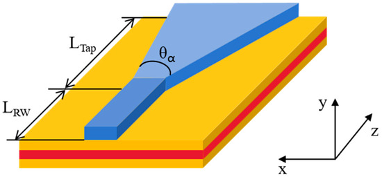
Figure 1.
Schematic diagram of the tapered semiconductor laser structure. (The red part represents InGaAlAs active area, the yellow part represents InGaAlAs waveguide layer, AlInAs confinement layer and InP cap layer, and the blue part represents the current injection region).

Table 1.
Epitaxial structure parameters of the 1.65 μm tapered semiconductor laser.
2.1. Mode Control Theory of Ridge Waveguides
Ridge waveguides represent a typical type of weakly index-guided structure, which confine the optical field by adjusting the lateral refractive index difference. To achieve stable fundamental transverse mode operation in ridge semiconductor lasers, the optimal relationship between the width and depth of the ridge waveguide is generally determined based on the fundamental mode cutoff condition [14,15], expressed as:
where w is the width of the ridge waveguide, λ is the lasing wavelength, neff2 represents the effective refractive index of the ridge mesa, and neff1 denotes the effective refractive index of the etched regions on both sides of the ridge. As indicated by Equation (1), an increase in the ridge width reduces the effective refractive index difference between the ridge mesa and the adjacent etched regions, implying the need for a shallower etch depth beside the ridge. This weakened index contrast diminishes the optical confinement capability of the waveguide and enhances carrier diffusion effects, thereby degrading the device conversion efficiency. Conversely, a narrower ridge width requires a deeper etch to strengthen lateral confinement. However, an excessively narrow ridge may promote higher-order mode excitation, reduce the emitting area, and increase the risk of catastrophic optical damage (COD) at the outcoupling facet [16].
The current injected into the quantum well determines the carrier density within the bound-state quantum well. Through carrier transport in the bulk semiconductor region, the quasi-3D model of the tapered laser is solved in a self-consistent manner by applying the carrier continuity equation and Poisson equation [17]. Under the condition of the effective refractive index approximation, the wide-angle finite-difference beam propagation method (WA-FD-BPM) [18,19] is employed to achieve accurate solution of the optical field. The mode confinement factor is defined as the ratio of the optical power within the active region to the total optical power, which quantifies the degree to which the optical field is confined within the active gain region.
The mode confinement factor (Γ) is closely related to the etching depth of the ridge waveguide laser diode. Typically, a deep etch that penetrates the active region creates a large refractive index step, thereby enabling stronger optical field confinement and a higher Γ value. In contrast, a shallow etch that terminates inside the upper cladding results in a weaker index guiding effect and a reduced Γ value due to the expansion of the mode field. However, there exists a critical trade-off in this relationship: although deep etching can maximize Γ, it simultaneously introduces severe sidewall damage and non-radiative recombination centers, leading to a significant increase in internal loss (α_i). Therefore, there is an optimal etching depth, which is usually achieved by etching into the upper cladding without complete penetration. This approach ensures sufficient optical field confinement while minimizing scattering and absorption losses, maximizing the net modal gain (Γg-α_i).
As shown in Figure 2, the optical confinement of the ridge waveguide strengthens progressively with increasing etching depth, leading to a gradual reduction in the lateral extent of the optical field. The resulting smaller near-field spot size enhances the lateral confinement factor of the mode, thereby increasing the modal gain. Furthermore, deeper etching improves the suppression of carrier lateral diffusion, leading to higher carrier injection efficiency and consequently reducing the threshold current of the device.
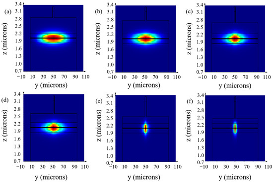
Figure 2.
Optical field distributions in ridge waveguides with different etching depths: (a) 0.5 μm, (b) 0.6 μm, (c) 0.7 μm, (d) 0.8 μm, (e) 0.9 μm, (f) 1.0 μm.
Figure 3 indicates that when the etching depth exceeds a certain value, further increases cause the optical mode to extend toward the substrate in the vertical direction. This reduces the vertical confinement factor and leads to a slight increase in the threshold current. Under such conditions, the device becomes susceptible to thermal lensing effects at higher injection currents, which can excite higher-order modes and significantly degrade the beam quality. Therefore, the optimal etching depth is determined to be 0.8 μm.
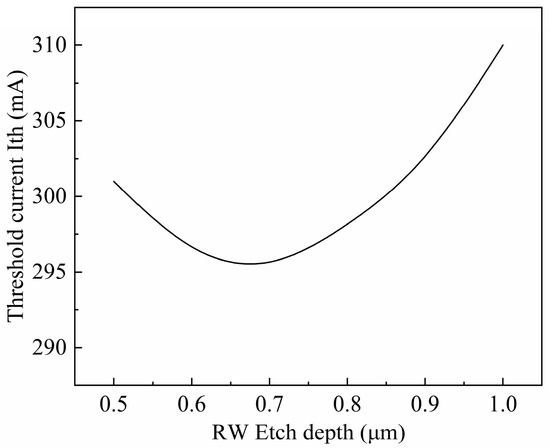
Figure 3.
Dependence of the threshold current on the etching depth of the ridge waveguide in the semiconductor laser.
2.2. Optical Field Propagation Theory in the Tapered Region
To analyze the influence of the taper angle in the tapered gain region on the output power and beam characteristics of the laser, the designed taper angle must be smaller than the free diffraction angle of the fundamental lateral mode. The free diffraction angle of the fundamental lateral mode can be expressed as:
where n is the bulk refractive index, neff denotes the effective refractive index when the ridge waveguide width is W, and neff-n represents the effective index difference as the ridge width approaches infinity, and θp denotes the free diffraction angle of the laser beam.
From Equations (2) and (3), it can be observed that the width of the ridge waveguide structure and its effective refractive index directly influence the free diffraction angle of the fundamental lateral mode [20].
Figure 4 illustrates the optical field distribution under different taper angle conditions. As the taper angle increases, the area of the light-emitting surface gradually expands. In Figure 4a, the optical field is concentrated within a narrow central region, indicating high energy concentration with weak peripheral diffusion. The color bar shows that the high-intensity region occupies a small proportion, suggesting a small beam divergence angle and strong directivity. In Figure 4b, the optical field begins to expand laterally. The area of the central high-intensity region increases, and a distinct transition zone emerges around the periphery. This indicates that the beam starts to diverge yet still maintains relatively strong central energy concentration. In Figure 4c, the optical field distribution broadens significantly. The high-intensity region spreads further, as reflected by the increased proportion of red in the color bar and the expansion of the low-intensity peripheral area. This implies an increase in the beam divergence angle and a more dispersed energy distribution. As the taper angle increases, the confinement capability of the laser’s waveguide structure weakens, leading to the expansion of transverse modes—consistent with the geometric amplification effect of the tapered structure. A smaller taper angle (e.g., 4°) enhances transverse confinement in the tapered waveguide, resulting in a more concentrated optical field. In contrast, a larger taper angle (e.g., 8°) reduces the waveguide’s constraint on higher-order modes, leading to multi-mode oscillation and energy spreading.
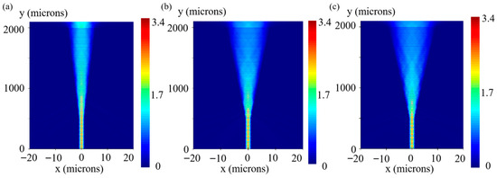
Figure 4.
Distribution of fundamental transverse mode light field under different taper angles: (a) 4°, (b) 6°, (c) 8°.
The effective injection area of the active layer increases relatively, leading to higher waveguide losses and threshold gain in the device. Therefore, devices with smaller taper angles exhibit lower threshold currents and higher slope efficiencies. In contrast, devices with larger taper angles, due to their larger effective injection area and output facet width, possess a higher catastrophic optical damage (COD) threshold, which helps mitigate the occurrence of COD to some extent.
Figure 5 shows the far-field characteristics at taper angles of 4°, 6°, and 8°, respectively. As can be seen from the figure, all three curves exhibit a single-lobed distribution near 0°, indicating that the laser energy is concentrated in the forward emission direction, which is consistent with the typical far-field characteristics of lasers. When the taper angle is 6°, the waveguide structure provides stronger transverse confinement of the optical field, resulting in a small beam divergence angle with energy concentrated in the forward direction (near 0°), forming a narrow and high bell-shaped curve. In contrast, at taper angles of 4° and 8°, the lateral confinement of the waveguide is weakened, leading to broadening of transverse modes during propagation and enhanced diffraction effects. This causes the energy to spread over larger angles, manifesting as a broader curve with elevated intensity at the edges. Furthermore, variations in the taper angle may excite higher-order modes, further broadening the far-field distribution. Therefore, the optimal taper angle is 6°.
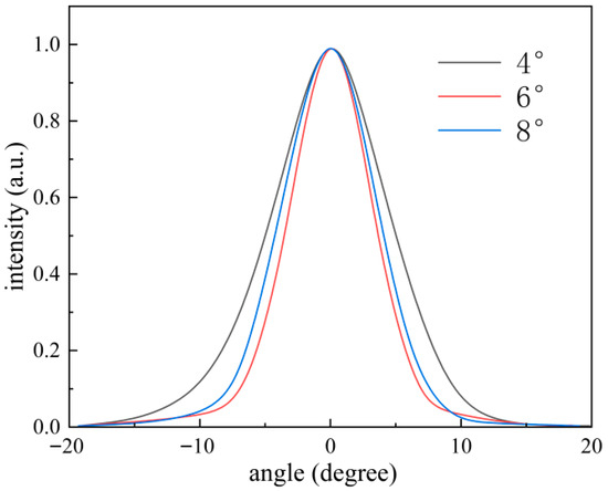
Figure 5.
Horizontal far-field distribution diagrams of the laser under different taper angle conditions.
3. Test Results
All parameters of the tapered semiconductor laser were obtained through the aforementioned design and simulation, including a ridge width of 2 μm, a cavity length of 2000 μm, a 1:3 ratio of the ridge region to the tapered region, an etching depth of 0.8 μm, and a taper angle of 6°. Based on these parameters, the epitaxial wafer was fabricated via metal-organic chemical vapor deposition (MOCVD).
For the growth process, arsine (AsH3), phosphine (PH3), trimethylindium (TMIn), trimethylaluminum (TMAl), and trimethylgallium (TMGa) were used as Group III sources. The doping sources included silane (SiH4), diethylzinc (DEZn), and carbon tetrachloride (CCl4), with high-purity hydrogen serving as the carrier gas. The MOCVD reactor operated at a constant pressure of 50 mbar, with a growth temperature of 720 °C and a V/III molar ratio of 200.
The epitaxial layers were grown sequentially on an n+-doped indium phosphide (n+-InP) substrate, following this order: (1) n+-InP buffer layer. (2) n+-doped aluminum indium arsenide (n+-AlInAs) lower cladding layer. (3) Undoped aluminum gallium indium arsenide (AlGaInAs) lower waveguide layer. (4) AlGaInAs strained quantum wells. (5) Undoped AlGaInAs upper waveguide layer. (6) p+-doped AlInAs (p+-AlInAs) upper cladding layer. (7) p+-doped InP (p+-InP) cladding layer. (8) p+-doped indium gallium arsenide (p+-InGaAs) ohmic contact layer.
The fabrication process of the tapered laser included ultraviolet lithography, wet etching, magnetron sputtering of a SiO2 insulating film, metal electrode preparation, and die packaging. Figure 6 shows the effect diagrams during the fabrication process of five tapered semiconductor laser devices. After the completion of the fabrication process, the following tests were presented.
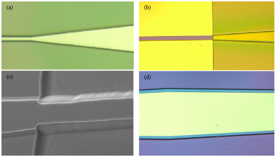
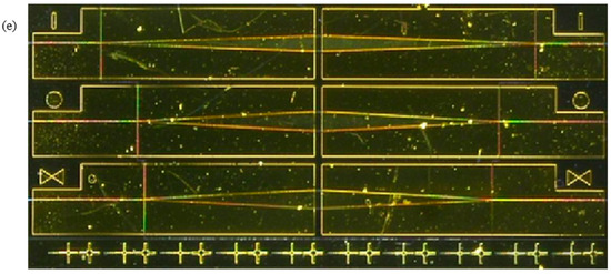
Figure 6.
Fabrication process effect diagrams of the 1.65 μm tapered semiconductor laser: (a) Photoresist morphology under metallographic microscope after the first lithograph. (b) Epitaxial wafer surface morphology under metallographic microscope after wet etching. (c) SEM image of the epitaxial wafer after wet etching. (d) Epitaxial wafer surface morphology under metallographic microscope after the second lithography. (e) Partial surface morphology of the epitaxial wafer after p-side metal electrode preparation.
3.1. Spectral Characteristics
To characterize the emission properties of the device, the output spectrum of the semiconductor laser under continuous-wave (CW) operation was measured using an optical spectrum analyzer (OSA) with a resolution set to 0.1 nm. The measurement was conducted at room temperature, with a scanning range from 1623.16 nm to 1683.16 nm. The results, as shown in Figure 7, demonstrate excellent spectral performance of the semiconductor laser. The dominant lasing peak is located at 1653 nm with a peak power of −26.1 dBm. Most notably, the side-mode suppression ratio (SMSR) reaches 49 dB, indicating outstanding mode selectivity and high single-mode purity. Furthermore, the spectral width at −20 dB is 0.793 nm, reflecting a sharp spectral line and narrow-linewidth characteristics.
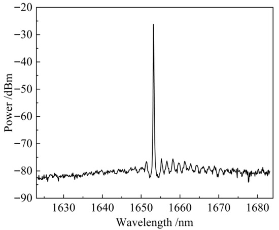
Figure 7.
Spectrum of the tapered semiconductor laser.
3.2. P-I-V Characteristics
After the laser chip was fabricated and packaged, the output performance of the device was tested and analyzed at a controlled temperature of 25 °C. Figure 8 shows the power-current-voltage (P-I-V) characteristic curve of the tapered semiconductor laser. From the test data, the threshold current of the semiconductor laser is determined to be approximately 16.5 mA. When the injection current exceeds the threshold current, the gain generated within the semiconductor laser compensates for the various losses in the laser cavity, resulting in net amplification of photons and enabling the laser to operate in a stimulated emission state, thereby producing laser radiation. At an injection current of 99.8 mA, the maximum output power reaches 19.3 mW, with no significant thermal saturation observed.
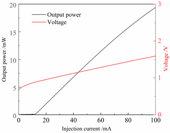
Figure 8.
P-I-V characteristic curve of the semiconductor laser.
3.3. Far-Field Characteristics
Figure 9 shows the far-field distributions perpendicular and parallel to the p-n junction. Measured at 25 °C with an injection current of 30 mA and an output power of 5 mW, the vertical far-field divergence angle (FWHM) is 41.02°, and the horizontal far-field divergence angle (FWHM) is 15.26°. The horizontal far-field profile exhibits a well-defined Gaussian shape, indicating that the fabricated ridge waveguide semiconductor laser operates predominantly in the fundamental transverse mode. This characteristic is beneficial for improving the coupling efficiency between the semiconductor laser and optical fibers.
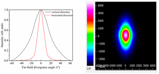
Figure 9.
Far-field distribution and spot profile of the tapered semiconductor laser.
4. Conclusions
This study successfully designed and fabricated a high-performance 1.65 μm tapered semiconductor laser through the integration of waveguide mode theory and beam propagation modeling. Key structural parameters—specifically, a ridge waveguide etching depth of 0.8 μm and a taper angle of 6°—were systematically optimized via numerical simulations. The fabricated device exhibited outstanding performance under continuous-wave operation at 25 °C, achieving a maximum output power of 19.3 mW, a peak emission wavelength of 1653 nm, a spectral linewidth of 0.793 nm, a side-mode suppression ratio (SMSR) as high as 49 dB, along with horizontal and vertical far-field divergence angles of 15.26° and 41.02°, respectively. These results demonstrate the efficacy of the proposed design and offer a viable pathway for developing high-performance semiconductor lasers in the 1.65 μm band, highlighting significant potential for applications in free-space optical communications and lidar systems.
However, several limitations of this work should be acknowledged. First, device performance was evaluated under controlled laboratory conditions, and its stability and reliability have not yet been assessed in practical operational scenarios—such as in the presence of atmospheric turbulence or mechanical vibrations. Second, characterization was primarily conducted at room temperature, lacking a comprehensive analysis of the device’s behavior over an extended temperature range, particularly under extreme high- or low-temperature conditions. Furthermore, the current fabrication process remains unsuitable for large-scale production, with further improvements needed in terms of yield and device-to-device uniformity.
To address these limitations, future research will focus on the following directions: (1) conducting field experiments to evaluate performance robustness in real-world environments; (2) developing temperature-dependent models to extend the operational temperature range and improve thermal management strategies; (3) advancing process standardization and compatibility to enhance manufacturability and reliability; and (4) investigating the integration of this laser into specific application systems, such as mid-range free-space optical communication links and methane gas detection lidar, to fully exploit its technical advantages and practical value.
Author Contributions
Conceptualization, software, data curation, formal analysis, funding acquisition, investigation, writing—original draft, Y.F., W.G. and L.G.; methodology, writing—review and editing, H.J.; software, data curation; writing—review and editing, J.Y. and C.Z.; data curation, Y.F., W.G. and L.G.; writing—review and editing, Y.F., Z.W. and J.T. All authors have read and agreed to the published version of the manuscript.
Funding
This work is supported by Changchun University of Science and Technology Project, (No. KYC-JH-XM-2023-077), Natural Science Foundation of China (NSFC-62275030), Science and Technology Development Plan Project of Jilin Province, China (No. 20240101299JC) and Fund of the Key Laboratory of Laser Technology, China North Industries Group Corporation Limited (No. KLLDT202410).
Data Availability Statement
Data underlying the results presented in this paper are not publicly available at this time but may be obtained from the authors upon reasonable request.
Conflicts of Interest
The authors declare no conflicts of interest.
References
- Chen, L.H.; Yang, G.W.; Liu, Y.X. Development of semiconductor lasers. Chin. J. Lasers 2020, 47, 0500001. [Google Scholar] [CrossRef]
- Wang, K.; Gao, C.; Lin, Z.; Wang, Q.; Gao, M.; Huang, S.; Chen, C. 1645 nm coherent Doppler wind lidar with a single-frequency Er: YAG laser. Opt. Express 2020, 28, 14694–14704. [Google Scholar] [CrossRef] [PubMed]
- Crotti, C.; Deloison, F.; Alahyane, F.; Aptel, F.; Kowalczuk, L.; Legeais, J.-M.; Peyrot, D.A.; Savoldelli, M.; Plamann, K. Wavelength Optimization in Femtosecond Laser Corneal Surgery. Investig. Ophthalmol. Vis. Sci. 2013, 54, 3340–3349. [Google Scholar] [CrossRef] [PubMed]
- Cadroas, P.; Abdeladim, L.; Kotov, L.; Likhachev, M.; Lipatov, D.; Gaponov, D.; Hideur, A.; Tang, M.; Livet, J.; Supatto, W.; et al. All-fiber femtosecond laser providing 9 nJ, 50 MHz pulses at 1650 nm for three-photon microscopy. J. Opt. 2017, 19, 065506. [Google Scholar] [CrossRef]
- Kim, J.W.; Sahu, J.K.; Clarkson, W.A. Efficient single-axial-mode operation of an Er: YAG ring laser at 1645 nm. In Conference on Lasers and Electro-Optics; Optica Publishing Group: Washington, DC, USA, 2008. [Google Scholar] [CrossRef]
- Xian, Q.; Lv, H.; Yao, Y.; Cheng, C.; Zhou, Z. Fabrication and Application of 1653.7 nm Methane Sensor. IEEE Photonics J. 2022, 14, 1552806. [Google Scholar] [CrossRef]
- Wang, Z.H.; Wang, J.H.; Liu, S.N.; Zhang, Y.; Su, P.; Gao, X. Numerical simulation of output characteristics of 980 nm conical semiconductor laser. Chin. J. Lumin. 2022, 43, 275–284. [Google Scholar] [CrossRef]
- Sun, C.M.; Zhu, Z.; Ren, F.Y.; Chen, K.; Su, J.; Xia, W.; Xu, X.G. Study of High-power 808 nm Distributed Feedback Laser Array. Res. Prog. SSE 2024, 44, 72–76. [Google Scholar] [CrossRef]
- Li, Y.; Li, C.; Yuan, C.; Wang, Y.; Wei, X.; Chen, L. High-power 808nm VCSEL arrays for Nd: YAG pumping//Semiconductor Lasers and Applications XIV. SPIE 2024, 13233, 75–82. [Google Scholar] [CrossRef]
- Ouyang, Y.H.; Huang, L.X.; Zhu, Z.L.; Ye, N.; Song, Y.X.; Pan, J.Q.; Zhang, Y.J. Design and Simulation of 1060 nm small divergence collimated semiconductor laser. Res. Opt. Commun. 2025, 5, 53–58. [Google Scholar] [CrossRef]
- Liu, X.; Wu, C.K.; Xue, X.E.; Jarez, M.M.; Wang, J.L.; Su, J.X.; Gao, X.; Fatima, S.; Tian, S.C.; Dieter, B. High brightness 1060 nm Hibbee tapered semiconductor laser. Chin. J. Lumin. 2025, 46, 1310–1316. [Google Scholar] [CrossRef]
- Li, R.X.; Lu, X.M.; Zhao, L.; Zhang, X.Y.; Liao, M.M.; Luo, Q.C.; Zou, P.H.; Qiu, G.S.; Zhang, J. 1060 nm single mode semiconductor laser with high temperature and high slope efficiency. Semicond. Photonics Technol. 2024, 45, 557–560. [Google Scholar] [CrossRef]
- Bendelli, G.; Komori, K. Gain saturation and propagation characteristics of index-guided taperedwaveguide traveling-wave semiconductor laser amplifiers (TTW-SLAs). IEEE J. Quantum Electron. A Publ. IEEE Quantum Electron. Appl. Soc. 1992, 28, 447–458. [Google Scholar] [CrossRef]
- Chang, J.; Xiong, C.; Qi, Q.; Wang, C.; Zhu, L.; Pan, Z.; Wang, Z.; Liu, S.; Ma, X. 1550 nm high-power fundamental transverse mode semiconductor laser and its temperature characteristics. Acta Opt. Sin. 2023, 43, 0714003. [Google Scholar] [CrossRef]
- Zhang, N.; Jing, H.; Yuan, Q.; Lü, J.; Wang, C.; Zhong, L.; Liu, S.; Ma, X. High power 1060 nm tapered laser. Acta Opt. Sin. 2022, 42, 0514002. [Google Scholar] [CrossRef]
- Fu, P.; Zhang, Y.C.; Zhao, T.; Zhao, Y.; Tang, S.; Li, Y.; Han, S.D. Design and fabrication of high efficiency and high-power 976 nm semiconductor laser chips. Chin. J. Lasers 2024, 51, 230896. [Google Scholar] [CrossRef]
- Selberherr, S. Analysis and Simulation of Semiconductor Devices; Springer: Wien, Austria, 1984. [Google Scholar] [CrossRef]
- Hadley, G.R. Multistep method for wide-angle beam propagation. Opt. Lett. 1992, 17, 1743. [Google Scholar] [CrossRef] [PubMed]
- Koch, T.B.; Davies, J.B.; Wickramasinghe, D. Finite element/finite difference propagation algorithm for integrated optical device. Electron. Lett. 2002, 25, 514–516. [Google Scholar] [CrossRef]
- Faist, J.; Capasso, F.; Sivco, D.L.; Sirtori, C.; Hutchinson, A.L.; Cho, A.Y. Quantum cascade laser. Science 1994, 264, 553–556. [Google Scholar] [CrossRef] [PubMed]
Disclaimer/Publisher’s Note: The statements, opinions and data contained in all publications are solely those of the individual author(s) and contributor(s) and not of MDPI and/or the editor(s). MDPI and/or the editor(s) disclaim responsibility for any injury to people or property resulting from any ideas, methods, instructions or products referred to in the content. |
© 2025 by the authors. Licensee MDPI, Basel, Switzerland. This article is an open access article distributed under the terms and conditions of the Creative Commons Attribution (CC BY) license (https://creativecommons.org/licenses/by/4.0/).