1. Introduction
The rapid development of AR technology has been driven by advances in integrated circuit miniaturization, high-performance displays, and digital content creation. By seamlessly merging virtual imagery with real-world environments [
1,
2], AR systems deliver immersive experiences. Among various AR implementation methods, head-mounted displays (HMDs) are widely adopted and mainly consist of micro-display devices and near-eye optical systems. Micro-displays generate virtual images, and optical components project these images into the human eye, integrating them with the real environment [
3,
4]. With the continuous advancement of technology, optical see-through technology has gradually been applied in various fields such as military [
5,
6], industrial [
7,
8], and consumer electronics [
9].
Early HMD designs often employed axial beam splitters based on geometric optical waveguides [
10,
11,
12]. However, this approach makes it difficult to balance performance and portability because the FOV is directly related to the size of optical components, limiting the actual FOV of the device. To address this issue, researchers introduced non-axial aspheric mirrors and freeform optical total internal reflection (TIR) technology. Although these methods have made breakthroughs in expanding the FOV and improving imaging quality, size and non-axial aberrations still affect the user experience. Subsequently, solutions based on micro-lenses [
13], reflective gratings [
14], or computational imaging [
15,
16,
17] further enhanced optical performance. Apple’s head-mounted AR glasses, through advanced screens and non-spherical lens designs, have pushed the system’s smoothness and visual realism to a new level [
18]. However, bulky optical systems remain an important factor hindering their widespread application.
In recent years, diffractive waveguide technology has gradually become a research hotspot [
19,
20,
21,
22]. Compared with traditional bulky AR optical systems, diffractive waveguides have achieved a good balance among FOV, frame size, appearance design, and mass production [
23,
24,
25,
26,
27,
28]. Its core principle is to couple the light of a micro-projector into the waveguide plate and then project the image into the human eye through the exit area. The overall performance of the waveguide is closely related to the optimization of the grating groove shape and the waveguide layout. Through precise design and optimization, efficient and uniform optical transmission and imaging effects can be achieved. However, as a common optical phenomenon in diffractive waveguides, the rainbow effect occurs when ambient light is diffracted by the grating on the waveguide surface and then dispersed into bright areas similar to a rainbow, thus significantly reducing the visual experience. Suppressing the rainbow effect has become one of the key challenges to improving the performance of AR glasses and achieving higher market acceptance [
29,
30,
31].
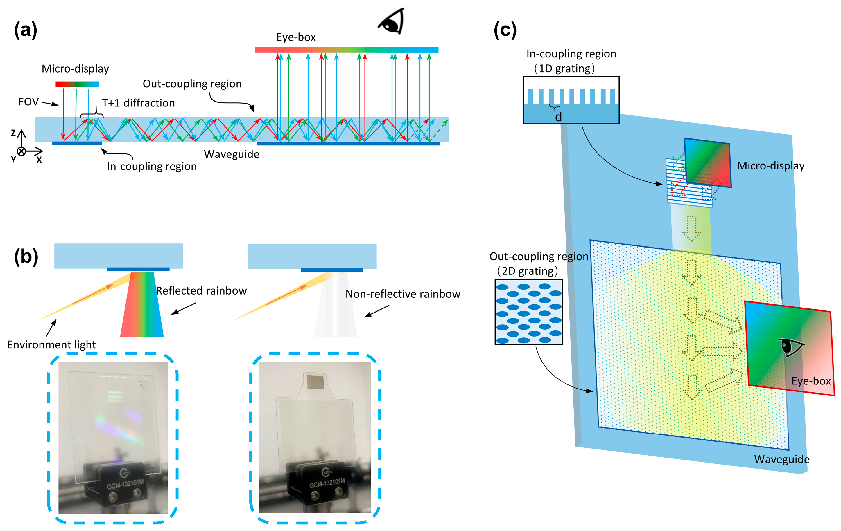
This study proposes novel lightweight single-layer optical waveguide AR glasses with characteristics of a large FOV, complete suppression of the rainbow effect, and high definition. The schematic diagram of the AR lens is shown in
Figure 1a,c. To achieve a rainbow-free AR optical waveguide, we construct PL theory for the outcoupling optical waveguide based on the direction cosine space and use high-refractive-index SiC material to achieve wide-spectrum, large-field imaging. The main advantage of SiC is its higher refractive index of ~2.7, enabling a full-color FOV exceeding 70° in a single waveguide layer, and lower density of approximately 3.2 g cm
−3, contributing to a reduction in weight—a critical advantage for everyday wearable AR devices. The input grating of multi-layer materials adds an abrupt phase on the waveguide surface, realizing flexible adjustment of the energy of 0R, 1R, and −1R diffraction orders. The diffraction efficiency of the input grating is significantly enhanced by optimizing the height of the grating and the thickness of the silver (Ag) film. Additionally, adjusting the long and short axes of the two-dimensional grating unit, along with the structural thickness, improves angular uniformity across different diffraction orders. The experimental results in
Figure 1b further verify that our AR glasses successfully suppress the rainbow effect within the designed FOV.
2. Design and Principle
In augmented reality waveguide displays, the rainbow effect is a significant problem that severely hinders the viewing experience. This problem is caused by color dispersion due to the diffraction of ambient light by the output coupler when external light directly irradiates the output grating area. To address this issue and simplify the design process of diffractive waveguides, we propose a new design method: PL theory. This method optimizes grating parameters more intuitively and efficiently, reducing the impact of the rainbow effect while improving the overall performance of the display system. Since the light conduction process of the output grating of the waveguide is similar to that of the input grating, only higher-order diffracted light is likely to couple out of the waveguide and enter the human eye for imaging. Taking the normal of the waveguide interface as a reference, taking the diffracted light of order−1 as an example, the grating equation can be expressed as
In the formula, the incident angle is
, the diffraction angle of the −1-order is
, the refractive index of the incident medium air
= 1, the refractive index of the waveguide medium is denoted as
n, and
d is the grating period. Obviously, for light transmission, TIR must occur (i.e.,
), and
, and the working wavelength
of the waveguide is located in the RGB band. Based on the above boundary conditions of the diffractive waveguide, the following can be obtained as
where
is the maximum wavelength of the light beam emitted by the optomechanical device, usually 650 nm for red light, and
is the characteristic wavelength of blue light in natural light, usually 450 nm. Equation (2) indicates that the grating period is related to the FOV angle range of the optomechanical device, and the refractive index of the waveguide.
Figure 2a depicts the real-space parameters of the waveguide in the exit pupil area, where the waveguide length is
L, the width is
W, the observation distance of the human eye is
D, the horizontal FOV angle is
θH, and the vertical FOV angle is
θV. In the
k-diagram, the boundaries of the exit pupil area in the real space are transformed into four pink rectangles with corners
a,
b,
c, and
d. Their coordinates are
,
,
, and
respectively, as shown in
Figure 2b. Considering that ambient environmental light with a wavelength of
λ is obliquely incident on the exit pupil area, it is equivalent to an inner circle with a radius of 1 moving a distance of
λ/
d along the direction of the outcoupling grating vector, where
d is the period of the exit pupil grating. At this time, if the moved circle overlaps with the see-through FOV area, rainbow patterns may be observed in the corresponding area of the waveguide. To ensure that there is no rainbow diffraction within the entire wavelength band, combined with the total reflection relationship (Equation (2)), the grating period
d needs to satisfy
where
is the maximum angle between the input light ray and the normal direction of the plane where the waveguide substrate is located, that is, the maximum viewing angle of the human eye. It can be derived from the formula
, where
L is the length of the outcoupling area and
D is the size of the exit pupil distance.
In the design of a two-dimensional diffractive waveguide, a precise relationship is maintained between the period of the one-dimensional input grating and the periods of the two-dimensional output grating. To achieve continuous light transport and expansion, the output grating is structured in an elliptical pattern such that the ratio of the horizontal period, dx, to the vertical period, dy, is . Furthermore, to maintain consistency between the coupled-in and coupled-out beams, the sum of the grating vectors must be zero. This condition necessitates that dx:d = 2:1.
To achieve a high-efficiency one-dimensional input grating, we employ a SiC etching process with a Ag-plated film and a grating structure with vertical channels. A SiC layer with a high refractive index is selected as the waveguide material to achieve effective steering of RGB light and expansion of the exit pupil. Meanwhile, in the SiC waveguide, ambient light can be diffracted at larger angles, and most of it is guided outside the line of sight of the human eye, thus effectively suppressing the rainbow effect.
In the simulation settings, the refractive indices of the waveguide substrate and the grating structure are both set to 2.6. All grating regions adopt a binary grating structure with a period
d = 295 nm.
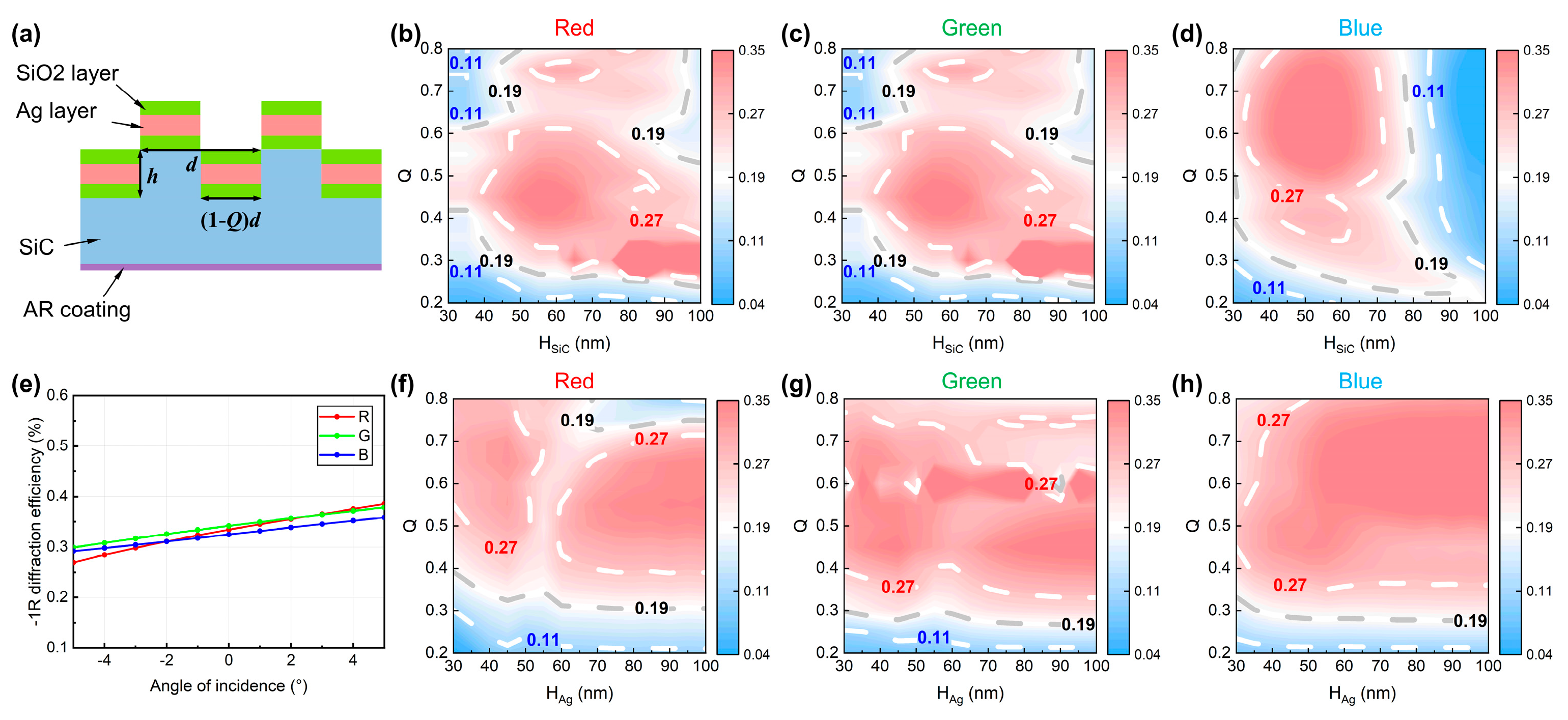
Figure 3a is a cross-sectional schematic diagram of the waveguide input area. The designed structure includes an area etched to a depth of
h on the SiC substrate, on which a silicon dioxide (SiO
2) layer, a Ag layer, and a SiO
2 layer are deposited in sequence.
Figure 3b–d show the diffraction efficiency cloud diagrams obtained by changing the etching depth (
h) and duty cycle (
Q) of the input grating on the SiC substrate. The results show that for red, green, and blue light, the maximum efficiency is close to 0.4, and there is an overlap in the optimal
Q and etching depth regions for different colors, facilitating the selection of the most suitable parameters.
Figure 3f–h further analyze the influence of adjusting the thickness of the SiC substrate (
HSiC), the thickness of the Ag layer (
HAg), and the
Q on the diffraction efficiency. The results indicate that altering the thickness of the Ag layer has a relatively minor impact on overall efficiency, whereas modifying the
Q reveals significant efficiency variations across different regions, with high diffraction efficiency values concentrated within the
Q range of 0.5–0.6. Based on the above analysis, the final design parameters of the input grating are determined as follows: height
h = 50 nm,
Q of 0.5, and coating thicknesses of SiO
2 Ag and SiO
2 in sequence, with values of 20 nm, 100 nm, and 20 nm, respectively.
After adapting to the above parameters, the diffraction efficiency of −1-order was further scanned.
Figure 3e shows the curves of the −1-order diffraction efficiency of RGB light with the incident angle when the incident light is circularly polarized. When the incident angle varies from −5° to 5°, the average coupling efficiency of the center wavelengths of RGB colors exceeds 30%, showing good field uniformity. The final design makes the coupling efficiencies of all angles and colors relatively close, enabling the output of a complete full-color image throughout the entire FOV range.
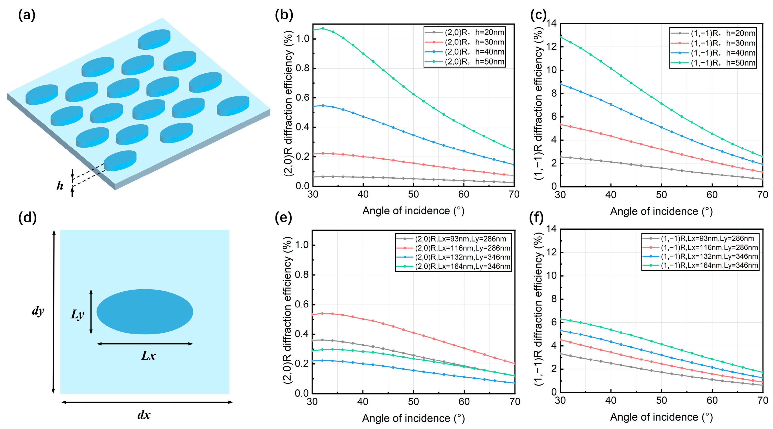
Optimizing the angular uniformity of the two-dimensional outcoupling grating at the micro-scale is a crucial step in enhancing the performance of optical waveguides. The shape of a single structure is designed as an ellipse, as shown in
Figure 4a,d. Based on the PL theory, the period lengths of the unit structure are set as
dx = 590 nm and
dy = 341 nm, respectively. To achieve effective pupil expansion and beam emission, Lx and Ly are set as 346 nm and 132 nm, respectively. The diffraction efficiency under the diffraction orders (1, −1) R and (2, 0) R is measured, and the outcoupling uniformity at different angles is deeply analyzed. As shown in
Figure 4e,f, when the long axis of the outcoupling grating is 346 nm and the short axis is 132 nm, while ensuring high transmission efficiency of the outcoupling grating at the (1, −1) R-order, the (2, 0) R-order has a more uniform pupil efficiency. As shown in
Figure 4b,c, when the incident light angle is in the range of 30° to 70°, the diffraction efficiencies of the (1, −1) R and (2, 0) R-orders decrease successively with the increasing of e incident angle and increase successively with the increaseing of the grating height. To make the diffracted light expand and outcouple more uniformly in the outcoupling grating area, we select the height of the outcoupling grating to be 30 nm. Through the above optimization methods, we achieve a more precise adjustment of the diffraction efficiency, thereby improving the outcoupling performance of the two-dimensional grating.
3. Fabrication and Measurements
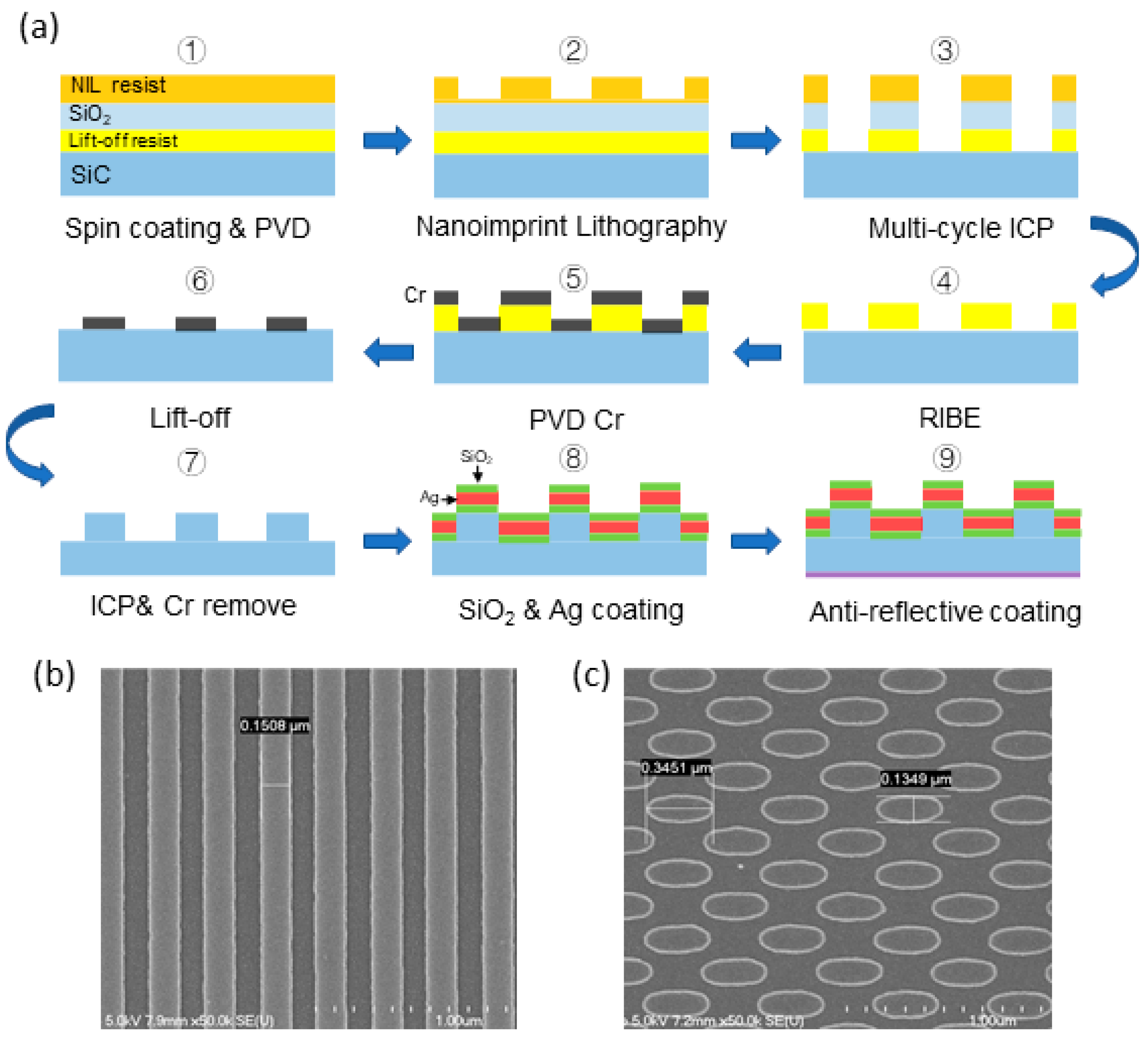
The waveguide section is fabricated using lithography and nanoimprint techniques, with SiC material selected as the base for the waveguide and grating structures. The manufacturing process of the waveguide is illustrated in
Figure 5. Firstly, a photosensitive resin is spin-coated onto the SiC substrate, and SiO
2 and Lift-off photoresist are deposited using physical vapor deposition (PVD) technology. Subsequently, the nanoimprint technique is employed to transfer the pattern onto the photoresist, forming nanostructures. Then, multi-cycle inductively coupled plasma (ICP) and reactive ion beam etching (RIBE) techniques are utilized to define the outcoupling region and etch the gratings in the incoupling region, respectively. After etching, the photoresist layer is removed via Lift-off technology to obtain the SiC optical waveguide. Next, a SiO
2 layer and a Ag layer are coated to enhance optical performance, followed by the application of an anti-reflection coating at the bottom of the waveguide to optimize light transmission.
Figure 5b,c present the scanning electron microscope (SEM) images of the processed waveguide. It can be observed that the elliptical micropillar profiles of the outcoupling region after etching are clear, and the periodicity is well-preserved with high precision, ensuring a high-resolution display effect. Although there is a slight rounded corner difference between the actual grating and the theoretically designed rectangular grating at the corners, this minor roughness is within an acceptable range and does not affect the overall optical performance of the system. The manufacturing process of the grating waveguide involves creating a wafer master using electron beam lithography technology, followed by large-scale production using nanoimprint technology. Finally, the replicated waveguide layer is sealed and cut into the final waveguide products. The structural size parameters of the waveguide are as follows: the waveguide thickness is 0.5 mm, the incoupling region dimensions are 8 mm × 6 mm, and the outcoupling region dimensions are 33.8 mm × 28.6 mm. This structural design effectively improves light transmission efficiency and ensures that the optical performance of the waveguide meets the requirements of AR devices. Through this process, the dimensional and structural accuracy of the waveguide is ensured, further enhancing optical performance. This process combines efficient nanoimprint technology and precise etching techniques, ensuring high consistency of the waveguide structure and stability of optical performance. Additionally, the application of SiC material further enhances the light transmission capability of the waveguide. Moreover, due to its excellent heat resistance and wear resistance, the durability of the product is greatly improved. This novel waveguide manufacturing process provides a feasible solution for high-quality display and large-scale production in AR display technology.
Based on the previous theoretical and simulation results, we fabricated a single AR waveguide lens and measured its optical performance.
Figure 6a,c shows the appearance of a single ultra-thin waveguide, which realizes a large-aperture outcoupling area with a length of 36 mm and a width of 30 mm. The weight of a single lens is 2.12 g, which conforms to the advantages of weight and comfort of the finished glasses brought by the single-layer design. We loaded an image carrying RGB three-color wavelength letters on a single lens to test its display performance. The colors are pure, and the details are well-reproduced. The aviation engine model in the background is visible, achieving the effect of augmented reality.
On this basis, we integrated two lenses into a pair of AR glasses, which carry a micro-display unit internally. It realizes an exit pupil distance of 20 mm and a diagonal FOV of 55°, providing a large FOV and high imaging quality. The letter effects are displayed on the left and right sides, respectively, fully demonstrating the stability of the system in terms of image display quality, contrast, and color restoration. In addition,
Figure 6e,f show the performance of the glasses in practical applications. After loading high-resolution images, the device can accurately restore color images and text information, and the resolution performance is excellent. The display effect is very clear, and the details are rich. The above experimental results show that this device not only performs excellently in terms of imaging effect, optical efficiency, and wearing comfort but also can effectively suppress the rainbow effect in traditional display devices.
The optical performance of the waveguide, including luminance uniformity and modulation transfer function (MTF) across the field of view, was characterized using a Radiant imaging measurement system equipped with an AR/VR lens replicating the human pupil. When tested with a 50° medium-intensity digital light processing (DLP) light engine, the brightness of the waveguide is 1100 nits, the modulation transfer function (MTF) is 0.7 horizontally and 0.65 vertically, and the FOV is 55°. The transmittance of the waveguide is 87%. The actual color performance captured in photographs is shown in
Figure 6, demonstrating excellent color uniformity. Thanks to the high optical energy efficiency of the waveguide and the high brightness of the projector, the SRG waveguide display module can operate normally under outdoor conditions. The optical engine uses a DLP projector provided by Coretronic, featuring a resolution of 1280 × 720p, a 50° FOV (diagonal), a contrast ratio of 300:1, and an RGB LED light source.
4. Conclusions
The AR glasses based on the novel SiC single-layer diffractive optical waveguide proposed in this paper successfully addressed the common issues in traditional AR optical display technologies, such as field-of-view limitations, rainbow effects, and bulky equipment. Through the innovative design of high-refractive-index SiC material and surface-relief gratings, the system achieves efficient optical transmission over a large FOV. It can effectively suppress the rainbow effect caused by ambient light, significantly enhancing the visual experience. The optimized grating design not only improves the light coupling efficiency but also ensures the clarity of image display and the accuracy of color reproduction. The experimental results verified the excellent performance of this system in various environments, with stable and high-quality display effects, capable of providing clear and delicate images even in complex backgrounds. Furthermore, the lightweight design of the device offers excellent wearing comfort, meeting the demands of prolonged use, and features high brightness and transmittance, making it suitable for outdoor applications. This research paves the way for future optimizations in AR optical display technologies in terms of display performance, comfort, and operability, holding broad application prospects.
While this study demonstrates significant improvements in FOV, rainbow suppression, and uniformity through the proposed SiC-based diffractive waveguide architecture, several promising pathways remain for further enhancing performance. Future work will explore the integration of metasurfaces to mitigate chromatic aberration—a fundamental bottleneck in broadband waveguide displays. Metasurface-based optical elements exhibit exceptional phase control capabilities across the visible spectrum, providing a viable route toward achromatic and highly efficient diffractive optics. Additionally, the development of hybrid grating structures, combining geometric and meta-grating features, may offer new degrees of freedom in light manipulation, further increasing diffraction efficiency and angular bandwidth.
Another compelling direction involves the application of inverse-design and computational optimization methods to realize multi-layer and multi-functional grating configurations that are otherwise challenging to achieve with conventional design frameworks. Such approaches could facilitate more compact optical systems with improved luminance uniformity and wider eyebox. We also envision the incorporation of dynamic tuning mechanisms, such as electrowetting or phase-change materials, to enable adaptable diffractive optics for real-time response to varying ambient conditions or user preferences. These emerging technologies, supported by recent advances in nanofabrication and computational imaging, hold considerable potential to push the boundaries of augmented reality displays toward truly immersive, visually comfortable, and consumer-ready devices.


