Communication

Enhanced Performance of High-Power InAs/GaAs Quantum Dot Lasers Through Indium Flushing

by
Deyan Dai
1,2,
Hanqing Liu
1,2,
Xiangjun Shang
1,2,
Shizhuo Tan
1,2,
Qiaozhi Zhang
1,2,
Chengao Yang
1,2,
Dongwei Jiang
1,2,
Xiangbin Su
1,2,*,
Haiqiao Ni
1,2,* and
Zhichuan Niu
1,2,3
1
Key Laboratory of Optoelectronic Materials and Devices, Institute of Semiconductors, Chinese Academy of Sciences, Beijing 100083, China
2
Center of Materials Science and Optoelectronics Engineering, University of Chinese Academy of Sciences, Beijing 100049, China
3
Hefei National Laboratory, Hefei 230088, China
*
Authors to whom correspondence should be addressed.
Photonics 2025, 12(1), 62; https://doi.org/10.3390/photonics12010062
Submission received: 14 November 2024 / Revised: 29 December 2024 / Accepted: 8 January 2025 / Published: 13 January 2025

Abstract

:
InAs/GaAs quantum dots (QDs) appear promising for optoelectronic applications. However, the inhomogeneous broadening caused by natural strain and the non-uniform size distribution deteriorates the device performance based on multi-stacked QD layers. In this study, In-flush was incorporated during the epitaxy, and the photoluminescence (PL) linewidth was significantly narrowed to 26.1 meV for the flushed sample and maintained to 27.3 meV for the unflushed sample. The flushed sample shows better device performance in threshold current (0.229 to 0.334 A at 15 °C), power (1.142 to 1.113 W at 15 °C), and characteristic temperature (51 to 39 K in the range of 55~80 °C) compared with the unflushed sample.

1. Introduction

Self-assembled InAs/GaAs quantum dots (QDs) have attracted much attention due to their δ-like density of energy states, and their carrier states are spatially confined in this three-dimensional atomic-like structure. These unique properties make high-density QDs highly promising as a gain medium in laser diodes [1], superluminescent diodes [2], semiconductor optical amplifiers [3], and other advanced applications [4]. Recently, InAs/GaAs 1.3 μm QD lasers, grown by molecular beam epitaxy (MBE), have demonstrated impressive characteristics such as high-temperature stability, a high modulation rate, high differential gain, and a low threshold current, which allow devices to operate without extra cooling equipment [5,6,7]. However, the inhomogeneous strain [8] and dot size distribution of QDs, grown via the Stranski–Krastanow (S-K) growth mode, can naturally display wide spectra when used as an active region, and the full-width at half-maximum (FWHM) of the photoluminescence (PL) spectrum of the QD ground state (GS) is strongly affected by their shape, size, and material composition.
Typically, for a QD density higher than 4 × 1010 cm−2 with high quality and uniformity, the PL line width is approximately 27 to 35 meV [9,10], representing its inhomogeneous broadening characteristics brought by the S-K growth mode. However, by properly controlling growth parameters, including the QD growth rate [11], wetting layer (WL) composition, growth temperature [12,13], and thickness of capping layers [14], QDs can be modulated and result in a uniform distribution reflected by the narrowing of PL lines [15]. Several studies have employed in situ morphology modulation techniques, such as the so-called indium flush (In-flush), to promote QD uniformity and reduce PL broadening. Wasilewski et al. introduced In-flush in a compact stacked vertical coupled QD layer structure and a sharp PL line was acquired, but the uncoupled QDs along the growth direction were mentioned to be rather smaller due to noticeable PL broadening with lateral size expansion in successive layers. Further investigation [16] revealed that both lateral and vertical size distributions could be controlled via In-flush in an uncoupled system. Recently, a rather narrowed PL line width of 27.4 meV has been achieved in multi-stacked QD layers [17], and the MBE growth of high uniformity low-density QDs was also acquired through In-flush [18,19]. However, similar morphology tuning for high-density QDs [20], particularly in uncoupled vertical stacked QD layer structures [11,16] used as the gain medium, remains underexplored.
In this work, an uncoupled multi-stacked QD layer structure was optimized by in situ annealing after capping with InGaAs and GaAs layers, and a narrowed PL line width of 26.1 meV was acquired after introducing the In-flush procedure in this high-density QD sample, while the line width was 27.3 meV for the sample without flushing. Despite the observed blueshift in PL spectra, the unexpected lateral size expansion was not observed in the cross-sectional TEM images of the five-stacked structure. In addition, the histogram statistics of the AFM results further confirmed the enhanced size uniformity after introducing the thermal flushing treatment. Based on the optimization above, the QD laser consists of five-stacked flushed layers that exhibited significant performance improvements, including a reduction in the threshold current (0.334 to 0.229 A at 15 °C), a narrower electroluminescence (EL) spectrum line width at room temperature under an injection current density of 250 A/cm2 (1.64 to 1.41 meV at 15 °C), and the promotion of output power (1.113 to 1.142 W at 15 °C) when the injection current is 4 A compared with the laser without In-flush. The output power of the flushed sample also achieved an output power exceeding 300 mW under continuous wave (CW) operation at 80 °C, demonstrating enhanced thermal stability relative to the untreated sample.

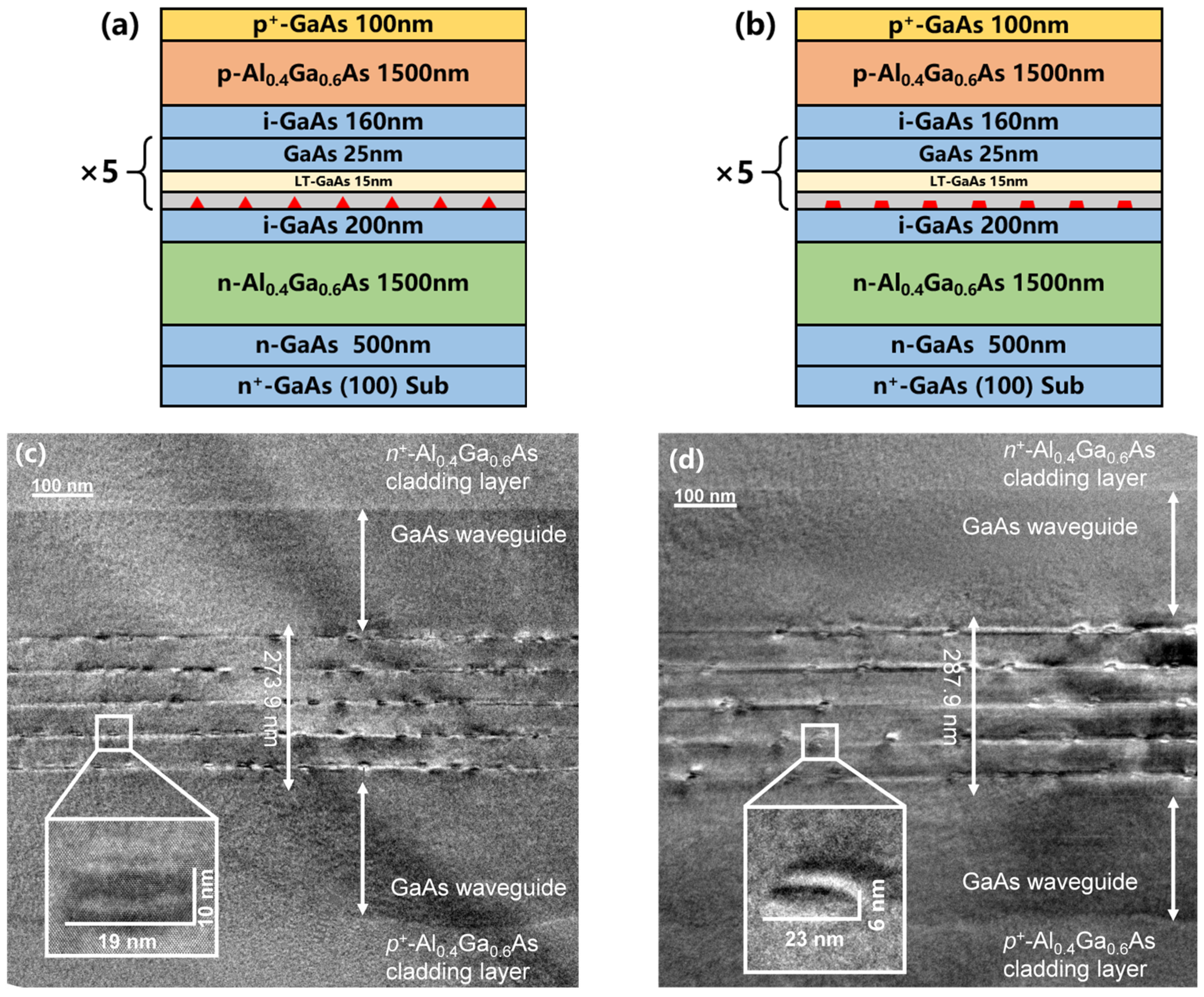
2. Materials and Methods

The InAs/GaAs QD were grown by an MBE (Veeco Gen 930, Saint Paul, MN, USA) on n-type GaAs (100) substrates. To measure the PL spectrum, samples consisting of three-stacked QD layers were grown. Substrates were treated at a high temperature to remove the native oxides by thermal flashing for 30 min under arsenic atmosphere protection. After the deoxidation process, a 30 nm GaAs buffer layer was grown to flatten the surface. Epitaxy was then performed with an In deposition rate of 0.1 ML/s, and the deposition amount was maintained to 2.3 ML to form high-density self-assembled QDs.
For the unflushed sample, a 5 nm in thickness In0.13Ga0.87As layer was deposited on the QDs to release the native strain, and the 40 nm GaAs spacer layer consisting of a 15 nm low-temperature (LT) GaAs and a 25 nm GaAs layer was grown to spatially separate multi-stacked QD layers, as shown in Figure 1a,b. Similarly, for QDs undergoing the in situ In-flush procedure, a 3 nm In0.15Ga0.85As strain-release layer (SRL) was grown, following the application of a 2 nm GaAs capping layer on the SRL for protection. The In-flush procedure was then performed after raising the substrate temperature to the In desorption point which was 20~25 °C higher than the QD formation temperature (approx. 530~535 °C), and most of the resident In on the surface was removed after treating with thermal flushing for 190 s. After that, a 40 nm GaAs spacer layer was grown on the same unflushed sample.
To evaluate the electrical properties, including the P-I-V curves and EL lasing spectrum, two kinds of p-i-n devices, consisting of five-stacked InAs/GaAs QD active regions based on the above epitaxial structures, were grown. The active region was sandwiched between a symmetrical layer structure schema, including a 200 nm waveguide layer and a 1500 nm Al0.4Ga0.6As cladding layer. Details of the epitaxial structures are available in ref. [5], and a schematic illustration of the complete device structure is shown below. Furthermore, cross-sectional TEM images are provided in Figure 1c,d; unflushed QDs with a pyramid shape have a lateral width of 19 nm and a height of 10 nm. For the flushed QDs with a truncated shape associated with the “trimmed” QDs in Figure 1b, the width and height are 23 nm and 6 nm, respectively. It is observed that the density distribution of flushed QDs is less than that of the unflushed sample, indicating that the In-flush procedure affects surface morphology.

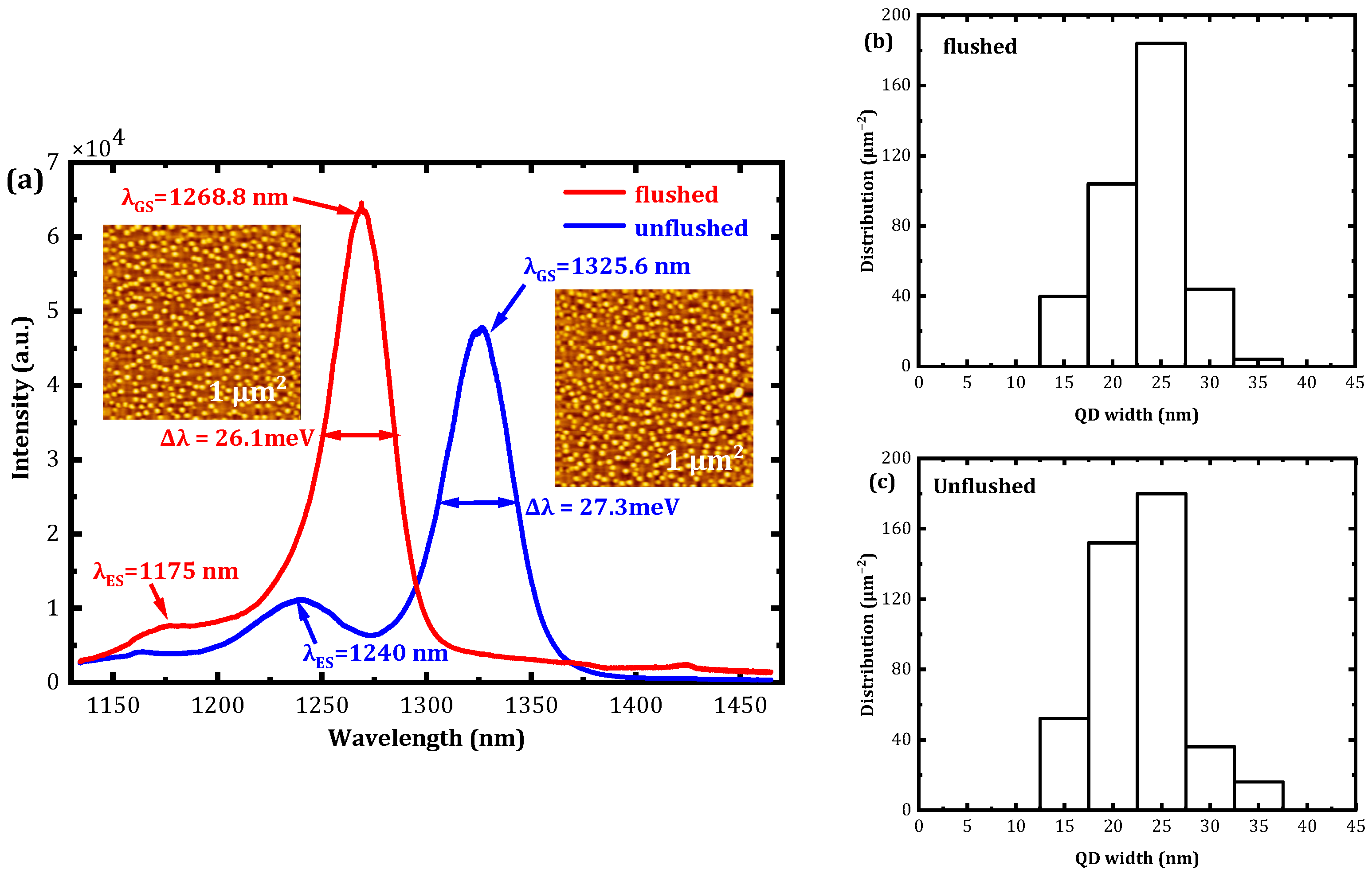
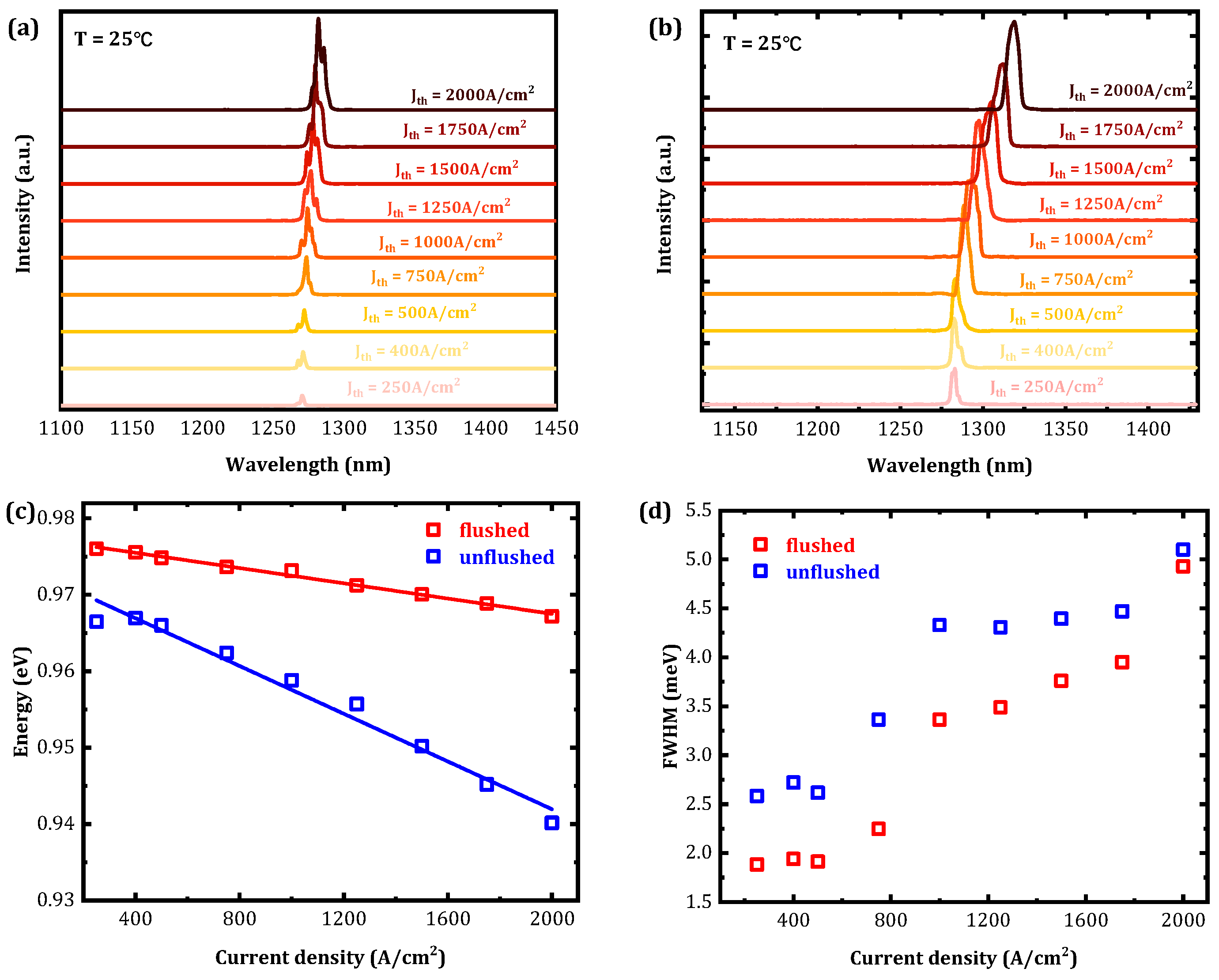
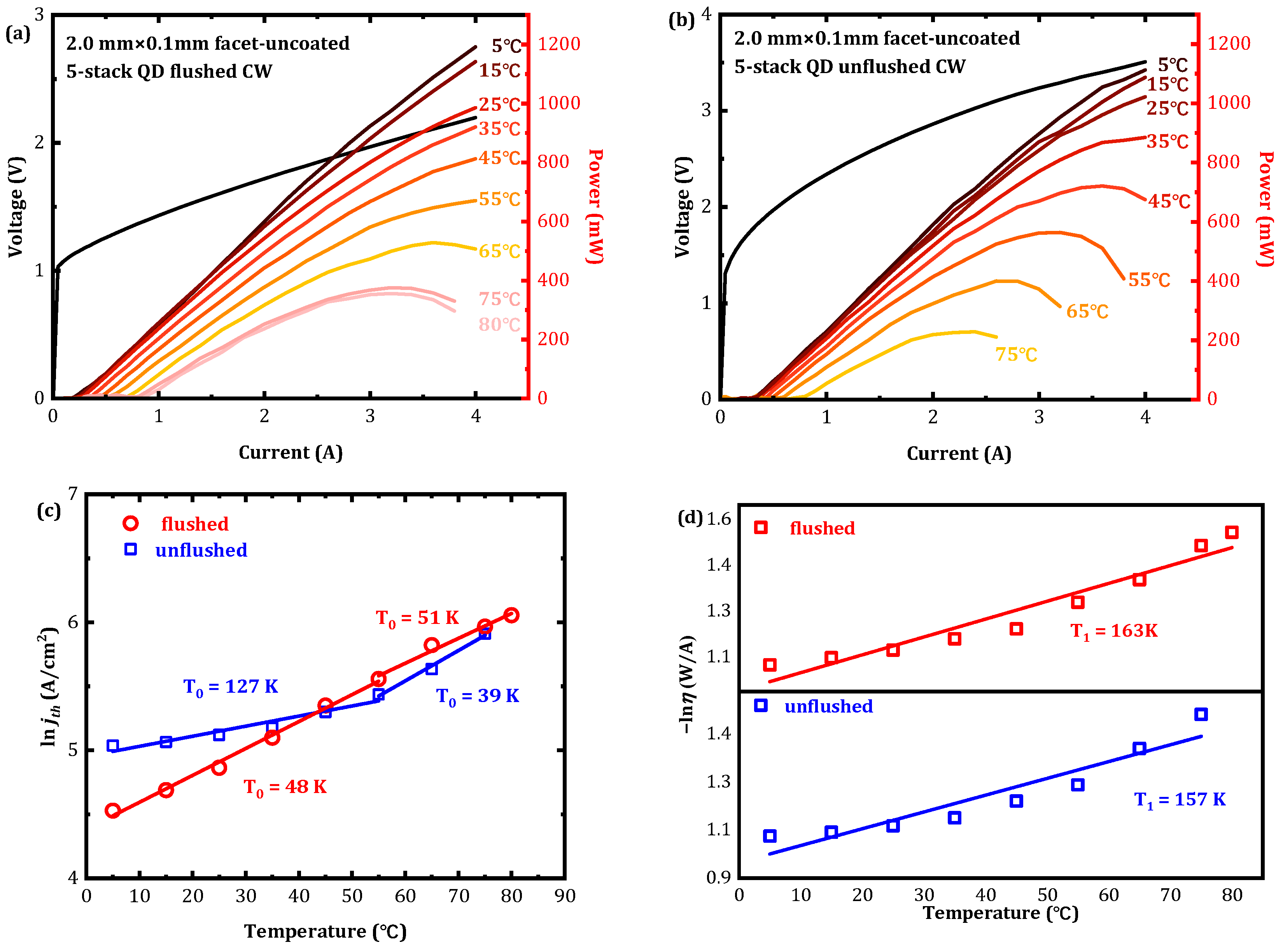
3. Results and Discussion

As depicted in Figure 2a, the room-temperature PL spectra of the two samples are shown in a red curve and a blue curve. The emission center wavelengths of the flushed and unflushed samples are 1268.8 nm and 1325.6 nm, respectively. The PL spectrum of the flushed sample exhibits a higher intensity and a narrower FWHM of 26.1 meV compared to the unflushed sample with a corresponding value of 27.3 meV. The 1 μm2 AFM images are also included in Figure 2a to represent the morphology properties in size uniformity and distribution. For the sample treated without thermal flush, the QD density was approximately 5 × 1010 cm−2, while the flushed sample displayed a slightly lower density of 4.5 × 1010 cm−2. The width size distribution statistics were derived from the AFM images to compare the uniformity. The flushed QDs predominantly ranged in size from 22 to 25 nm, whereas the unflushed QDs were distributed between 19 and 22 nm. Moreover, QDs with sizes larger than 35 nm were more frequently observed in the histogram statistic of Figure 2c, indicating a bimodal size distribution, and the In clusters observed in the AFM images led to the broadening of the PL spectra. In this case, the thermal flush treatment can not only significantly improve size uniformity and eliminate the extra surface In caused by a higher deposition rate, but it can also narrow the line width due to the greater confinement of carriers in the dots [15]. In addition, the emission wavelengths of the flushed QDs shift toward shorter wavelengths, causing a blue shift in peak position in the red curve. This can be attributed to the reduction in height along the vertical direction and In/Ga interdiffusion between QD and the surrounding barrier layers after thermal flushing [21].
In addition, it was observed that the central emission wavelengths of GS and the first excited state (ES1) of these two samples exhibit different energy separations. The flushed sample has a much wider energy gap between GS and ES1 of approximately 78 meV (93.8 nm), compared to 64.5 meV (85.6 nm) in the sample without flushing. The thermal carrier leakage from GS to ES1 or other higher energy states was suppressed due to this separation, which effectively reduced the temperature sensitivity of the lasing threshold under continuous wave operation [22,23].
Based on all the device structures we grew, the wafers were then fabricated into ridge waveguide lasers by standard lithography and dry etching, without any coatings on either end facet. The ridge width of the lasers was 100 μm, and the cavity length was 2 mm.
Figure 3 compares the single-side power–current (P-I) curves of the flushed and unflushed lasers under CW current mode operation at 15 °C. It can be seen that the threshold current of the flushed laser was as low as 0.229 A, which was much smaller than that of the unflushed laser (0.334 A). The corresponding threshold density for the flushed laser was only 114.6 A/cm2 (22.92 A/cm2 per QD layer), whereas for the unflushed laser, it was 166.8 A/cm2 (33.35 A/cm2 per QD layer). In addition, the emission spectrum was also acquired at 15 °C for these two lasers and is shown in the inset. The flushed sample was lased at a wavelength of 1265 nm under an injection current density of 120 A/cm2, and the unflushed sample was lased at a peak wavelength of 1277 nm under an injection current density of 170 A/cm2. The spectrum line width for the flushed sample was as low as 1.41 meV, which is smaller than that of the unflushed sample (1.64 meV).
To evaluate the emission performance, the injection current-dependent EL spectral characteristics acquired at room temperature are represented in Figure 4a,b. The peak wavelength shifts from 1270 nm at a current density of 250 A/cm2 to 1281 nm at 2000 A/cm2 for the flushed QD laser, whereas for the unflushed QD laser, it shifted from 1283 to 1319 nm at the same injection current density range. When the injection current is above the threshold current, the temperature of the p-n junction increases with the increase in current density, consequently resulting in a redshift in peak wavelength. The wavelength of the flushed QD laser only shifts 11 nm when the injection current density octuples from 25 to 2000 A/cm2; however, this value was 36 nm for the unflushed QD laser, representing a poor ability to resist redshift with an increase in temperature. Furthermore, the wavelengths and line widths are extracted to compare the emission performance in Figure 4c. Through the linear fitting of the wavelength shift tendency, the flushed sample shows a significantly flatter slope trend, with a linear slope of −0.5 × 10⁻⁶ compared to the unflushed sample with a slope of −1.6 × 10⁻⁵, which demonstrates a significantly better anti-redshift ability compared to the unflushed one.
The spectrum line widths of these two samples are shown in Figure 4d, with both emission spectra exhibiting broadening with an increase in current density. However, the flushed sample shows significantly lower spectrum broadening compared to the unflushed sample. The maximum line width was only 4.93 meV for the flushed sample but 5.1 meV for the unflushed sample at a current density of 2000 A/cm2. In conclusion, when the injection current is above the threshold current, the flushed sample demonstrates a better three-dimensional quantum confinement effect in the QD, and the injected electrons and holes were stable in the active region, with less carrier leakage or thermal escape compared to the QDs without the thermal flush treatment.
The electrical properties of these two lasers were then measured, and they are represented in Figure 5. The P-I curves shown in Figure 5a,b were measured at temperatures ranging from 5 to 80 °C under a CW current mode with the assistance of a temperature control thermoelectric cooler (TEC) module. Both laser diodes exhibit excellent high-temperature performance; the output power for the flushed QD laser exceeds 1200 mW at 5 °C, with a threshold current as low as 0.17 A. Although visible thermal degeneration occurred at 65 °C as the injection current increased, the output power still exceeded 300 mW at 80 °C, with a threshold current of 0.8 A. For the unflushed QD laser, the output power was as high as 1113 mW at 5 °C, when the threshold current is 0.32 A and the maximum output power at 75 °C exceeds 200 mW. Thermal degeneration was shown at 45 °C, with apparent power saturation, whereas for the flushed sample, this occurred at 65 °C.
In addition to the P-I performance, the temperature-dependent characteristics of the threshold current density (jth) and slope efficiency (η) were extracted from the P-I curves to further compare the thermal stability. The characteristic temperature T0 and the slope characteristic temperature T1 were determined using the equations proposed in reference [24]. Figure 5c depicts the natural logarithm of the threshold current density on the temperature, and the T0 of the flushed sample between 5 and 55 °C is 48 K. The flushed sample represents the high-temperature performance with T0 = 51 K in the range of 55~80 °C. Considering the results reported in references [10,25,26], the T0 in this work is relatively low, the poor temperature stability can be attributed to numerous reasons, including the epitaxial structure, manufacturing process, and growth conditions. However, for a high-power QD laser operating under a CW mode with power exceeding 1 W, the thermal stability is comparable to a certain extent. The high-temperature performance of the flushed sample is associated with the phenomenon observed in the PL curve, as the carriers excited at higher energy states are inhibited due to the wider energy separation between GS and ES1 compared to the unflushed one. For the unflushed sample, the higher density of QDs contributed to a sufficient GS gain with an increase in temperature. Therefore, the threshold current density increased slightly in the range of 5~55 °C, with T0 being 127 K. Unfortunately, as we observed in the PL spectrum, the energy separation is as narrow as 64.5 meV, suggesting that intensive thermal excitation occurs when the temperature exceeds 60 °C and the T0 finally reaches 39 K, which is much lower compared to the flushed sample.
Apart from the threshold current, the slope efficiency exhibits a steady decline as temperature increases. The negative natural logarithm of slope efficiency with temperature is illustrated in Figure 5d. And T1 acquired over the entire temperature range is 163 K for the flushed sample, which is slightly higher than that for the unflushed sample with T1 = 157 K. These results indicate that the flushed sample maintains temperature stability, particularly beyond 55 °C, with its slope efficiency remaining stable even above 75 °C.

4. Conclusions

In conclusion, the In-flush procedure was applied during the fabrication of active regions in QD lasers. Promoted laser performances were obtained after thermally flushing the QDs. Compared with the unflushed sample, the flushed sample represents a reduction in threshold current density of 114.6 A/cm2 (166.8 A/cm2 for unflushed) and a line width of 1.41 meV (1.64 meV for unflushed) at 15 °C. The flushed laser also represents excellent anti-redshift ability and a narrowed EL spectral line width compared with the unflushed one. Meanwhile, the output power exceeds 300 mW for flushed QDs under a high temperature of 80 °C, whereas it only reached 200 mW and showed obvious power saturation for the unflushed laser at 75 °C. In addition, the T0 and T1 for the flushed laser demonstrate a significant promotion when the temperature exceeds 55 °C. This study concludes that the In-flush procedure can improve both QD morphology and device performance.

Author Contributions

Conceptualization, H.N.; methodology, H.N.; investigation, D.D., X.S. (Xiangbin Su), S.T. and H.L.; optical measurement, X.S. (Xiangjun Shang), X.S. (Xiangbin Su), D.D. and S.T.; sample growth, D.D., X.S. (Xiangbin Su), Q.Z. and H.L.; writing—original draft preparation, D.D. and X.S. (Xiangbin Su); writing—review and editing, D.D. and X.S. (Xiangbin Su); supervision, C.Y., D.J., H.N. and Z.N.; funding acquisition, H.N. and Z.N. All authors have read and agreed to the published version of the manuscript.

Funding

This research work was funded by the National Natural Science Foundation of China (Grant No. 62035017), the National Key Technologies R&D Program of China (Grant No. 2019YFA0705203), the Innovation Program for Quantum Science and Technology (Contract No. 2021ZD0300801), Key Research and Development Projects of Shanxi Province (Grant Nos. 202102030201004, 202201030201009), the Chinese Academy of Sciences Project for Young Scientists in Basic Research (Grant No. YSBR-112), and the Science and Technology Program of Guangzhou (Grant No. 202103030001).

Institutional Review Board Statement

Not applicable.

Informed Consent Statement

Not applicable.

Data Availability Statement

The data that support the findings of this study are available from the corresponding authors upon reasonable request.

Acknowledgments

The authors deeply appreciate Chengao Yang and Ying-Ding for their assistance in this work.

Conflicts of Interest

The authors declare no conflicts of interest.

References

  1. Wang, S.; Lv, Z.; Wang, S.; Chai, H.; Liu, W.; Jiang, K.; Yang, X.; Yang, T. High power lateral coupled InAs/GaAs quantum dot distributed feedback lasers grown on Si (001) substrates. Opt. Express 2024, 32, 34444–34452. [Google Scholar] [CrossRef]
  2. Li, X.; Jin, P.; An, Q.; Wang, Z.; Lv, X.; Wei, H.; Wu, J.; Wu, J.; Wang, Z. A high-performance quantum dot superluminescent diode with a two-section structure. Nanoscale Res. Lett. 2011, 6, 625. [Google Scholar] [CrossRef] [PubMed]
  3. Jayavel, P.; Kita, T.; Wada, O.; Ebe, H.; Sugawara, M.; Arakawa, Y.; Nakata, Y.; Akiyama, T. Optical Polarization Properties of InAs/GaAs Quantum Dot Semiconductor Optical Amplifier. Jpn. J. Appl. Phys. 2005, 44, 2528. [Google Scholar] [CrossRef]
  4. Chen, J.-J.; Wei, W.-Q.; Qin, J.-L.; Yang, B.; Huang, J.-Z.; Wang, Z.-H.; Wang, T.; Yu, C.-Y.; Zhang, J.-J. Multi-wavelength injection locked semiconductor comb laser. Photonics Res. 2022, 10, 1840–1847. [Google Scholar] [CrossRef]
  5. Su, X.-B.; Shao, F.-H.; Hao, H.-M.; Liu, H.-Q.; Li, S.-L.; Dai, D.-Y.; Shang, X.-J.; Wang, T.-F.; Zhang, Y.; Yang, C.-A.; et al. High-temperature continuous-wave operation of 1310 nm InAs/GaAs quantum dot lasers. Chin. Phys. B 2023, 32, 98103. [Google Scholar] [CrossRef]
  6. Kakuda, M.; Morais, N.; Kwoen, J.; Arakawa, Y. Enhanced temperature stability of threshold current of InAs/GaAs quantum dot lasers by AlGaAs lateral potential barrier layers. Opt. Express 2023, 31, 31243–31252. [Google Scholar] [CrossRef] [PubMed]
  7. Pan, S.; Huang, J.; Zhou, Z.; Liu, Z.; Ponnampalam, L.; Liu, Z.; Tang, M.; Lo, M.-C.; Cao, Z.; Nishi, K.; et al. Quantum dot mode-locked frequency comb with ultra-stable 25.5 GHz spacing between 20 °C and 120 °C. Photonics Res. 2020, 8, 1937–1942. [Google Scholar] [CrossRef]
  8. Pryor, C. Eight-band calculations of strained InAs/GaAs quantum dots compared with one-, four-, and six-band approximations. Phys. Rev. B 1998, 57, 7190–7195. [Google Scholar] [CrossRef]
  9. Wang, S.; Lv, Z.-R.; Yang, Q.-L.; Wang, S.-L.; Chai, H.-Y.; Meng, L.; Lu, D.; Ji, C.; Yang, X.-G.; Yang, T. High-Power, Narrow-Linewidth, and Low-Noise Quantum Dot Distributed Feedback Lasers. Laser Photonics Rev. 2023, 17, 2200979. [Google Scholar] [CrossRef]
  10. Du, A.-T.; Chao, C.-F.; Han, S.-X.; Wang, H.-L.; Gong, Q. Effect of Be doping in active regions on the performance of 1.3 μm InAs quantum dot laser. J. Infrared Millim. Waves 2023, 42, 450–456. [Google Scholar]
  11. Liang, S.; Zhu, H.-L.; Pan, J.-Q.; Zhao, L.-J.; Wang, L.-F.; Zhou, F.; Shu, H.-Y.; Bian, J.; An, X.; Wang, W. Photoluminescence and lasing properties of InAs/GaAs quantum dots grown by metal-organic chemical vapour deposition. Chin. Phys. B 2008, 17, 4300–4304. [Google Scholar] [CrossRef]
  12. Sasakura, H.; Kayamori, S.; Adachi, S.; Muto, S. Effect of indium-flush method on the control of photoluminescence energy of highly uniform self-assembled InAs quantum dots by slow molecular beam epitaxy growth. J. Appl. Phys. 2007, 102, 013515. [Google Scholar] [CrossRef]
  13. Kumagai, N.; Ohkouchi, S.; Shirane, M.; Igarashi, Y.; Nomura, M.; Ota, Y.; Yorozu, S.; Iwamoto, S.; Arakawa, Y. Effects of growth temperature of partial GaAs cap on InAs quantum dots in In-flush process for single dot spectroscopy. Phys. Status Solidi C 2011, 8, 248–250. [Google Scholar] [CrossRef]
  14. Keizer, J.G.; Bozkurt, M.; Bocquel, J.; Koenraad, P.M.; Mano, T.; Noda, T.; Sakoda, K.; Clark, E.C.; Bichler, M.; Abstreiter, G.; et al. Shape Control of QDs Studied by Cross-sectional Scanning Tunneling Microscopy. J. Korean Phys. Soc. 2011, 58, 6. [Google Scholar] [CrossRef]
  15. Wasilewski, Z.R.; Fafard, S.; McCaffrey, J.P. Size and shape engineering of vertically stacked self-assembled quantum dots. J. Cryst. Growth 1999, 201, 1131–1135. [Google Scholar] [CrossRef]
  16. Haffouz, S.; Raymond, S.; Lu, Z.G.; Barrios, P.J.; Roy-Guay, D.; Wu, X.; Liu, J.R.; Poitras, D.; Wasilewski, Z.R. Growth and fabrication of quantum dots superluminescent diodes using the indium-flush technique: A new approach in controlling the bandwidth. J. Cryst. Growth 2009, 311, 1803–1806. [Google Scholar] [CrossRef]
  17. Chen, Y.; Huang, X.; Yang, Z.; Zhong, H.; Song, C.; Liu, L.; Yu, Y.; Yu, S. High Quality InAs/GaAs Self-Assembled Quantum Dots Grown by Molecular Beam Epitaxy and their Application on Novel Optoelectronic Devices. Chin. J. Vac. Sci. Technol. 2023, 43, 210–218. [Google Scholar] [CrossRef]
  18. Huang, X.; Su, R.; Yang, J.; Rao, M.; Liu, J.; Yu, Y.; Yu, S. Wafer-Scale Epitaxial Low Density InAs/GaAs Quantum Dot for Single Photon Emitter in Three-Inch Substrate. Nanomaterials 2021, 11, 930. [Google Scholar] [CrossRef]
  19. Molas, M.; Kuldová, K.; Borysiuk, J.; Wasilewski, Z.; Babiński, A. Quantum Confinement in InAs/GaAs Systems with Self-Assembled Quantum Dots Grown Using In-Flush Technique. Acta Phys. Pol. A 2011, 119, 624–626. [Google Scholar] [CrossRef]
  20. Zribi, J.; Ilahi, B.; Paquette, B.; Jaouad, A.; Thériault, O.; Hinzer, K.; Cheriton, R.; Patriarche, G.; Fafard, S.; Aimez, V.; et al. Effect of Dot-Height Truncation on the Device Performance of Multilayer InAs/GaAs Quantum Dot Solar Cells. IEEE J. Photovolt. 2016, 6, 584–589. [Google Scholar] [CrossRef]
  21. Li, Q.; Wang, X.; Zhang, Z.; Chen, H.; Huang, Y.; Hou, C.; Wang, J.; Zhang, R.; Ning, J.; Min, J.; et al. Development of Modulation p-Doped 1310 nm InAs/GaAs Quantum Dot Laser Materials and Ultrashort Cavity Fabry–Perot and Distributed-Feedback Laser Diodes. ACS Photonics 2018, 5, 1084–1093. [Google Scholar] [CrossRef]
  22. Shchekin, O.B.; Park, G.; Huffaker, D.L.; Mo, Q.; Deppe, D.G. Low-threshold continuous-wave two-stack quantum-dot laser with reduced temperature sensitivity. IEEE Photonics Technol. Lett. 2000, 12, 1120–1122. [Google Scholar] [CrossRef]
  23. Shchekin, O.B.; Deppe, D.G. 1.3 μm InAs quantum dot laser with T0 = 161 K from 0 to 80 °C. Appl. Phys. Lett. 2002, 80, 3277–3279. [Google Scholar] [CrossRef]
  24. Butt, N.J.; Roberts, R.A.; Patnaik, S.S. Laser diode optical output dependence on junction temperature for high-power laser systems. Opt. Laser Technol. 2020, 125, 106019. [Google Scholar] [CrossRef]
  25. Lv, Z.-R.; Zhang, Z.-K.; Yang, X.-G.; Yang, T. Improved performance of 1.3-μm InAs/GaAs quantum dot lasers by direct Si doping. Appl. Phys. Lett. 2018, 113, 011105. [Google Scholar] [CrossRef]
  26. Yang, Z.; Ding, Z.; Liu, L.; Zhong, H.; Cao, S.; Zhang, X.; Lin, S.; Huang, X.; Deng, H.; Yu, Y.; et al. High-performance distributed feedback quantum dot lasers with laterally coupled dielectric gratings. Photonics Res. 2022, 10, 1271–1279. [Google Scholar] [CrossRef]
Figure 1. Schematic structures of the whole device with (a) an unflushed active region and (b) a flushed active region. The cross-sectional TEM images of (c) unflushed QDs and (d) flushed QDs.
Photonics 12 00062 g001
Figure 2. (a) PL spectrum obtained at room temperature from the flushed sample (red) and unflushed sample (blue). The 1 μm2 AFM results of the flushed (left) and unflushed (right) samples are also shown inset. The size distribution statistic of the (b) flushed sample and (c) unflushed sample.
Photonics 12 00062 g002
Figure 3. Single-side CW P-I curves of flushed (red) and unflushed (blue) QD lasers at 15 °C. The insets show the corresponding EL lasing spectra of the flushed QD laser at 0.24 A (red) and that of the unflushed QD laser at 0.34 A (blue).
Photonics 12 00062 g003
Figure 4. Room temperature emission spectra of the (a) flushed QD laser, recorded for injection current densities from 250 to 2000 A/cm2, and the (b) unflushed QD laser. (c) The center wavelength shift in EL spectra depends on the injection current density. (d) Comparing the broadening of the EL spectral line width depends on the injection current density.
Photonics 12 00062 g004
Figure 5. Temperature-dependent single-side P-I curves of (a) flushed QD laser, (b) unflushed QD laser under CW mode operation. (c) The characteristic temperature of flushed and unflushed QD lasers. (d) Slope efficiency versus temperature for the flushed sample and the unflushed sample.
Photonics 12 00062 g005
Disclaimer/Publisher’s Note: The statements, opinions and data contained in all publications are solely those of the individual author(s) and contributor(s) and not of MDPI and/or the editor(s). MDPI and/or the editor(s) disclaim responsibility for any injury to people or property resulting from any ideas, methods, instructions or products referred to in the content.

