Article

Dual-Wavelength Polarization Multifunction Metalens Based on Spatial Multiplexing

1
State Key Laboratory of Materials for Integrated Circuits, Shanghai Institute of Microsystem and Information Technology, Chinese Academy of Sciences, Shanghai 200050, China
2
Zhejiang Key Laboratory of 3D Micro/Nano Fabrication and Characterization, Westlake Institute for Optoelectronics, Fuyang, Hangzhou 311421, China
3
School of Electronic and Information Engineering, Shanghai University of Electric Power, Shanghai 200050, China
*
Author to whom correspondence should be addressed.
Photonics 2025, 12(1), 61; https://doi.org/10.3390/photonics12010061
Submission received: 25 November 2024 / Revised: 8 January 2025 / Accepted: 10 January 2025 / Published: 12 January 2025

Abstract

:
Technological advancements have enabled the active control of electromagnetic waves. Metalenses, known for their precision in wavefront shaping and functional versatility, represent a breakthrough in optical modulation. This study addresses the challenge of achieving dual-wavelength multifunctionality in metalens design. We developed and experimentally validated metalenses with polarization dual-function multiplexing at discrete mid-wave infrared wavelengths, demonstrating high phase fidelity and functional versatility. In addition, the proposed design method was extended to long-wave infrared wavelengths, showcasing its adaptability to different application scenarios. The application of spatial multiplexing significantly enhanced the performance of the metalenses, providing a promising solution for efficient and compact optoelectronic devices.

1. Introduction

In recent years, advances in micro/nano-fabrication have enabled the development of sub-wavelength devices, opening new avenues for light–matter interaction studies [1]. Metasurfaces, which are two-dimensional metamaterials, have become a powerful tool for manipulating electromagnetic waves at sub-wavelength scales [2,3]. Among these, optical metasurfaces, also known as metalenses, have attracted considerable attention due to their unparalleled precision in controlling light and their potential for integration in compact optical systems [4,5,6,7,8]. Metalenses with ultra-thin, planar structures provide unique advantages over traditional optical devices by focusing light and shaping wavefronts at scales smaller than the wavelength, making them ideal for compact and lightweight applications [9,10].
Despite these advantages, achieving both broadband achromaticity and large aperture in metalenses remains challenging [11,12,13]. Achromatic metalenses capable of maintaining high-quality focus across a wide spectral range are crucial for applications such as high-resolution color imaging. However, as aperture size increases, it becomes increasingly difficult to achieve consistent phase modulation over a broad spectrum of wavelengths, limiting the scalability of metalenses for larger optical systems [14,15].
Recent advancements in polarization and spatial multiplexing have enabled metalenses with multifunctional capabilities, expanding their applications in fields such as imaging, sensing, and optical communication. Studies have demonstrated that polarization multiplexing can effectively realize multi-wavelength functionalities, while spatial multiplexing approaches show great potential for broadband achromatic designs. Notable progress includes the development of RGB achromatic metalenses in the visible spectrum with a high numerical aperture [16], dual-wavelength metalenses utilizing Pancharatnam–Berry and propagation phase principles for efficient modulation [17], and polarization-modulated dual-wavelength metalenses designed to overcome the diffraction limit [18]. These works, alongside earlier advancements in this field [19,20], provide valuable insights into the design of multifunctional and achromatic metalenses. However, these methods primarily focus on small-aperture metalenses, and achieving both broadband achromaticity and a large aperture has proven challenging.
In this study, we propose an improved spatial multiplexing method to design a metalens that simultaneously achieves dual-wavelength multifunctionality and supports a large aperture. Unlike traditional designs, this method enhances optical performance at discrete wavelengths in the mid-wave infrared spectrum while maintaining compactness, providing a new pathway for efficient, multifunctional optoelectronic devices. Our results demonstrate that optimized metalens designs combined with spatial multiplexing can improve both phase fidelity and functionality, offering new possibilities for compact, high-performance optical systems in applications such as imaging, sensing, and communications.

2. Design

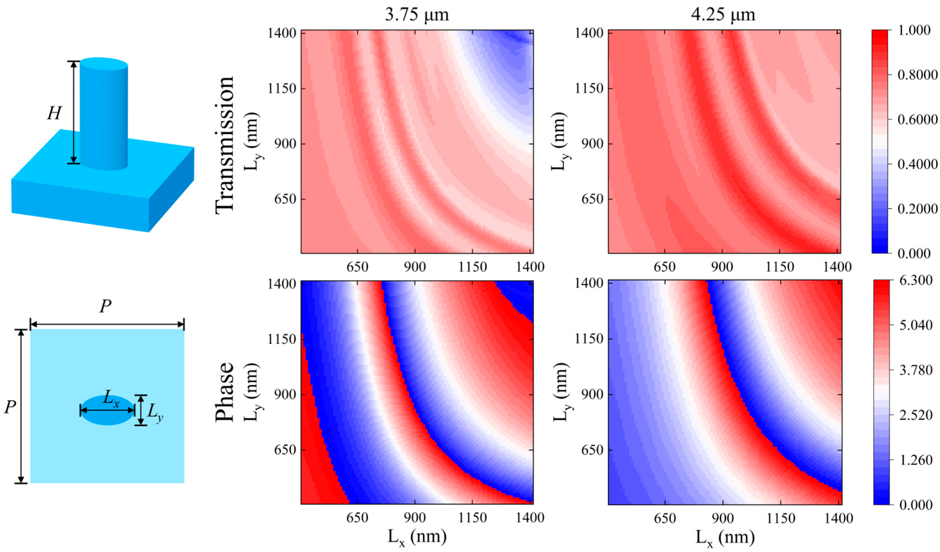
2.1. Construction of the Parameter Space for Infrared Metalens Elements

In this study, the achromatic design targets two discrete wavelengths, 3.75 μm and 4.25 μm, which were specifically chosen as they correspond to key points in the mid-wave infrared region, which is highly relevant for thermal imaging and other infrared applications. This approach allows for potential adaptation to other wavelength ranges by modifying the metasurface parameters.
Silicon is used as the substrate material for mid-wave infrared metalenses, with sub-wavelength elliptical nanopillars designed as the geometric form of the elements. The major and minor axes of the elliptical pillars serve as variable parameters for scanning. The pillar height (H) and period (P) are fixed at 4500 nm and 1650 nm, respectively, while the major and minor axes (Lx and Ly) range from 400 nm to 1400 nm. Using Ansys Lumerical FDTD 2023 R2.3, a detailed parameter scan was performed to establish the transmittance and phase spectra of these elements at the two working wavelengths, as shown in dimensions for x-polarized and y-polarized incidences, showing significant polarization dependence. This dependence facilitates the independent control of wavefront phases across polarization channels.
Figure 1 illustrates the parameter space related to x-polarization, specifically showing the variations of transmittance and phase spectra as functions of nanopillar dimensions (Lx = 2Rx and Ly = 2Ry). Considering the symmetric nature of the structure, for a y-polarized incidence, the characteristics of the spectra exhibit mirror symmetry in the parameter space relative to the diagonal line Lx = Ly. This parameter space demonstrates significant polarization dependence, which helps reduce interference between different polarization channels in the wavefront phase design of the light field, allowing for independent and effective control in each polarization channel.
The metalens designed in this thesis exhibits a focusing function under an x-polarized light incidence and generates focused vortex light under a y-polarized light incidence. The theoretical phase distribution formula is given as:
ϕ i x , y , λ = l i θ + 2 π λ f x 2 + y 2 + f 2 ,
where i = x or y, l x = 0, and l y 0 .

2.2. Amplitude Matching

The metalenses were designed individually for the working wavelengths of 3.75 μm and 4.25 μm. Under x-polarized and y-polarized incident light, the theoretical complex amplitude can be expressed as follows:
U k x , y , λ = A 0 e j ϕ k x , y , λ ,
Here, k = x or y, representing x-polarization or y-polarization. The complex amplitude of the i-th element under different polarization states can be expressed as:
U i k = A i k e j ϕ i k ,
One can sequentially traverse the complex amplitudes of all metalens elements at each position (x, y) on the metalens, according to the evaluation function:
D i f f i = k x , y A i k e j ϕ i k A 0 e j ϕ k x , y , λ ,
Based on the parameter space constructed in Figure 1, Ai for each element at the working wavelengths of 3.75 μm and 4.25 μm can be obtained, where i represents the i-th element. It is calculated that the average amplitude A 0 I at the working wavelength of 3.75 μm is 0.7907, and the average amplitude A 0 II at the working wavelength of 4.25 μm is 0.8680. In addition, a phase deviation analysis was conducted at both wavelengths to assess achromatic performance. The phase deviations at 3.75 μm and 4.25 μm were within the acceptable limits, indicating high phase consistency and effective achromatic focusing across both wavelengths.
One can select the i-th element with the smallest D i f f i to fill the corresponding position, until the elements fill the entire metalens area, ultimately constructing the entire metalens array.

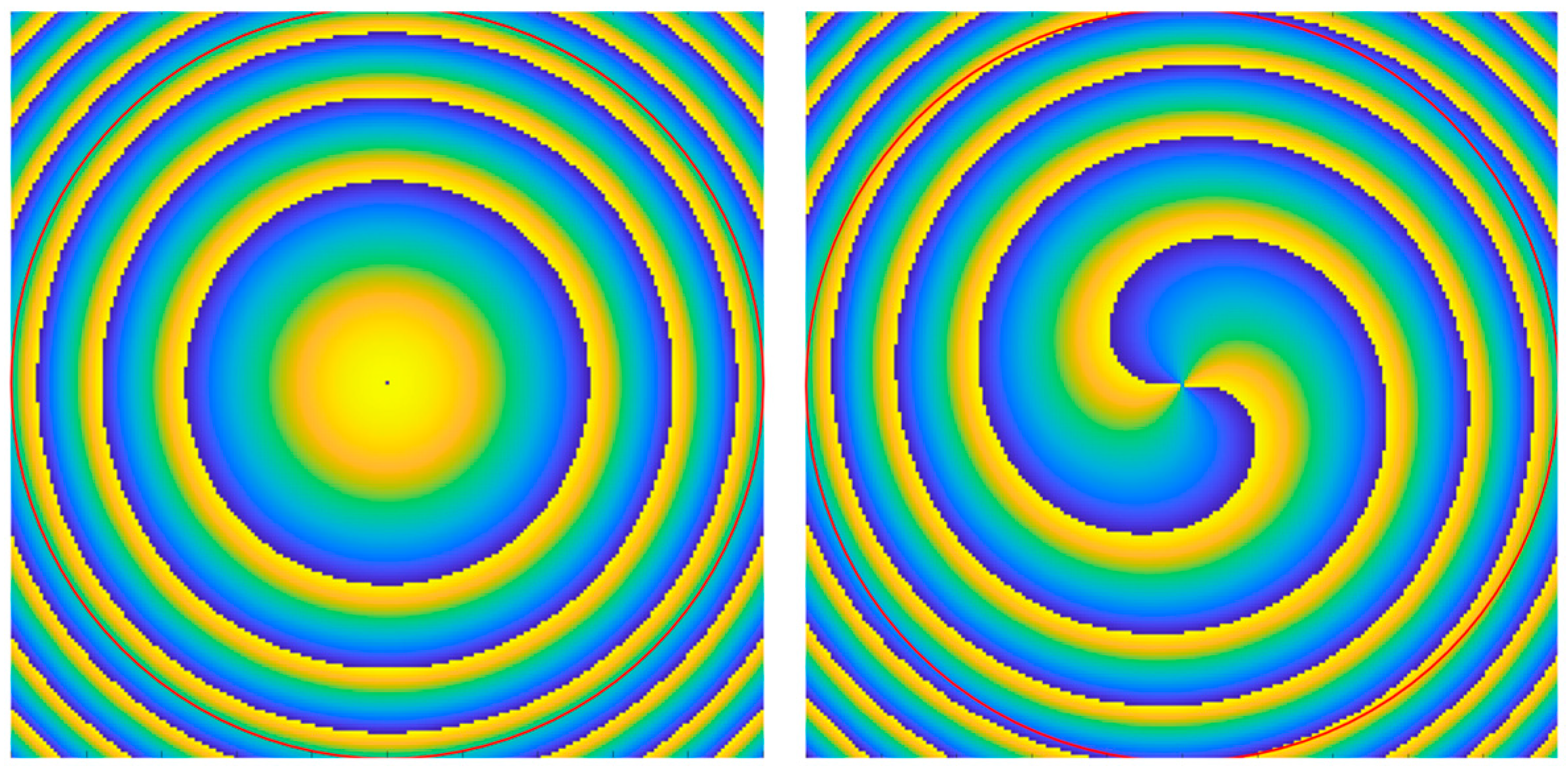
2.3. Analysis of Two Theoretical Phase Distributions

In multi-wavelength or broadband applications, chromatic aberration is a key challenge for metalens design [21,22]. To achieve broadband achromaticity, each metalens element must provide the required phase modulation at different wavelengths. However, the limited element types in the library often fall short as the aperture and element count increase [23,24]. This paper addresses this limitation through spatial multiplexing, which analyzes the compatibility of different phase distributions. By sparsifying and reconstructing metalens arrays for different wavelengths, the desired optical performance is achieved.
As an example, the phase distribution of a mid-wave infrared metalens with a 200 μm aperture is illustrated in Figure 2. The phase distributions for different polarization states are shown, with the circular red frame representing the edge of the 200 μm aperture mid-wave infrared metalens.
According to Equation (1), the corresponding phase gradient formulas for the focusing function and vortex beam generation are as follows:
Δ ϕ F = 2 π λ x i + y j x 2 + y 2 + f 2 ,
Δ ϕ V = l x 2 + y 2 y i + x j
The theoretical phase gradient describes the direction and rate of phase change. A complete function group on the phase plane defines the spatial region over which the phase completes one period. Figure 3a,b show the focusing phase distribution and its corresponding phase gradient, while Figure 3e,f show the vortex beam generation phase distribution and its phase gradient. For the focusing metalens, the complete function group is a radial row through the center, leading to sectoral sparsification of the array. For vortex beam generation, the group is a circular row around the center, leading to annular sparsification. Figure 3c,d illustrate sectoral sparsification and integrated spatial multiplexing, while Figure 3g,h show annular sparsification with multiplexing. The red and green elements represent the corresponding positions in the single-wavelength array.
When employing the complex function designs for focusing and vortex beam generation described in this paper, it was found that the focusing function, which ideally distributes its field at a point on the two-dimensional focal plane, imposes more relaxed requirements on the spatial distribution of the theoretical phase on the metalens. In contrast, the vortex beam generation function, with its ideal field distribution forming a ring on the two-dimensional focal plane and varying with different topological charges, demands stricter spatial integrity for the complete function group.
We tested three spatial multiplexing schemes for the polarization dual-function multiplexing metalens array with a 200 μm aperture in the mid-wave infrared range. The first scheme involves the complete function group of the focusing metalens, applying a 30° sectoral sparsification to each array before spatial multiplexing. The second scheme adopts a random arrangement, where elements are randomly selected and filled at each position from the corresponding elements of two different metalens arrays. The third scheme employs annular sparsification, which prioritizes the spatial integrity of the vortex beam generation function by maintaining a ring-like spatial distribution for the complete function group.
Testing these three spatial multiplexing methods using light with a wavelength of 4.25 μm, the intensity profiles were calculated using the FDTD method and are shown in Figure 4 and Figure 5b. The red and green elements, respectively, represent the elements from the corresponding single-wavelength metalens arrays. The comparison between these three schemes highlights the advantages of annular sparsification in preserving the spatial integrity required for vortex beam generation. This demonstrates its superiority over sectoral sparsification and random arrangement in effectively producing the desired optical functions.
The simulated results verified the previous analysis, showing that the realization of the focusing function is less affected by the different spatial multiplexing method, while the vortex beam generation function is significantly influenced by the spatial multiplexing method. Therefore, this paper selects the complete function group for the dual vortex beam function as the core functional group of the invention, as specifically shown in Figure 3g,h.
The proposed spatial multiplexing approach provides advantages over traditional single-wavelength designs by enabling dual-wavelength functionality with high phase fidelity. While polarization multiplexing has proven effective in previous studies, our method offers an efficient alternative for achieving multifunctional metalenses across discrete wavelengths.

3. Simulation

Following the aforementioned process, single-wavelength polarization dual-function multiplexing metalenses working at 3.75 μm and 4.25 μm wavelengths were constructed, as well as dual-wavelength polarization dual-function multiplexing metalenses operating at both wavelengths simultaneously. The aperture of the metalenses was set to achieve an F-number (F/#) of 3, which is critical for maintaining high focusing efficiency and ensuring practical applicability in large-aperture metalens designs. All results presented below were obtained through simulations using the FDTD method.

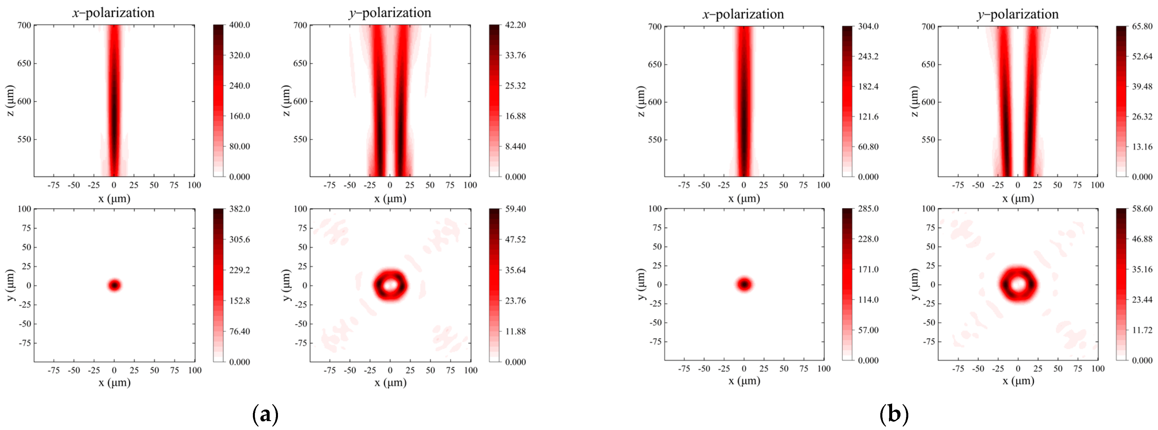
3.1. Single-Wavelength Polarization Dual-Function Multiplexing Metalens

The metalenses operating at single wavelengths (3.75 μm and 4.25 μm) were modeled separately. PML boundary conditions were chosen for all boundaries, and appropriate simulation parameters were set before starting the simulation. To shorten simulation time and improve efficiency, the initial simulation was performed using the mid-wave infrared metalens structure with a 200 μm aperture under 3.75 μm and 4.25 μm incident light. The simulated intensity profiles are shown in Figure 5.
From the simulated results, the designed single-wavelength polarization dual-function multiplexing metalens successfully achieved the expected target of F/# = 3. It realized the focusing function under x-polarized light incidence and generated vortex beams under y-polarized light incidence.

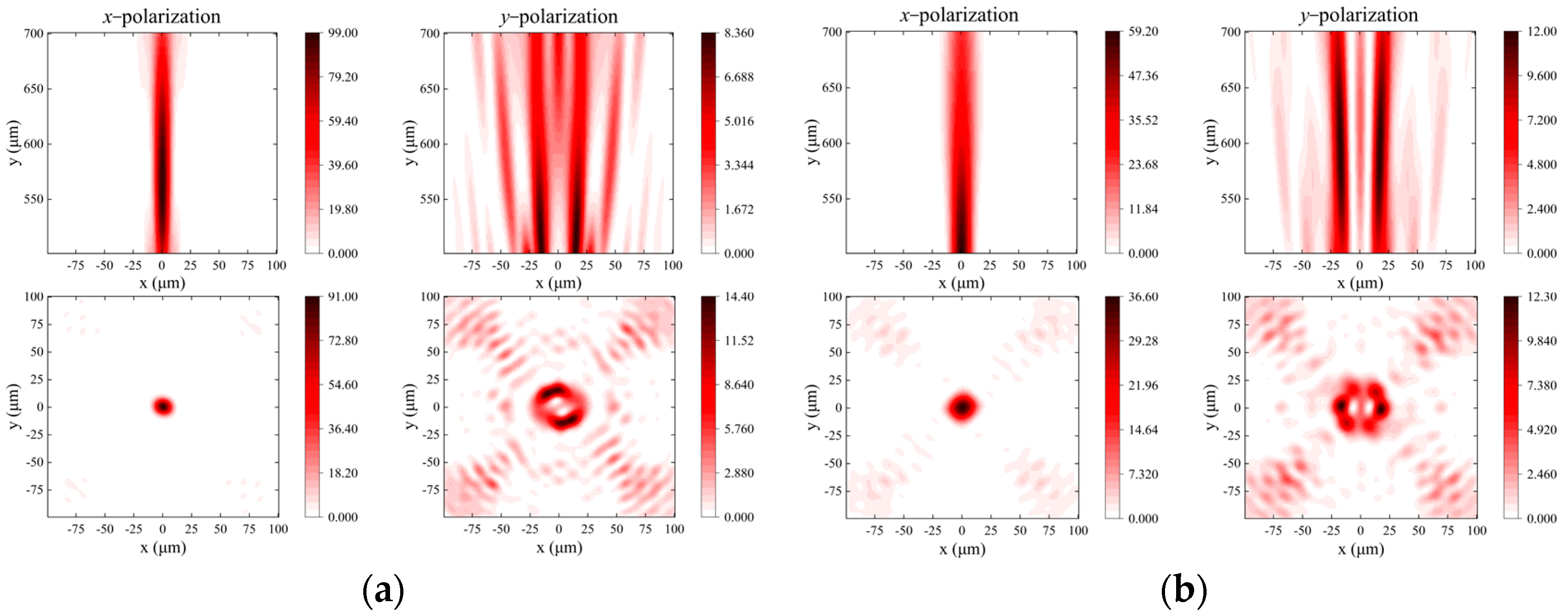
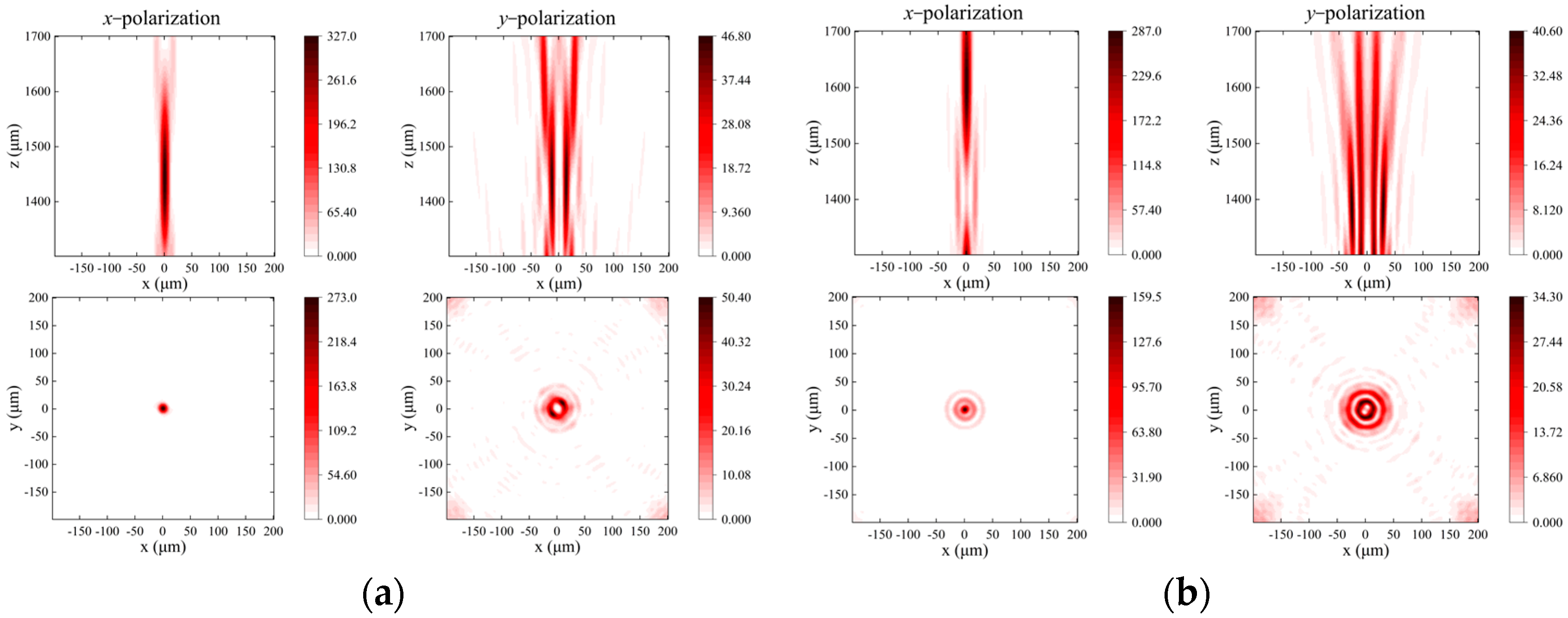
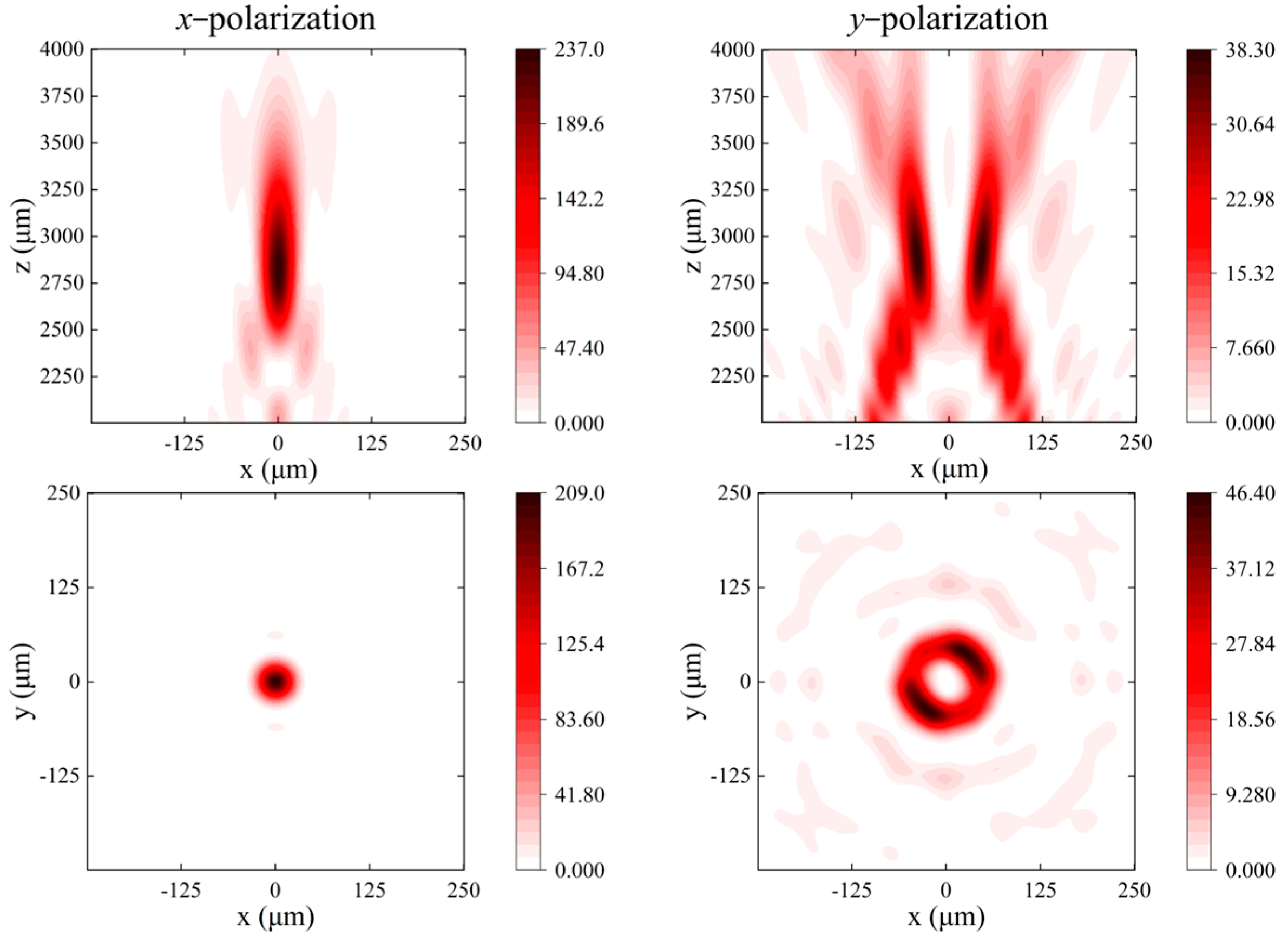
3.2. Dual-Wavelength Polarization Dual-Function Multiplexing Metalens
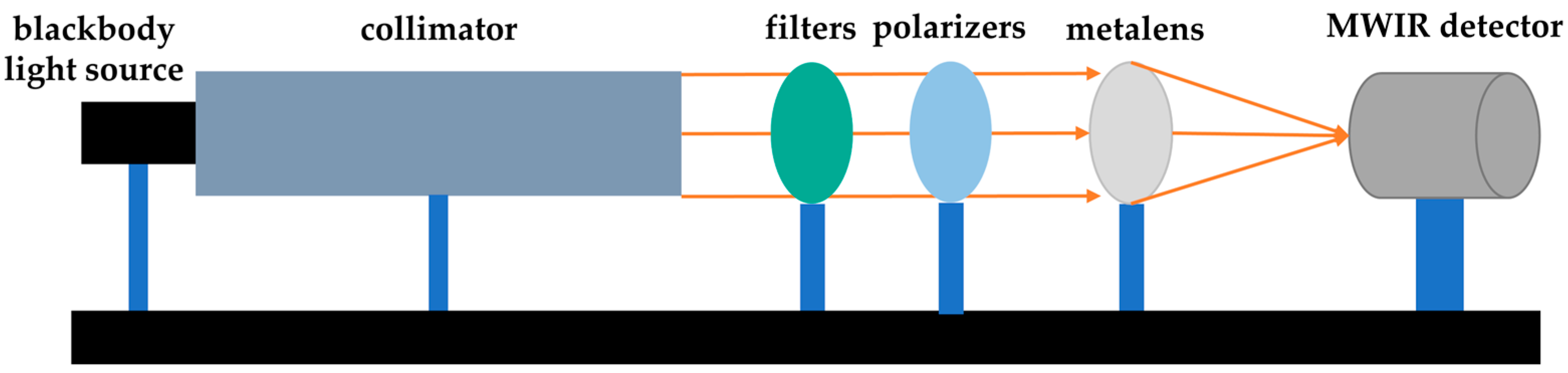
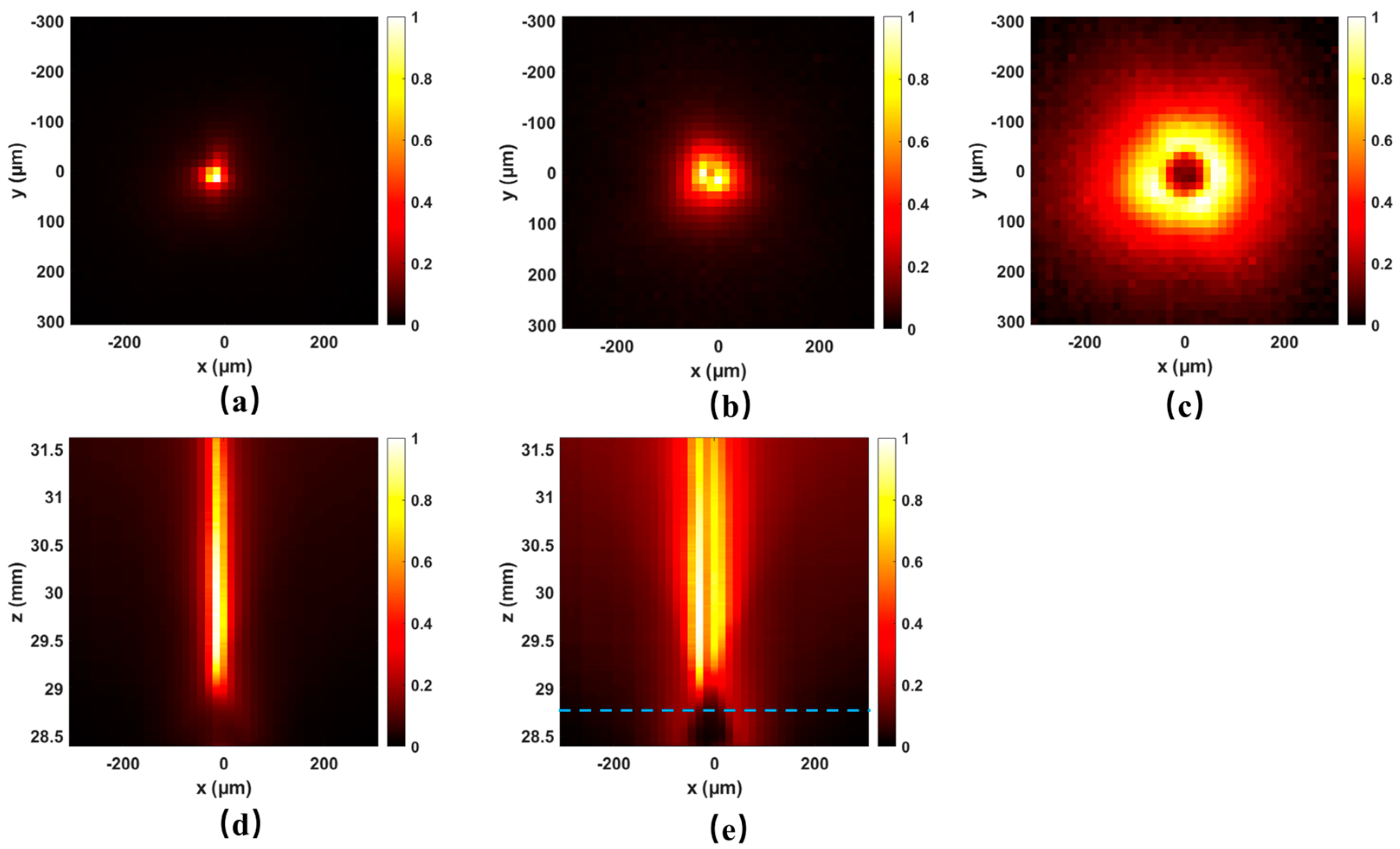
Through annular spatial multiplexing, the designed single-wavelength metalens arrays were integrated into one metalens, creating a dual-wavelength polarization dual-function multiplexing metalens that can achieve the desired functions at both working wavelengths.
First, the 200 μm aperture mid-wave infrared metalens was simulated. The simulated intensity profiles demonstrated its performance under 3.75 μm and 4.25 μm incident light, as shown in Figure 6.
The simulated results were consistent with our expectations, proving that the design scheme is effective at the same aperture scale. Due to limitations in computing power, we were unable to directly simulate centimeter-scale large-aperture metalenses. Therefore, we expanded the aperture to 500 μm and conducted the simulation again. The simulated intensity profiles under 3.75 μm and 4.25 μm incident light are shown in Figure 7.
From the results, it is evident that by using the spatial multiplexing method and the original theoretical phase distribution design, without the need for complex optimization algorithms to alter the theoretical phase distribution, the expanded aperture metalens retains its functionality. It continues to exhibit multi-wavelength polarization dual-function multiplexing capabilities, indicating that this design method can be extended to large apertures.
Using the same design approach, a 1 cm aperture dual-wavelength polarization dual-function multiplexing metalens array was developed. The layout design was carried out using a block drawing method, resulting in the final layout for the 1 cm large-aperture dual-wavelength polarization dual-function multiplexing metalens being ready for fabrication.

4. Characterization

The metalens was fabricated using standard photolithography and etching techniques, followed by cleaning to remove residual materials. The final structure was characterized, as shown in Figure 8, revealing a functional region diameter of 10.25 mm and a thickness of 0.19 mm.
The primary components of the metalens functionality testing system include a blackbody light source, an optical system (metalens, polarizers, filters), structural components (lens barrel, light shield, focal plane adjustment frame, etc.), an MWIR cooled infrared detector module, and an information processing and control unit. The infrared detector SCORPIO MW K508 (Lynred, Palaiseau, France) operates in the spectral range of 3.7 to 4.8 μm. These components work together to test and validate the performance of the metalens. The configuration of the testing system and the optical path are shown in Figure 9.
To validate the dual-wavelength functionality of the metalens, we employed the MWIR detector SCORPIO MW K508 for optical testing. First, without using any filters, we moved a one-dimensional adjustment stage back and forth to collect the two-dimensional light field distribution within a focal length adjustment range of 25 mm to 35 mm along the z-axis. The collected results were normalized, respectively, and are shown in Figure 10. Figure 10b shows the expected field distribution on the focal plane under a y-polarized light incidence. However, due to the phase singularity on the focal plane being smaller than the pixel size of the monitor (15 μm), the vortex light ring is not clearly visible. Instead, we collected the results at a position slightly away from the focal plane, as shown in Figure 10c, where the vortex pattern becomes clearly visible.
The light field distributions collected under x-polarized and y-polarized light incidences, after placing 3.75 μm and 4.25 μm filters in the optical path, are shown in Figure 11. To clearly demonstrate the generation of vortex light, the positions for data collection under a y-polarized light incidence were slightly away from the focal plane.
It can be observed that, under different polarized light incidences, the metalens exhibits significantly different functional expressions: focusing under an x-polarized light incidence and generating focused vortex beams (topological charge l = 2) under a y-polarized light incidence. The experimental results validate the accuracy of the simulations. It is important to compare the performance of the proposed metalens with other state-of-the-art dual-wavelength metalenses to highlight its advantages and innovations. Table 1 summarizes the working wavelength ranges, functionalities, and aperture sizes of the proposed metalens in comparison with recent works. This comparison underscores the unique capabilities of the proposed design, particularly its larger experimental aperture size.

5. Reapplication of the Design Method in Different Wavelength Ranges

To accommodate the varying requirements of different application scenarios across diverse wavelength ranges, this section demonstrates the versatility of the proposed design method by applying it to a different wavelength range. Using the same approach as in the mid-wave infrared design, we developed a metalens for the long-wave infrared range and verified its effectiveness through simulation. Germanium, which has excellent transmission properties in the long-wave infrared band, was used as the substrate material. Sub-wavelength elliptical nanopillars were employed as the research elements. The pillar height was fixed at 12 μm, and the period was set at 4700 nm, while the lengths of the major and minor axes of the elliptical pillars varied between 1 μm and 4 μm. Using FDTD algorithm software, detailed parameter scans of these metalens elements were performed to explore the mapping relationship between the two geometric degrees of freedom and the transmittance and phase modulation. This ultimately generated a parameter space containing the phase spectra and transmittance spectra information of the elements. In the numerical simulations, perfect matching layer (PML) boundary conditions were used for the light propagation direction, while periodic boundary conditions were applied in the x and y directions. The incident light was introduced in x-polarized and y-polarized forms, with wavelengths of 10 μm and 12 μm, respectively.
Figure 12 shows the data related to x-polarization from the element database, detailing how the transmittance and phase spectra vary with changes in the nanopillar dimensions (Lx = 2Rx and Ly = 2Ry). Following a similar procedure as described for the wavelengths of 3.75 μm and 4.25 μm, the transmittance values at 10 μm and 12 μm were obtained. The average amplitudes at 10 μm and 12 μm are 0.6077 and 0.7725, respectively.
Using these values, we constructed the metalens arrays and performed numerical simulations for apertures of 1 mm, with the exemplary results for the 1 mm aperture at 12 μm shown in Figure 13. The results indicate that by using the spatial multiplexing method to achieve dual-wavelength functionality, and employing the original theoretical phase distribution for the design without the need for complex optimization algorithms to alter the theoretical phase distribution, the same effectiveness is achieved in the long-wave infrared band. This verifies the versatility of the design scheme across different operating wavelength bands.

6. Conclusions

In this study, we have demonstrated the successful design and fabrication of dual-wavelength polarization multifunction metalenses utilizing a novel spatial multiplexing approach. This method effectively addresses the challenges of achieving large apertures while maintaining high optical performance across multiple wavelengths. Through both simulations and experimental validation, we confirmed that the metalenses designed in this work are capable of polarization dual-function multiplexing in the mid-wave infrared range. The application of spatial multiplexing has significantly expanded the potential of metalenses for high-performance optical systems, providing new pathways for compact, efficient, and multifunctional optoelectronic devices. These findings offer a promising foundation for future advancements in metasurface-based technologies, with potential applications in imaging, sensing, and communication systems. Future work will focus on extending this design approach to other wavelength ranges and optimizing the fabrication process for large-scale production. Additionally, integrating these metalenses into practical optical systems will further explore their full potential in real-world applications.

Author Contributions

Conceptualization, X.S. and W.L.; methodology, X.S., W.L. and Y.Z.; validation, X.S. and H.H.; formal analysis, X.S. and W.L.; investigation, Y.L., X.S. and J.G.; data curation, X.S.; writing—original draft preparation, X.S.; writing—review and editing, X.S. and W.L.; supervision, W.L.; project administration, W.L.; funding acquisition, W.L. All authors have read and agreed to the published version of the manuscript.

Funding

This research was funded by the National Natural Science Foundation of China (Grants 62075232 and 92163134), the Autonomous Deployment Project of State Key Laboratory of Materials for Integrated Circuits (SKLJC-Z2024-B08), the CAS Project for Young Scientists in Basic Research (YSBR-081), the Shanghai Sailing Program (22YF1456600), and the National Natural Science Foundation of China(No. 62305366).

Institutional Review Board Statement

Not applicable.

Informed Consent Statement

Not applicable.

Data Availability Statement

The data are contained within the article.

Conflicts of Interest

The authors declare no conflicts of interest.

References

  1. Sun, S.; Yang, K.-Y.; Wang, C.-M.; Juan, T.-K.; Chen, W.T.; Liao, C.Y.; He, Q.; Xiao, S.; Kung, W.-T.; Guo, G.-Y.; et al. High-Efficiency Broadband Anomalous Reflection by Gradient Meta-Surfaces. Nano Lett. 2012, 12, 6223–6229. [Google Scholar] [CrossRef]
  2. Arbabi, A.; Arbabi, E.; Kamali, S.M.; Horie, Y.; Han, S.; Faraon, A. Miniature optical planar camera based on a wide-angle metasurface doublet corrected for monochromatic aberrations. Nat. Commun. 2016, 7, 13682. [Google Scholar] [CrossRef] [PubMed]
  3. Li, X.; Xiao, S.; Cai, B.; He, Q.; Cui, T.J.; Zhou, L. Flat metasurfaces to focus electromagnetic waves in reflection geometry. Opt. Lett. 2012, 37, 4940. [Google Scholar] [CrossRef]
  4. Fang, N.; Lee, H.; Sun, C.; Zhang, X. Sub-diffraction-limited optical imaging with a silver superlens. Science 2005, 308, 534–537. [Google Scholar] [CrossRef] [PubMed]
  5. Kauranen, M.; Zayats, A.V. Nonlinear plasmonics. Nat. Photonics 2012, 6, 737–748. [Google Scholar] [CrossRef]
  6. Shalaev, V.M. Optical negative-index metamaterials. Nat. Photonics 2007, 1, 41–48. [Google Scholar] [CrossRef]
  7. Chen, C.; Song, W.; Chen, J.-W.; Wang, J.-H.; Chen, Y.H.; Xu, B.; Chen, M.-K.; Li, H.; Fang, B.; Chen, J.; et al. Spectral tomographic imaging with aplanatic metalens. Light Sci. Appl. 2019, 8, 99. [Google Scholar] [CrossRef] [PubMed]
  8. Zhang, S.; Soibel, A.; Keo, S.A.; Wilson, D.; Rafol, S.B.; Ting, D.Z.; She, A.; Gunapala, S.D.; Capasso, F. Solid-immersion metalenses for infrared focal plane arrays. Appl. Phys. Lett. 2018, 113, 111104. [Google Scholar] [CrossRef]
  9. Khorasaninejad, M.; Capasso, F. Metalenses: Versatile multifunctional photonic components. Science 2017, 358, eaam8100. [Google Scholar] [CrossRef]
  10. Zuo, H.; Choi, D.Y.; Gai, X.; Ma, P.; Xu, L.; Neshev, D.N.; Zhang, B.; Luther-Davies, B. High-Efficiency All-Dielectric Metalenses for Mid-Infrared Imaging. Adv. Opt. Mater. 2017, 5, 1700585. [Google Scholar] [CrossRef]
  11. Decker, M.; Chen, W.T.; Nobis, T.; Zhu, A.Y.; Khorasaninejad, M.; Bharwani, Z.; Capasso, F.; Petschulat, J. Imaging Performance of Polarization-Insensitive Metalenses. ACS Photonics 2019, 6, 1493–1499. [Google Scholar] [CrossRef]
  12. Guo, L.; Hu, Z.; Wan, R.; Long, L.; Li, T.; Yan, J.; Lin, Y.; Zhang, L.; Zhu, W.; Wang, L. Design of aluminum nitride metalens for broadband ultraviolet incidence routing. Nanophotonics 2018, 8, 171–180. [Google Scholar] [CrossRef]
  13. Zhao, M.; Chen, M.K.; Zhuang, Z.-P.; Zhang, Y.; Chen, A.; Chen, Q.; Liu, W.; Wang, J.; Chen, Z.-M.; Wang, B.; et al. Phase characterisation of metalenses. Light. Sci. Appl. 2021, 10, 52. [Google Scholar] [CrossRef] [PubMed]
  14. Fan, Y.; Yao, J.; Tsai, D.P. Advance of large-area achromatic flat lenses. Light Sci. Appl. 2023, 12, 51. [Google Scholar] [CrossRef] [PubMed]
  15. Yuan, Y.; Yan, Z.; Zhang, P.; Chang, Z.; Peng, F.; Chen, R.; Yang, Z.; Chen, S.; Zhao, Q.; Huang, X. A Broadband Achromatic Dielectric Planar Metalens in Mid-IR Range. Photonic Sens. 2023, 13, 230126. [Google Scholar] [CrossRef]
  16. Baek, S.; Kim, J.; Kim, Y.; Seok Cho, W.; Badloe, T.; Moon, S.-W.; Rho, J.; Lee, J.-L. High numerical aperture RGB achromatic metalens in the visible. Photonics Res. 2022, 10, B30. [Google Scholar] [CrossRef]
  17. He, M.; Wu, J.; Chen, H.; Wang, H.; Wu, X.; Feng, Q.; Wu, Q.; Wu, X.; Liu, H.; Li, Q.; et al. High efficiency independent modulation at dual-wavelength based on Pancharatnam–Berry and propagation phases. J. Opt. Soc. Am. B 2024, 41, 1076–1083. [Google Scholar] [CrossRef]
  18. Xu, F.; Liu, P.; Chen, W.; Li, M.; Chen, Y. Polarization-modulated dual-wavelength metalens to overcome the diffraction limit. Opt. Commun. 2024, 572, 130975. [Google Scholar] [CrossRef]
  19. Zhu, W.; Fan, Y.; Yang, R.; Geng, G.; Fu, Q.; Gu, C.; Li, J.; Zhang, F. Polarization-Multiplexed Silicon Metasurfaces for Multi-Channel Visible Light Modulation. Adv. Funct. Mater. 2022, 32, 2200013. [Google Scholar] [CrossRef]
  20. Fan, Q.; Liu, M.; Zhang, C.; Zhu, W.; Wang, Y.; Lin, P.; Yan, F.; Chen, L.; Lezec, H.J.; Lu, Y.; et al. Independent Amplitude Control of Arbitrary Orthogonal States of Polarization via Dielectric Metasurfaces. Phys. Rev. Lett. 2020, 125, 267402. [Google Scholar] [CrossRef]
  21. Ali, F.; Aksu, S. A hybrid broadband metalens operating at ultraviolet frequencies. Sci. Rep. 2021, 11, 2303. [Google Scholar] [CrossRef]
  22. Wang, Y.; Chen, Q.; Yang, W.; Ji, Z.; Jin, L.; Ma, X.; Song, Q.; Boltasseva, A.; Han, J.; Shalaev, V.M.; et al. High-efficiency broadband achromatic metalens for near-IR biological imaging window. Nat. Commun. 2021, 12, 5560. [Google Scholar] [CrossRef] [PubMed]
  23. Khorasaninejad, M.; Shi, Z.; Zhu, A.Y.; Chen, W.T.; Sanjeev, V.; Zaidi, A.; Capasso, F. Achromatic Metalens over 60 nm Bandwidth in the Visible and Metalens with Reverse Chromatic Dispersion. Nano Lett. 2017, 17, 1819–1824. [Google Scholar] [CrossRef] [PubMed]
  24. Vogliardi, A.; Ruffato, G.; Dal Zilio, S.; Bonaldo, D.; Romanato, F. Dual-functional metalenses for the polarization-controlled generation of focalized vector beams in the telecom infrared. Sci. Rep. 2023, 13, 10327. [Google Scholar] [CrossRef] [PubMed]
  25. Wang, S.; Wu, P.C.; Su, V.-C.; Lai, Y.-C.; Hung Chu, C.; Chen, J.-W.; Lu, S.-H.; Chen, J.; Xu, B.; Kuan, C.-H.; et al. Broadband achromatic optical metasurface devices. Nat. Commun. 2017, 8, 187. [Google Scholar] [CrossRef] [PubMed]
  26. Ou, K.; Yu, F.; Li, G.; Wang, W.; Miroshnichenko, A.E.; Huang, L.; Wang, P.; Li, T.; Li, Z.; Chen, X.; et al. Mid-infrared polarization-controlled broadband achromatic metadevice. Sci. Adv. 2020, 6, eabc0711. [Google Scholar] [CrossRef] [PubMed]
  27. Ou, K.; Yu, F.; Li, G.; Wang, W.; Chen, J.; Miroshnichenko, A.; Huang, L.; Li, T.; Li, Z.; Chen, X.; et al. Broadband Achromatic Metalens in Mid-Wavelength Infrared. Laser Photonics Rev. 2021, 15, 2100020. [Google Scholar] [CrossRef]
Figure 1. Schematic of all silicon-based elliptical column meta-atoms and meta-atoms’ parameter space.
Photonics 12 00061 g001
Figure 2. Phase distribution schematic of focus (left) and vortex light generation (right).
Photonics 12 00061 g002
Figure 3. (a) Phase distribution schematic of focusing phase. (b) Schematic of focusing phase gradient vector. (c) Schematic of fan-shaped sparsity. (d) Schematic of sector spatial multiplexing. (e) Phase distribution schematic of vortex light generation (l = 2). (f) Schematic of vortex light generation (l = 2) phase gradient vector. (g) Schematic of ring sparsity. (h) Schematic of ring spatial multiplexing.
Photonics 12 00061 g003
Figure 4. Schematic and simulated intensity profiles of sector space multiplexing and random space multiplexing.
Photonics 12 00061 g004
Figure 5. Simulated intensity profiles of the 200 μm MWIR single-wavelength metalens under 3.75 μm (a) and 4.25 μm (b) incident light.
Photonics 12 00061 g005
Figure 6. Simulated intensity profiles of the 200 μm dual-wavelength metalens under 3.75 μm (a) and 4.25 μm (b) incident light.
Photonics 12 00061 g006
Figure 7. Simulated intensity profiles of the 500 μm dual-wavelength metalens under 3.75 μm (a) and 4.25 μm (b) incident light.
Photonics 12 00061 g007
Figure 8. (a) Image of MWIR dual-wavelength polarization bifunctional multiplexed infrared metalens. (b) Scanning electron microscope (SEM) images of MWIR dual-wavelength polarization bifunctional multiplexed infrared metalens.
Photonics 12 00061 g008
Figure 9. Test optical path diagram.
Photonics 12 00061 g009
Figure 10. Light field distribution results (a) at the focal plane with x-polarized light incidence, (b) at the focal plane with y-polarized light incidence, (c) slightly away from the focal plane with y-polarized light incidence, and (d,e) with longitudinal directions with x-polarized and y- polarized light incidence.
Photonics 12 00061 g010
Figure 11. Light field distribution results (a,c) at the focal plane with x-polarized light incidence at wavelengths of 3.75 μm and 4.25 μm and (b,d) slightly away from the focal plane with y-polarized light incidence at wavelengths of 3.75 μm and 4.25 μm.
Photonics 12 00061 g011
Figure 12. Schematic of germanium-based elliptical column meta-atoms’ parameter space.
Photonics 12 00061 g012
Figure 13. Simulated intensity profiles of the 1 mm LWIR dual-wavelength metalens (12 μm).
Photonics 12 00061 g013
Table 1. Performance comparison.
Working WavelengthFunctionAperture SizeFocusing Efficiency
Literature [19]0.4–0.7 μmPolarization Function Multiplexing324 μm
Literature [25]1.2–1.68 μmAchromatic Focusing55.55 μm8.4%, 12.44%, and 8.56%
Literature [26]3.5–5 μmPolarization Function Multiplexing200 μm
Literature [27]3.5–5 μmAchromatic Focusing, Vortex Beam Generation200 μm45%
Literature [15]4–5 μmAchromatic Focusing100 μm51.6%
This work3.7–4.8 μmPolarization Function Multiplexing10,000 μm43.77%
Disclaimer/Publisher’s Note: The statements, opinions and data contained in all publications are solely those of the individual author(s) and contributor(s) and not of MDPI and/or the editor(s). MDPI and/or the editor(s) disclaim responsibility for any injury to people or property resulting from any ideas, methods, instructions or products referred to in the content.

