Communication

Research on Pt-Based Film Negative Photoconductivity Photothermal Detector Under Different Wavelength Laser Irradiation

1
Center of Intelligent Opto-Electric Sensors, Tianjin Jinhang Technical Physics Institute, Tianjin 300308, China
2
School of Mechanical Engineering, Jiangsu University, Zhenjiang 212013, China
3
School of Precision Instruments and Opto-Electronics Engineering, Tianjin University, Tianjin 300072, China
4
School of Electronic and Information Engineering, Hebei University of Technology, Tianjin 300401, China
*
Authors to whom correspondence should be addressed.
Photonics 2025, 12(1), 6; https://doi.org/10.3390/photonics12010006
Submission received: 10 November 2024 / Revised: 16 December 2024 / Accepted: 23 December 2024 / Published: 24 December 2024

Abstract

:
Platinum (Pt) is a rare and precious metal element with numerous unique properties. These properties have led to the widespread use of Pt in electronic components, thermocouples, and high-temperature devices. In this study, we present the bolometric effect of single-metal Pt-based negative photoconductivity (NPC) devices under the laser irradiation of 375 nm, 532 nm, and 808 nm. Under the condition of applying 0.5 V voltage, the responsivity (R) of the Pt photothermal detector (Pt-PTD) under 375 nm laser irradiation was 69.14 mA/W, and the specific detectivity (D*) was 5.38 × 10⁷ Jones; the R of the Pt-PTD under 532 nm laser irradiation was 59.46 mA/W, and the D* was 4.61 × 10⁷ Jones; the R of the Pt-PTD under 808 nm laser irradiation was 37.88 mA/W, and the D* was 2.95 × 10⁷ Jones. Additionally, a single-site scanning imaging system based on a Pt-PTD was designed to test the capability of the device. This study provides a strategy for the development of thermal measurement detectors based on Pt materials.

1. Introduction

A photoelectric device is a device that can convert optical signals into electrical signals; according to different light response mechanisms, photoelectric devices can be divided into two categories: PTD and photon detectors [1,2,3,4,5,6]. The principle of the PTD is to convert the light radiation energy absorbed by the material into the thermal motion energy of the lattice [7], triggering different mechanisms, changing the physical properties, and then measuring and converting it into electrical signals [8,9]. In PTDs based on photothermal conversion, electrons excited by light return to the ground state through a non-radiative transition, releasing the absorbed light energy mainly in the form of heat [10]. The spectral response range of the photon detector is limited by the band gap of the active material [11], while the PTD can respond to a wider spectrum, especially in the infrared region, where the photothermal effect is more obvious [10]. Detectors based on the bolometric effect have a wide range of infrared detection, thermal imaging, and temperature measurement. They provide important technical support for industrial, military, and medical applications [12,13,14]. Examples include photothermal therapy [15], light energy harvesting in photocatalysis [16], thermo-optical data storage, and optoelectronic devices [17,18]. Although the photothermal effect of materials and structures has received much attention, it needs further study in the field of light detection. In addition, the performance parameters of PTD, such as response time and R, have been questioned due to a lack of sufficient evidence [11].
Pt is a rare and precious metal with many unique properties such as corrosion resistance, high melting point, high density, and excellent catalytic performance [19]. Pt has good thermal conductivity, which allows heat to transfer quickly. Pt is therefore widely used in electronic components, thermocouples, and other high-temperature applications [20]. The research of Pt in the field of detection mainly focuses on the enhancement of the performance of the detector by Pt nanoparticles (NPs). Tian and colleagues fabricated a series of ultraviolet photodetectors with Pt NPs on MgZnO thin films, which improved the dark current of the device and enhanced the performance of visible-blind photodetectors [21]. Pei et al. reported a metal–semiconductor–metal ultraviolet photodetector based on a ZnO film/Pt NPs/ZnO film composite structure. By embedding Pt NPs in the ZnO film and varying the embedding depth of the Pt NPs, they achieved a controllable enhancement range of the sensitivity of the ZnO ultraviolet photodetector [22]. Zeng et al. reported that decorating vanadium pentoxide (V2O5) nanobelts with Pt NPs can significantly improve the performance of Schottky-contacted photodetectors. After Pt NPs modification, the photocurrent of V2O5 nanobelts increased by more than two orders of magnitude, while the photo-response speed improved by at least three orders of magnitude [23]. However, there are few reports on detectors based on metal Pt thin films.
In this study, a single-metal Pt-PTD was fabricated to take advantage of the excellent thermal conductivity of Pt. The NPC performance of Pt-PTD was tested in the range of ultraviolet to near-infrared light, and the bolometric effect of PT-PTD was observed under three different laser wavelengths. The R of the devices under 375 nm, 532 nm, and 808 nm laser irradiation is measured at 69.14 mA/W, 59.46 mA/W, and 37.88 mA/W, respectively, while their D* is calculated as 5.38 × 10⁷ Jones, 4.61 × 10⁷ Jones, and 2.95 × 10⁷ Jones, respectively. This study provides valuable insights into the bolometric effects of Pt in the ultraviolet to near-infrared light range and offers strategies for developing and applying new Pt-based optoelectronic devices in practical applications.

2. Experimental Section

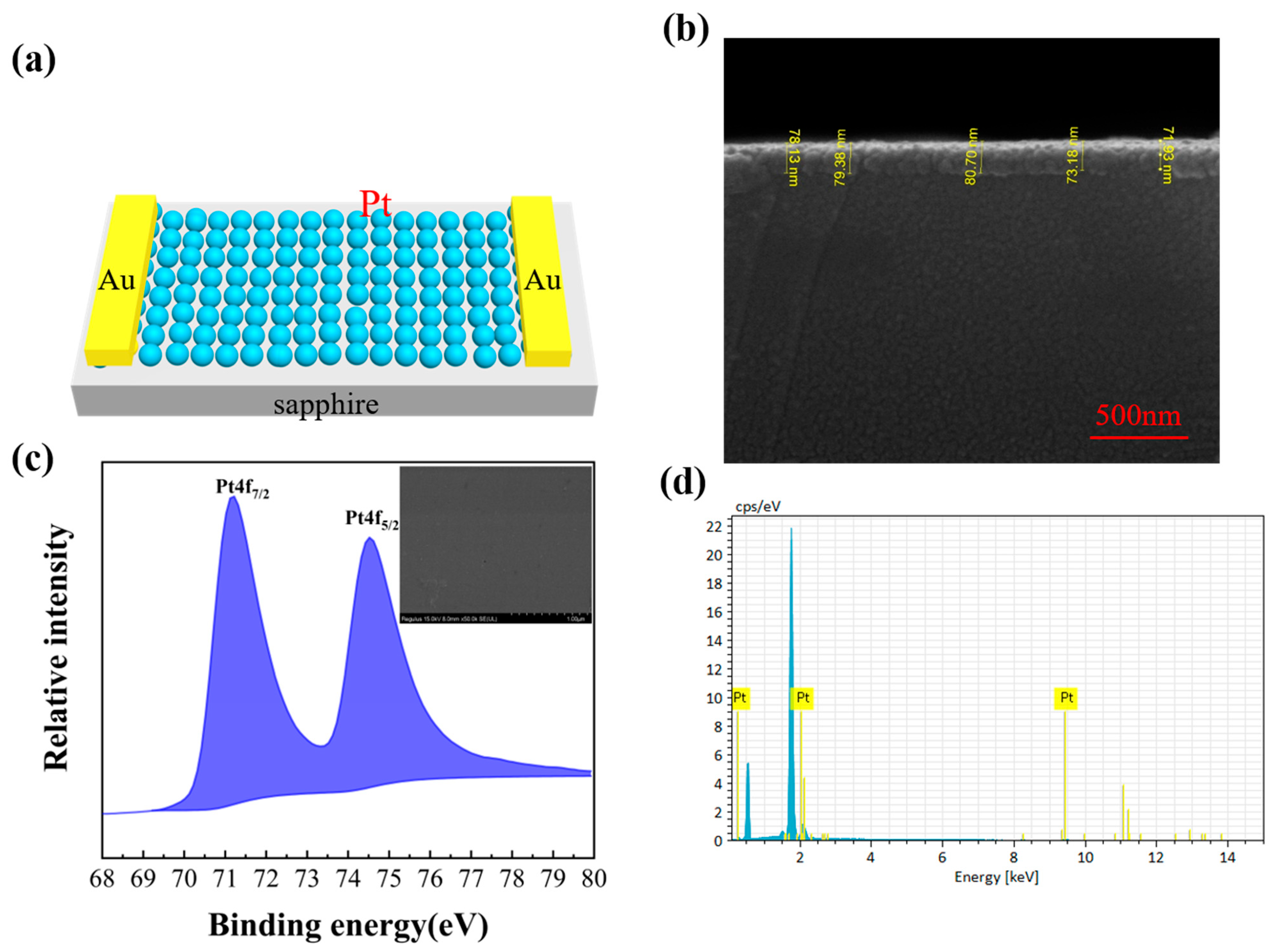
2.1. Device Preparation

First, clean the sapphire substrate with an ultrasonic cleaner, followed by acetone, deionized water, and ethanol; clean each for 5 min, and then dry under nitrogen protection. Put the clean sapphire substrate into the sample room, and ensure that the water, air, and power supply are normal. Turn on the cooling water and fill the sample room with nitrogen. After the vacuum is pumped to 1 Pa by mechanical pump, argon gas is put in and the pressure of argon is adjusted between 5 and 10 Pa. Press the RF source switch and the filament switch on the RF power supply and preheat for about 5 min. After preheating, deposit the Pt film on the sapphire surface by RF magnetron sputtering. Finally, 10 nm chromium and 300 nm gold are grown on Pt thin films by vacuum thermal evaporation to prepare PTDs.

2.2. Material Characterization and Device Measurement

The surface of Pt films was characterized by field emission scanning electron microscopy (FE-SEM) (Quanta FEG 250, FEI, Hillsboro, ON, USA). An analysis of Pt thin-film materials was performed using X-ray photoelectron spectroscopy (XPS) (ESCALAB 250Xi, Waltham, MA, USA) and energy dispersive X-ray spectroscopy (EDS) (Ultim Max, Abingdon, UK).
Two Au electrodes are connected to the two output ports of the Keithley 2400 as a source and drained to detect the channel current of the device under the application of an applied drain-source voltage. The photoelectric tests were performed under 375 nm, 532 nm, and 808 nm illumination.

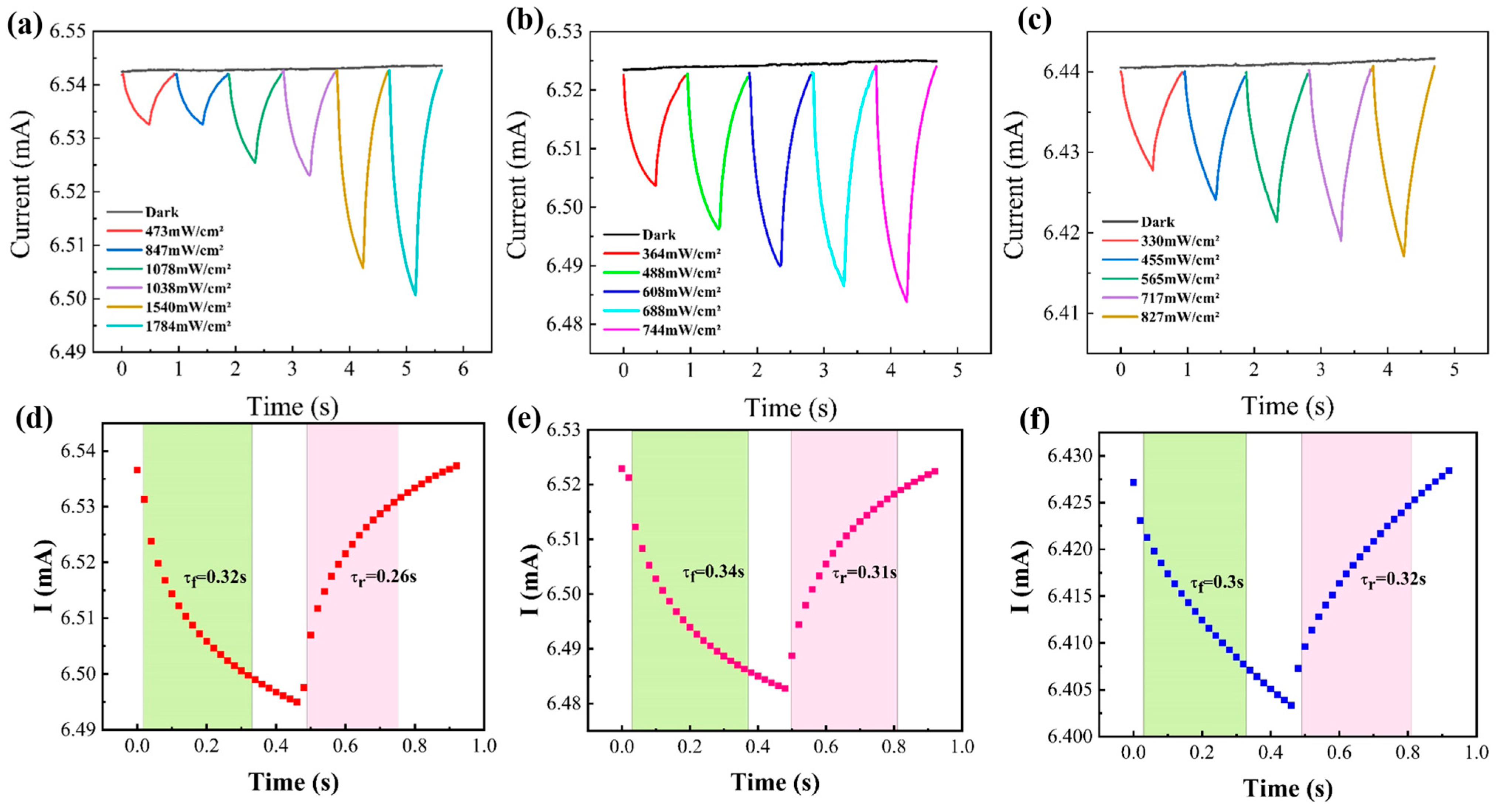
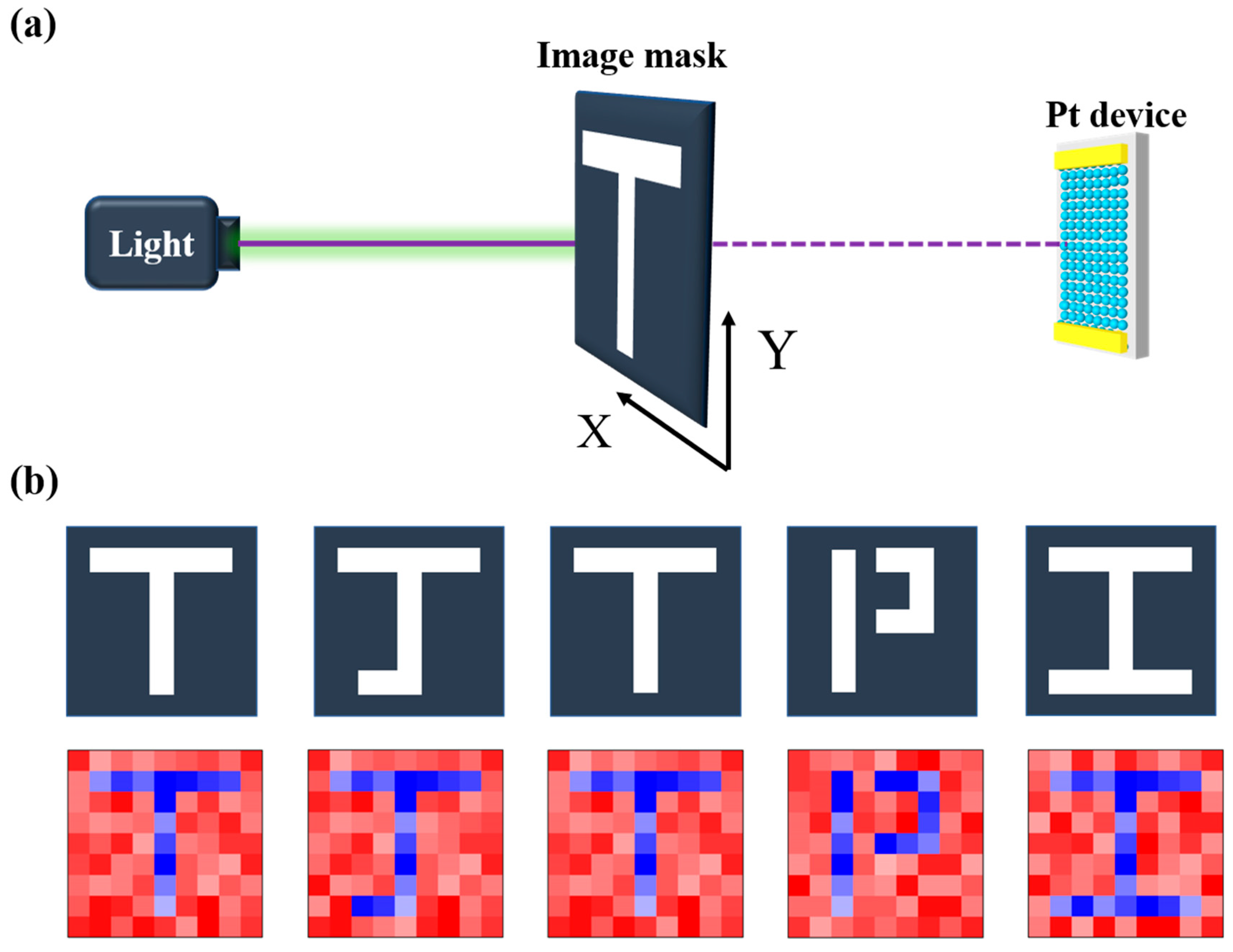
3. Discussion and Results

Figure 1a shows the schematic diagram of the Pt-PTD, which utilizes sapphire as the substrate with a Pt thin film deposited on the sapphire surface and Au electrodes at both ends. The cross-section morphology of Pt-PTD under a 500 nm scanning scale is depicted in Figure 1b, revealing a thickness of approximately 78 nm for the Pt film and 1 mm for the sapphire. The XPS of the Pt film (the inset is the SEM image of the Pt surface) is presented in Figure 1c, and it can be seen from the inset that the Pt film is uniformly distributed over the surface of the substrate, where peaks at 72.6 eV and 75.98 eV correspond to the Pt 4f7/2 and Pt 4f5/2 orbitals, respectively. As shown in Figure 1d, the EDS analysis of the thin film confirms that the thin-film material on the substrate is Pt.
The I-V curves of Pt-TPD at 375 nm, 532 nm, and 808 nm are depicted in Figure 2a–c. The channel current (IDS) is modulated by the voltage (VDS) and optical power, and the device operates as a PTD. It can be observed from the graphs that the IDS of Pt devices increases linearly with voltage at three different wavelengths. Additionally, as the laser power density increases, the IDS exhibits a decreasing trend, known as negative response. A quantitative evaluation of the device performance was conducted, and the R and D* of the device were calculated separately to analyze the performance of Pt-PTD. R is defined as the ratio of the current or the voltage of a PD to the incident light power [24]. It can be calculated using Equation (1).
R = Δ I D S P = I i l l I d a r k E e × S
where I i l l is the currents of the Pt-PTD under illumination; I d a r k is the currents of the Pt-PTD in the dark; E e is the light irradiance of the light source; S is the effective area of the channel, which is the product of the width and length of the device channel (the width of the device channel is 2.5 mm and the length is 50 µm). The D* is the ratio of the generation rate to the recombination rate of carriers which reflects the ability of the device to detect weak light signals [25], and can be expressed as follows:
D * = R W L 2 e I d a r k
where W represents instrument channel width and L represents instrument channel length. We have obtained the R and D* of the Pt-PTD under the irradiation of 375 nm, 532 nm, and 808 nm lasers (the voltage of the device is 0.5 V), as shown in Figure 2d–f. The R and D* of the Pt-PTD decreased with the increase in the irradiation density. The deterioration of the response time of Pt-PTD under high-power laser irradiation is related to various factors such as thermal accumulation, thermal stress, and changes in material properties. When irradiated with a 375 nm laser, the device has an R of 69.14 mA/W and a D* of 5.38 × 10⁷ Jones. With a 532 nm laser, the device’s R is 59.46 mA/W and the D* is 4.61 × 10⁷ Jones. Under the influence of an 808 nm laser, the device exhibits an R of 37.88 mA/W and a D* of 2.95 × 10⁷ Jones. From comparing the three data sets, it is evident that the R and D* of the Pt-PTD under 375 nm laser irradiation are higher than those under 532 nm and 808 nm laser irradiation. This suggests that the NPC response of the device is more pronounced in the 375 nm band compared to the 532 nm and 808 nm bands.
The transient response time, as an important device parameter, reflects the ability of the PTD to rapidly track the change in optical signals. The fast time response is very important for high-speed optical communication and fast photo-switch applications. Figure 3a–c show the variation in the IDS flowing through the Pt-PTD over time under 375 nm, 532 nm, and 808 nm lasers. We characterize the response time of Pt-PTD to lasers of different wavelengths using periodic optical switching devices. Upon observation, the Pt-PTD was found to have good periodicity and persistence. The graph shows that the current gradually decreases as the optical path is switched on and gradually increases as the optical path is switched off. When no laser is applied, the optical response range of the device remains largely unchanged. The IDS gradually decreases as the laser power increases, which confirms the presence of an NPC response in all three bands. Figure 3d–f shows the response time of a single optical switch in the Pt-PTD when exposed to 375 nm, 532 nm, and 808 nm laser radiation, respectively. The rise time ( τ r ) is defined as the time taken for the current to rise from 10% to 90% of the maximum current. The fall time ( τ f ) is defined as the time taken for the current to decay from 90% to 10% of the maximum current [26]. The rise and fall times of the Pt-PTD under 375 nm, 532 nm, and 808 nm laser irradiation are calculated to be 0.3/0.32 s, 0.34/0.31 s, and 0.32/0.26 s, respectively.
The NPC effect observed in devices is attributed to bolometric effects. When a bias voltage is applied, the temperature of the Pt film increases significantly due to the Joule heating effect. In addition, when light is irradiated onto the film, the photothermal effect further increases the temperature of the film. An increase in resistance results in a negative current due to the positive temperature coefficient of the resistance of Pt [27]. The slow response time of Pt is caused by the injection of heat carriers due to the bolometric effects [28]. The light response of Pt decreases continuously as the wavelength increases. This phenomenon is due to the fact that short-wavelength light has a higher frequency and energy, which is easier to excite atoms and molecules inside the substance, resulting in a more significant thermal effect leading to a weaker radiation effect [2,8,29,30]. The bolometric effect is usually associated with changes in conductivity caused by photothermal effects. The change in conductivity may be due to variations in the number of charge carriers that generate current as the temperature rises under the incident light. Due to the bolometric effect, the device has a broad response from visible light to infrared at room temperature [31].
As shown in Table 1, the performance of PTD was compared. The Pt-based PTD we prepared has higher R, D*, and slightly lower response speed. This is due to pollution, oxidation, or insufficient activation during the preparation process of Pt thin films, as well as the instability of the testing environment. If we comprehensively consider and optimize multiple aspects such as material selection, preparation process, usage environment, and signal strength, we believe we can obtain Pt-based PTDs with better performance. In addition, the performance of the device can be improved by preparing dielectric layers and constructing heterostructures.
To examine the optoelectronic imaging performance of the device, we developed a single-site scanning imaging system using a Pt-PTD. The schematic diagram of the imaging system is illustrated in Figure 4a. The system consists of a 375 nm laser, a 2D scanning platform, an image mask, and a Pt-PTD. The incident laser is projected onto a predefined image mask, such as the five-letter sequence “T J T P I”, the abbreviation of Tianjin Jinhang Technical Physics Institute. By moving the mask plate, the laser beam scans different areas of the mask plate. As the mask plate shifts, the photocurrent signal from the device fluctuates, and the photocurrent at each position is recorded. An appropriate algorithm is then applied to process and compute the changing optical signals for generating photocurrent mapping images. We successfully captured the imaging results of the five-letter pattern “T J T P I” at 375 nm, depicted in Figure 4b. It can be inferred that similar outcomes can be achieved in the 532 nm and 808 nm bands. The imaging results indicate the visible spectral imaging potential of Pt-PTD.

4. Summary

In conclusion, the bolometric effects of Pt-PTD are systematically investigated. The presence of bolometric effects was observed in experiments with three different wavelength light irradiations. Under the laser irradiation of the same wavelength, the NPC effect of the Pt-PTD increases with laser intensity. Under the irradiation of the 375 nm laser, the R of the device is 69.14 mA/W and the D* is 5.38 × 10⁷ Jones. Under the irradiation of the 532 nm laser, the R of the device is 59.46 mA/W and the D* is 4.61 × 10⁷ Jones. Under the irradiation of the 808 nm laser, the R of the device is 37.88 mA/W and the D* is 2.95 × 10⁷ Jones. To investigate the optoelectronic imaging performance of the Pt-PTD, we constructed a single-point scanning imaging system. Pt-PTD exhibits excellent radiative thermal effects in the ultraviolet to near-infrared light. This study provides insights into the application of metal-based bolometric effects in industrial manufacturing, aerospace, laser processing, and other fields.

Author Contributions

W.S. and L.D. designed and conducted experiments; X.S. and Y.S. participated in the analysis of data; H.Z., Z.F. and Q.Y. designed the experimental scheme; Z.F. and L.D. wrote the manuscript; J.Y. revised the manuscript; Supervision, S.D. All authors contributed to the manuscript. All authors have read and agreed to the published version of the manuscript.

Funding

This research received no external funding.

Data Availability Statement

The data presented in this study are available on request from the corresponding author.

Acknowledgments

This research was supported by the National Key R&D Program of China (2019YFA0705204), the Natural Science Foundation of Jiangsu Province (BK20180862, BK20190839), and the China Postdoctoral Science Foundation (2019M651725).

Conflicts of Interest

The authors declare that they have no known competing financial interests or personal relationships that could have appeared to influence the work reported in this paper.

References

  1. Coufal, H. Photothermal spectroscopy using a pyroelectric thin-film detector. Appl. Phys. Lett. 1984, 44, 59–61. [Google Scholar] [CrossRef]
  2. Lu, X.; Sun, L.; Jiang, P.; Bao, X. Progress of Photodetectors Based on the Photothermoelectric Effect. Adv. Mater. 2019, 31, 1902044. [Google Scholar] [CrossRef] [PubMed]
  3. Miao, J.; Song, B.; Li, Q.; Cai, L.; Zhang, S.; Hu, W.; Dong, L.; Wang, C. Photothermal Effect Induced Negative Photoconductivity and High Responsivity in Flexible Black Phosphorus Transistors. ACS Nano 2017, 11, 6048–6056. [Google Scholar] [CrossRef]
  4. Wang, X.; Cui, Y.; Li, T.; Lei, M.; Li, J.; Wei, Z. Recent Advances in the Functional 2D Photonic and Optoelectronic Devices. Adv. Opt. Mater. 2019, 7, 1801274. [Google Scholar] [CrossRef]
  5. Li, C.; Ma, Y.; Xiao, Y.; Shen, L.; Ding, L. Advances in perovskite photodetectors. InfoMat 2020, 2, 1247–1256. [Google Scholar] [CrossRef]
  6. Lei, Y.; Gu, L.; Yang, X.; Lin, Y.; Zheng, Z. Ductile-Metal Ag as Buffer Layer for Flexible Self-Powered Ag2S Photodetectors. Adv. Mater. Interfaces 2021, 8, 2002255. [Google Scholar] [CrossRef]
  7. Cui, X.; Ruan, Q.; Zhuo, X.; Xia, X.; Hu, J.; Fu, R.; Li, Y.; Wang, J.; Xu, H. Photothermal Nanomaterials: A Powerful Light-to-Heat Converter. Chem. Rev. 2023, 123, 6891–6952. [Google Scholar] [CrossRef]
  8. Chekcheyev, S. A Temperature-Stable Metal Detector. IEEE Trans. Instrum. Meas. 2009, 58, 1907–1910. [Google Scholar] [CrossRef]
  9. Zhu, H.; Yi, F.; Cubukcu, E. Nanoantenna Absorbers for Thermal Detectors. IEEE Photonics Technol. Lett. 2012, 24, 1194–1196. [Google Scholar] [CrossRef]
  10. Xu, B.; An, Y.; Zhu, J.; He, Y. Flexible photosensors based on photothermal conversion. Green Chem. Eng. 2024, 6, 6–20. [Google Scholar] [CrossRef]
  11. Xiang, H.; Hu, Z.; Xin, C.; Chen, Z.; Yuan, X.; Aigouy, L. Photothermal-Induced Electrical Behavior of Micron-Sized Platinum Structures and Their Efficient Photodetection. Energy Technol. 2022, 10, 2200757. [Google Scholar] [CrossRef]
  12. Losi, A.; Braslavsky, S.E. The time-resolved thermodynamics of the chromophore–protein interactions in biological photosensors as derived from photothermal measurements. Phys. Chem. Chem. Phys. 2003, 5, 2739–2750. [Google Scholar] [CrossRef]
  13. Singh, S.C.; Peng, Y.; Rutledge, J.; Guo, C. Photothermal and Joule-Heating-Induced Negative-Photoconductivity-Based Ultraresponsive and Near-Zero-Biased Copper Selenide Photodetectors. ACS Appl. Electron. Mater. 2019, 1, 1169–1178. [Google Scholar] [CrossRef] [PubMed]
  14. Zhao, C.; Wang, D.; He, W.; Liu, D.; Cao, J.; Zhang, X.; Liu, S.; Zhang, B.; Pan, J.; Zeng, Z.; et al. Photothermal synergistic high-sensitivity self-driven vertical asymmetric Te/Bi2Te3/In2O3 heterojunction near-infrared imaging photodetector. Chem. Eng. J. 2024, 486, 150183. [Google Scholar] [CrossRef]
  15. Jaque, D.; Martínez Maestro, L.; del Rosal, B.; Haro-Gonzalez, P.; Benayas, A.; Plaza, J.L.; Martín Rodríguez, E.; García Solé, J. Nanoparticles for photothermal therapies. Nanoscale 2014, 6, 9494–9530. [Google Scholar] [CrossRef]
  16. Watanabe, K.; Menzel, D.; Nilius, N.; Freund, H.-J. Photochemistry on Metal Nanoparticles. Chem. Rev. 2006, 106, 4301–4320. [Google Scholar] [CrossRef]
  17. Zijlstra, P.; Chon, J.W.M.; Gu, M. Five-dimensional optical recording mediated by surface plasmons in gold nanorods. Nature 2009, 459, 410–413. [Google Scholar] [CrossRef]
  18. Dyer, G.C.; Aizin, G.R.; Reno, J.L.; Shaner, E.A.; Allen, S.J. Novel Tunable Millimeter-Wave Grating-Gated Plasmonic Detectors. IEEE J. Sel. Top. Quantum Electron. 2011, 17, 85–91. [Google Scholar] [CrossRef]
  19. Zhang, S.; He, X.; Ding, Y.; Shi, Z.; Wu, B. Supply and demand of platinum group metals and strategies for sustainable management. Renew. Sustain. Energy Rev. 2024, 204, 114821. [Google Scholar] [CrossRef]
  20. Chen, A.; Holt-Hindle, P. Platinum-Based Nanostructured Materials: Synthesis, Properties, and Applications. Chem. Rev. 2010, 110, 3767–3804. [Google Scholar] [CrossRef]
  21. Tian, C.; Jiang, D.; Pei, J.; Sun, L.; Liu, R.; Guo, Z.; Hou, J.; Zhao, J.; Liang, Q.; Gao, S.; et al. Performance enhancement of MgZnO-based visible-blind photodetectors by Pt nanoparticles. J. Alloys Compd. 2016, 667, 65–68. [Google Scholar] [CrossRef]
  22. Pei, J.; Jiang, D.; Zhao, M.; Duan, Q.; Liu, R.; Sun, L.; Guo, Z.; Hou, J.; Qin, J.; Li, B.; et al. Controlled enhancement range of the responsivity in ZnO ultraviolet photodetectors by Pt nanoparticles. Appl. Surf. Sci. 2016, 389, 1056–1061. [Google Scholar] [CrossRef]
  23. Zeng, W.; Chen, N.; Zhang, L.; Liu, C.; Liu, P.; Xie, F.; Zhou, Y.; Xie, W. Construction of Schottky contact by modification with Pt particles to enhance the performance of ultra-long V2O5 nanobelt photodetectors. J. Colloid Interface Sci. 2022, 607, 1919–1927. [Google Scholar] [CrossRef] [PubMed]
  24. Xie, C.; Yan, F. Flexible Photodetectors Based on Novel Functional Materials. Small 2017, 13, 1701822. [Google Scholar] [CrossRef]
  25. Zeng, L.-H.; Wu, D.; Lin, S.-H.; Xie, C.; Yuan, H.-Y.; Lu, W.; Lau, S.P.; Chai, Y.; Luo, L.-B.; Li, Z.-J.; et al. Controlled Synthesis of 2D Palladium Diselenide for Sensitive Photodetector Applications. Adv. Funct. Mater. 2019, 29, 1806878. [Google Scholar] [CrossRef]
  26. Jacobs-Gedrim, R.B.; Shanmugam, M.; Jain, N.; Durcan, C.A.; Murphy, M.T.; Murray, T.M.; Matyi, R.J.; Moore, R.L., II; Yu, B. Extraordinary Photoresponse in Two-Dimensional In2Se3 Nanosheets. ACS Nano 2014, 8, 514–521. [Google Scholar] [CrossRef]
  27. Zhang, X.; Xie, H.; Fujii, M.; Ago, H.; Takahashi, K.; Ikuta, T.; Abe, H.; Shimizu, T. Thermal and electrical conductivity of a suspended platinum nanofilm. Appl. Phys. Lett. 2005, 86, 171912. [Google Scholar] [CrossRef]
  28. Yang, C.-M.; Chen, T.-C.; Verma, D.; Li, L.-J.; Liu, B.; Chang, W.-H.; Lai, C.-S. Bidirectional All-Optical Synapses Based on a 2D Bi2O2Se/Graphene Hybrid Structure for Multifunctional Optoelectronics. Adv. Funct. Mater. 2020, 30, 2001598. [Google Scholar] [CrossRef]
  29. Zhou, X.; Su, F.; Tian, Y.; Johnson, R.H.; Meldrum, D.R. Platinum (II) porphyrin-containing thermoresponsive poly(N-isopropylacrylamide) copolymer as fluorescence dual oxygen and temperature sensor. Sens. Actuators B Chem. 2011, 159, 135–141. [Google Scholar] [CrossRef]
  30. Zuo, Y.; Gao, Y.; Qin, S.; Wang, Z.; Zhou, D.; Li, Z.; Yu, Y.; Shao, M.; Zhang, X. Broadband multi-wavelength optical sensing based on photothermal effect of 2D MXene films. Nanophotonics 2020, 9, 123–131. [Google Scholar] [CrossRef]
  31. Yang, H.; Tan, C.; Deng, C.; Zhang, R.; Zheng, X.; Zhang, X.; Hu, Y.; Guo, X.; Wang, G.; Jiang, T.; et al. Bolometric Effect in Bi2O2Se Photodetectors. Small 2019, 15, 1904482. [Google Scholar] [CrossRef] [PubMed]
  32. Liu, H.; Liu, Y.; Dong, S.; Xu, H.; Wu, Y.; Hao, L.; Cao, B.; Li, M.; Wang, Z.; Han, Z.; et al. Photothermoelectric SnTe Photodetector with Broad Spectral Response and High On/Off Ratio. ACS Appl. Mater. Interfaces 2020, 12, 49830–49839. [Google Scholar] [CrossRef] [PubMed]
  33. Gabor, N.M.; Song, J.C.W.; Ma, Q.; Nair, N.L.; Taychatanapat, T.; Watanabe, K.; Taniguchi, T.; Levitov, L.S.; Jarillo-Herrero, P. Hot Carrier–Assisted Intrinsic Photoresponse in Graphene. Science 2011, 334, 648–652. [Google Scholar] [CrossRef] [PubMed]
  34. Yuan, H.; Liu, X.; Afshinmanesh, F.; Li, W.; Xu, G.; Sun, J.; Lian, B.; Curto, A.G.; Ye, G.; Hikita, Y.; et al. Polarization-sensitive broadband photodetector using a black phosphorus vertical p–n junction. Nat. Nanotechnol. 2015, 10, 707–713. [Google Scholar] [CrossRef]
Figure 1. (a) Structure diagram of the Pt-PTD device. (b) SEM images of the cross-section morphology of Pt-PTD. (c) XPS characterization of Pt (illustration: surface SEM image). (d) EDS spectrum of the Pt sample.
Photonics 12 00006 g001
Figure 2. I-V curves of Pt-PTD under laser irradiation of (a) 375 nm, (b) 532 nm, and (c) 808 nm with different optical power densities. (d) Under 375 nm, (e) 532 nm, and (f) 808 nm laser irradiation, the R and D* of the device are obtained.
Photonics 12 00006 g002
Figure 3. I-t curves of Pt-PTD under different optical power densities of (a) 375 nm, (b) 532 nm, and (c) 808 nm laser irradiation. (d) Rise (fall) time of the Pt-PTD in one cycle under laser irradiation at 375 nm. (e) Rise (fall) time of the Pt-PTD in one cycle under laser irradiation at 532 nm. (f) Rise (fall) time of the Pt-PTD in one cycle under laser irradiation at 808 nm.
Photonics 12 00006 g003
Figure 4. (a) Schematic diagram of the principle of a single-point detection imaging instrument. (b) Single-point imaging images of device components at 375 nm.
Photonics 12 00006 g004
Table 1. Performance comparison.
Materials R (mA/W)D* (Jones)Response Time (ms)Ref
Pt microwire0.3/0.05[11]
SnTe thin films3.91.3 × 101078/84[32]
Graphene5//[33]
Black phosphorus0.35/0.04[34]
Pt thin films69.145.38 × 107320/260This work
Disclaimer/Publisher’s Note: The statements, opinions and data contained in all publications are solely those of the individual author(s) and contributor(s) and not of MDPI and/or the editor(s). MDPI and/or the editor(s) disclaim responsibility for any injury to people or property resulting from any ideas, methods, instructions or products referred to in the content.

