1. Introduction
Plasmonic waveguides have been intensively investigated for diverse applications at the nanoscale, including functional photonic devices such as biosensors [
1,
2], refractive index (RI) sensing sensors [
3,
4,
5], laser light sources [
6], optical filters [
7], optical modulators [
8,
9,
10,
11,
12,
13], and other components of high-density integrated photonic circuits [
14]. The advantages of plasmonic waveguides are due to their capability of transmitting light waves at sizes beyond the diffraction limit [
1,
2,
3,
4,
5,
6,
7,
8,
9,
10,
11,
12,
13,
14]. There are various types of passive plasmonic waveguides which have been introduced in the literature, including single plasmonic waveguides such as metallic nanowires [
15], series of metal nanoparticles [
16], metal strips [
17], V–shaped waveguides [
18], wedge-shaped waveguides [
19,
20,
21], and hybrid plasmonic waveguides such as planar metal–gap–dielectric waveguides [
22], dielectric wires set on a metallic surface [
23], dielectric-loaded wedge waveguide structures [
24,
25] or wedge-to-wedge waveguide structures [
26]. However, active plasmonic waveguides have potential for developing multi-functional devices and future integrated plasmonic technology. There are also several kinds of active plasmonic waveguides which have been introduced in the literature including single and hybrid structures [
27,
28,
29,
30,
31,
32,
33]. The propagation characteristics of plasmonic waveguides are tuned by modifying RI using a thermo-optic effect [
27,
28,
29,
30], an electro-optic effect [
31], or by physical displacement [
32,
33]. These studies mainly focus on modifying properties of low-RI dielectric layers [
28,
29,
30,
31,
32] or high-RI dielectric waveguides [
27,
32,
33]. In Ref. [
27], the propagation mode property of the metal strip plasmonic waveguide is tuned by introducing a gain material in either the low-RI gap or the high-RI layer. In addition to metal materials such as Au, Ag, Al, and Cu, graphene material has recently emerged as an alternative material with tunable plasmonic properties [
28,
34,
35,
36,
37,
38,
39,
40,
41,
42]. The tunable characteristics of graphene-based plasmonic waveguides and other optical devices are obtained by controlling the conductivity of the graphene layer. However, during the process of tailoring the propagation length of plasmon, the propagation area is changed due to the tuning plasmonic properties based on modifying the conductivity of the graphene layer. Furthermore, the operation range of graphene material is from the microwave to mid-infrared regimes. In contrast, metal structures are mainly used in the visible and near-infrared regions. On the other hand, in the mentioned studies, tunable plasmonic waveguides have usually been introduced and investigated in the planar interface structures. However, wedge plasmonic waveguide structures show superiority compared with other plasmonic waveguide structures due to their outstanding capacity in tight field confinement, which comes from the strong field confinement around the metal tip structure. Therefore, it is necessary to propose and investigate tunable wedge plasmonic waveguides. In Ref. [
43], the propagation characteristics of metallic V-groove plasmonic waveguides have been investigated for the unsymmetrical structure between the RI inside and outside the metallic V-groove. The investigated results have shown that the propagation characteristics of surface plasmon polaritons (SPPs) such as effective mode index, effective mode area, and propagation length of metallic V-groove plasmonic waveguides are almost unchanged with the dielectric constant varied from 1.0 to 1.65 at the telecommunication wavelength of 1.55 μm and the thickness of the metal film of 10 nm or RI variation of medium inside and outside the metallic V-groove. In Ref. [
43], the interference between the geometrical dimensions and mode characteristics is eliminated by using a device with a large height (larger than 5 µm). There are also several reports on tunable plasmonic waveguides using microelectromechanical system (MEMS) actuators [
32,
33]. The electrostatic MEMS actuators are known for fast response (on order of µs) and negligible power consumption due to the actuation operation with low electric current [
44]. In these studies, the tuning methods are based on manipulating the evanescent field of the dielectric waveguide using a closely suspended tuning waveguide [
32] or displacing the dielectric waveguide to change the gap [
33]. However, there are no reports on methods for tuning the propagation characteristics of the wedge plasmon polariton (WPP) mode by modulating the RI of the dielectric waveguide that shapes the V-groove type metallic layer.
Therefore, in this study, we propose a mechanism for tuning the propagation characteristics of a wedge plasmonic waveguide. The propagation characteristics are tuned by modulating the RI of a wedge dielectric waveguide using a closely coupled tuning waveguide and changing the thickness of the metal layer. The propagation characteristics of the device such as effective mode index, effective mode area, and propagation length are investigated using finite element method.
2. Model of Tunable Wedge Plasmonic Waveguide
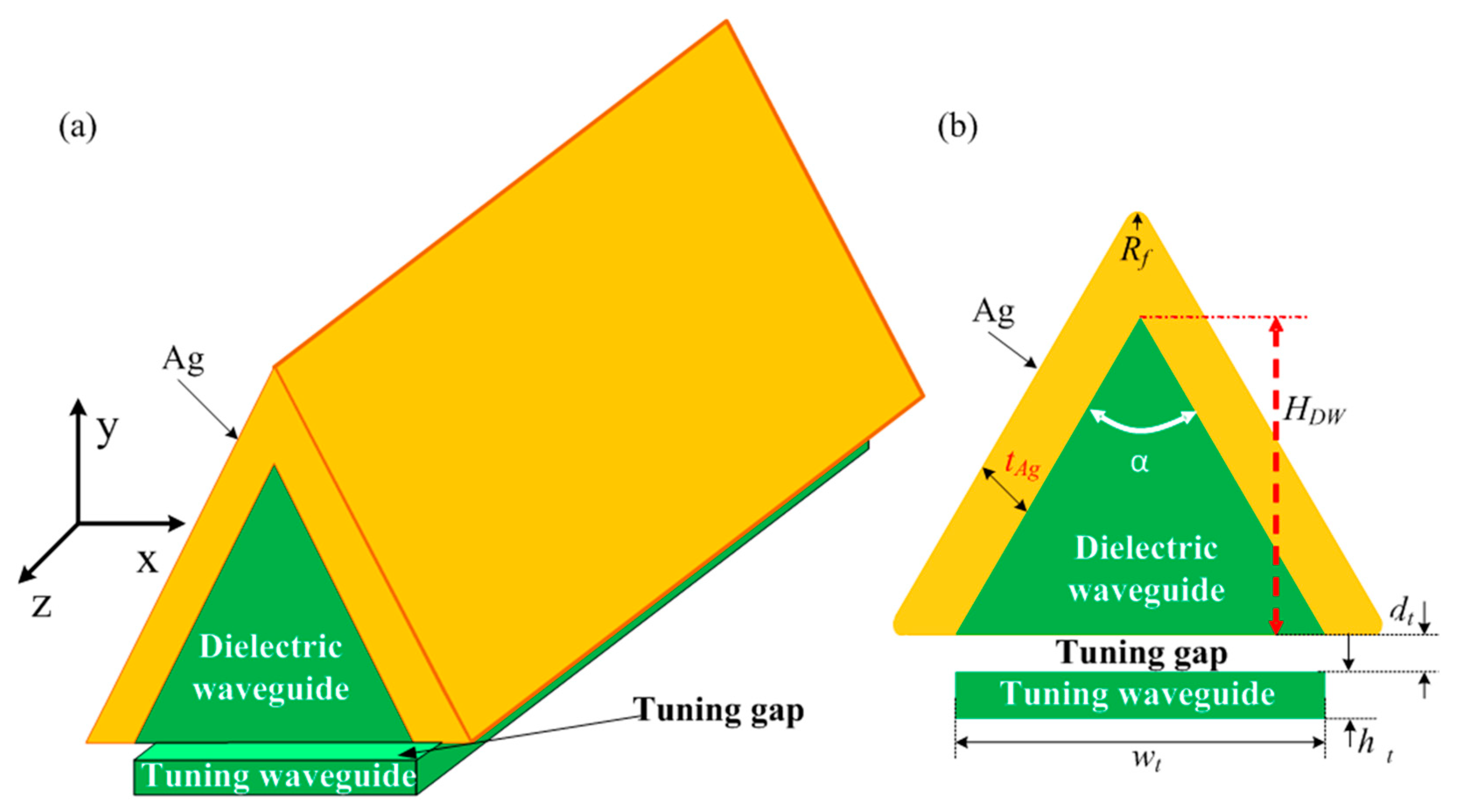
The proposed model of the tunable wedge plasmonic waveguide is shown in
Figure 1.
Figure 1a is a three-dimensional model of the tunable wedge plasmonic waveguide, while
Figure 1b shows the cross-sectional view of the device in the xy plane to denote the dimensional parameters of the device. The device is composed of a dielectric waveguide covered by an Ag metal layer for guiding plasmon waves. The dielectric waveguide has a wedge shape, which forms the V-groove metal layer. In previous studies, Ag metal has been shown to be better for surface wave guiding and plasmon resonance enhancement than other metals; however, it is unstable under ambient conditions [
42,
45]. This issue leads to degradation of the performance of plasmonic waveguides as well as Ag-based plasmonic substrates. To solve this problem, one usually uses a thin layer of Au to cover the Ag layer. Although the surface wave guiding property of Au is not as good as that of Ag, it has excellent chemical stability and biocompatibility. Moreover, the investigated results show that the propagation length of surface plasmon polaritons using the Au/Ag double-layer structure with an appropriate thickness of the Au-covering layer can be increased by a factor of 4 compared to that of using only the Au metallic structure at the same propagation mode area [
45]. The Au/Ag double-layer structure can also be used for designing the present waveguide without affecting the general archives of the study. Furthermore, there are various investigations on applications of both graphene and metals in plasmonics [
36,
37,
38,
39]. However, there is much debate regarding whether graphene is more suitable than metals for use in plasmonics [
36]. For metals, the conductivity is constant; therefore, the surface plasmon characteristics are fixed. In contrast, the conductivity in graphene depends on temperature, chemical potential, relaxation time and radian frequency. The operation range of graphene material is from the microwave to the mid-infrared regimes. In contrast, metal structures are mainly used in the visible and near-infrared regions. Graphene’s conductivity tunability has been widely utilized for developing reconfigurable optical devices [
36,
37,
38,
39,
40]. Notable research on the comparison of SPP transmission between graphene and noble metals as conductors for plasmonic one-dimensional waveguides is carried out in Ref. [
41]. The investigation showed that with plasmon waves at the wavelength of 30 THz, the SPP propagation length of a hybrid insulator–metal–insulator (HIMI) waveguide is lower compared with that of a hybrid insulator–graphene–insulator (IGI) waveguide. This was explained by the fact that silver has a larger negative real part of permittivity than graphene. The graphene complex conductivity is calculated by the well-known Kubo formula within the linear response theory. The permittivity of metals is described by the Drude model. Therefore, losses in graphene are less than silver in the frequencies of a terahertz regime (0.3–10 THz) and a mid-infrared regime (10–100 THz). However, the investigated results of the Ag permittivity are shown in a larger frequency region than 70 THz instead of near-infrared regions covering the frequency of 1.93 THz (i.e., at the optical telecommunication wavelength of 1.55 µm). The operational frequency ranges of Ag and graphene are different, and are considered to be complementary [
36]. In this study, we use the Ag metal for investigating the tuning mechanism proposed for the wedge plasmonic waveguide at the optical telecommunication wavelength of 1.55 µm.
In practice fabrication, flat waveguide structures can be fabricated in a simpler way compared with wedge structures. However, the advantage of wedge plasmonic waveguide structures compared with other plasmonic waveguide structures is their outstanding capacity in tight field confinement, which comes from the strong field confinement around the metal tip structure. Moreover, it is not easy to fabricate wedge structures in plane. Most of the studies on wedge plasmonic waveguides are in vertically integrated types [
20,
21,
26]. To fabricate the proposed wedge plasmonic waveguide, we can form the tuning waveguide and the metal-covered wedge dielectric waveguide on two different wafers, and then assemble them together to form the proposed device.
In previous studies, the metal layer is thick enough so that the plasmon propagation characteristics are not affected by the dielectric waveguide [
21]. This is explained by the SPP waves propagated on the surface of a metal film having an evanescent field penetrating into the metal layer. For the thin metal film, SPP waves propagating on two surfaces of the thin metal film will couple with each other. In addition, the height of the dielectric waveguide (dielectric core in Ref. [
43]) is high enough to eliminate interference between the SPP modes at the interface between the metal layer and the dielectric waveguide and the SPP modes at the air medium and metal layer interface. Moreover, for the wedge plasmonic waveguides, the propagation characteristics are usually tuned by modifying the properties of the dielectric layer covered on the metal layer [
28,
29,
30,
31,
32]. However, in this work, we study the tunable capability of the wedge plasmonic waveguides by modulating the SPP modes at the interface between the metal layer and the dielectric waveguide. This is carried out by tuning the effective RI of the dielectric waveguide. To tune the index of the dielectric waveguide, one can use tuning mechanisms such as thermo-electric, electro-optic or electromechanical tuning [
27,
28,
29,
30,
31,
32]. Here, we use the electromechanical tuning mechanism as reported in Refs. [
32,
44], in which the RI of the dielectric waveguide is tuned by using a closely coupled tuning waveguide (
Figure 1). The physical basis of the tuning mechanism is explained based on modifying the RI of the dielectric waveguide. When the RI-tuning waveguide is moved close enough to the dielectric waveguide, the effective RI of the dielectric waveguide is modulated. Therefore, it changes the mode properties of SPP waves propagating at the interface between the metal layer and the dielectric waveguide. Consequently, the WPP mode properties of SPP waves propagating at the interface between the metal layer and the air dielectric medium are modulated. The strength of modulating the WPP mode characteristics can be tuned by varying the distance between the RI-tuning waveguide and the dielectric waveguide. Here, we consider three characteristic propagation parameters which are effective mode index (
Neff), propagation length (
LWPP), and effective mode area (
Aeff). The propagation properties of SPPs in the device are described by Maxwell’s wave equations [
46]. In the case of the absence of an external electric field (the electric displacement D = 0) and the negligible variation of the dielectric constant or relative permittivity
ε =
ε(
r) over distances on the order of one optical wavelength, the wave equation for investigating the propagation properties of surface plasmon polaritons is given by
in which
r is the position in the Cartesian coordinate system,
E(
r,
t) is the electric field depending on
r and time
t, and
c is the speed of light in vacuum.
It is assumed that the electric field of propagating waves has a harmonic type depending on time such as
= E(
r)e
−iωt. Inserting the expression of
into Equation (1), the wave equation is derived as
where
k0 =
ω/
c is the wave vector of the wave with the angular frequency
ω propagating in vacuum. To derive a concrete wave equation to describe the propagating waves, we define a Cartesian coordinate system for an interface between the metal and the dielectric medium as follows: z is the direction of the propagating wave, y is the direction perpendicular to the interface, and x is the direction in the interface plane. Therefore, the propagating waves can be described as E(
x,y,
z) =
E(
y)
eiβz;
β is the complex propagation constant
β =
kz of the traveling waves and corresponds to the component of the wave vector in the direction of propagation. Inserting this expression into Equation (2) yields the following wave equation
By the finite element method [
23], we can find the propagation constant of WPP mode that satisfies
Equation (3) for each space region in the device. The boundary mode analysis
problem in the COMSOL Multiphysics software Version 5.5 is used to solve the
propagation constant of the electromagnetic wave [
21,
23]. The effective mode index
Neff is the real
part of the complex index
neff in which
neff is determined by
β,
neff
=
β/
k0. The
propagation length of the WPP mode is defined as
LWPP = 1/Im(
β) and calculated by
LWPP =
λ0/[2πIm(
neff)]. The
effective mode area is calculated via expression
The propagation characteristics of the device are evaluated at the telecommunication wavelength
λ0 of 1.55 μm. At this wavelength, the complex RI of Ag is 0.15649–1.567i. Furthermore, to avoid abnormal sharp edge effects and for suitability with practice fabrication, the apex angle of the device is filleted with a radius of
Rf (as shown in
Figure 1). In this study, we use
Rf = 2 nm for all simulations. The simulation model is three-dimensional with the calculation size of 4 × 4 × 10 µm
3. Two boundary ports are applied on the back and front face of the waveguide to analyze modes that can propagate in structure. The perfectly matched layer is larger than the calculation domain by five times and the minimum mesh size is about 1 nm (near the apex of the waveguide and in the metal layer). The SPPs are excited at
λ0 = 1.55 μm by a transverse electric (TE) wave propagating along the z axis at the input port with an input power of 1 W. The phase of the excited TE wave is set at 0 rad. In simulation, we apply the excited TE wave on the whole input port; therefore, the density of power is 62.5 mW/μm
2.
3. Tunable Characteristics of Wedge Plasmonic Waveguide
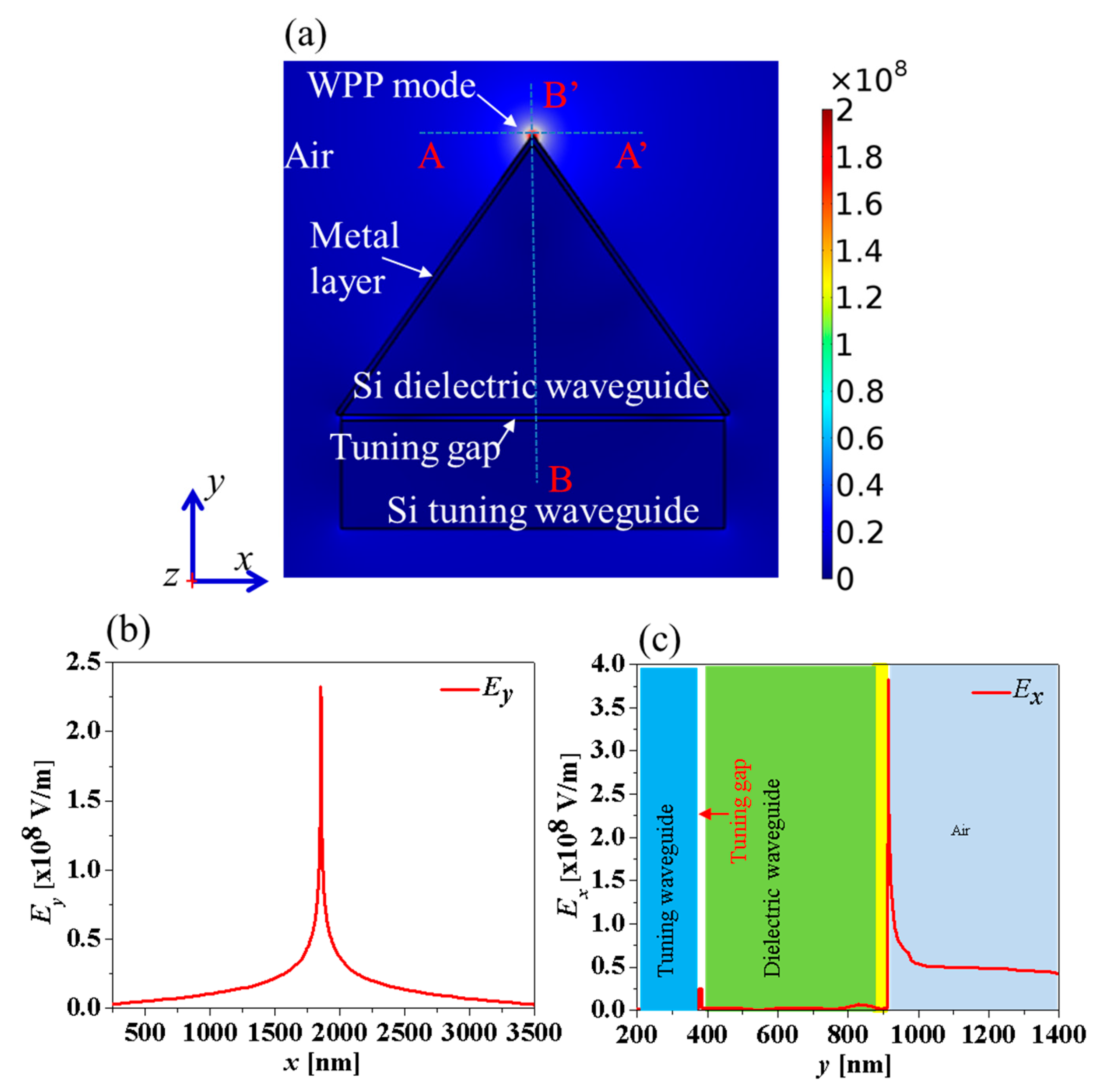
Normalized total electric field distribution of the wedge plasmonic waveguide with the Ag layer with a thickness of 10 nm is shown in
Figure 2a. Electric field profiles across the apex of the device along the x and y axis are shown in
Figure 2b,c, respectively. It is clear that the electric field is distributed mainly in the air region on the apex of the device and it decreases quickly from the apex into the air region (
Figure 2b,c). This propagation mode is called WPP mode [
19,
20,
21,
43]. The WPP mode is the coupling mode formed by two SPP waves propagating toward the apex on the two opposite faces of the metallic wedge [
47]. The group velocity tends to zero, while the wave vector tends to infinity at the apex. This leads to an infinitesimal mode size or nanofocusing. The propagation characteristics of this mode for the thin and thick metal films have been investigated [
21,
43]. When the height of the wedge plasmonic waveguide increases, the propagation mode size is decreased. The decrease in the propagation mode size leads to a reduction in propagation length or an increase in propagation attenuation. This is a trade-off between the mode confinement and the low-loss propagation in plasmonic waveguides [
19,
46]. When the apex angle of the metal wedge increases, the propagation mode size is expanded while the propagation length increases [
21,
43]. In this study, we will focus on investigating the propagation characteristics of the wedge plasmonic waveguide by modifying the effective RI of the dielectric waveguide that shapes the V-groove type metal layer (metallic wedge) (
Figure 1). Without affecting the derived study results, we fixed the apex angle α at 70° in all simulations. This typical apex angle is derived from the wet anisotropic etching property of single crystal silicon in a potassium hydroxide solution. Using this wet anisotropic etching property, we can obtain the typical apex angle of the wedge dielectric waveguide α = 70° [
21]. The effective RI of the dielectric waveguide is tuned using a closely suspended tuning waveguide. In Ref. [
43], the modes propagating in the V-groove metal layer plasmonic waveguide include the WPP modes and the channel plasmon polariton (CPP) modes. The properties of these modes depend on the apex angle and the width of the side surface, i.e., the height of the dielectric waveguide. In Ref. [
43], the height of the dielectric core, which is the dielectric waveguide in this study, is chosen to be larger than 5 μm to eliminate interference of the geometrical dimensions to the propagation characteristics. The investigated results show that the propagation characteristics of the WPP mode do not depend on variation of the dielectric constant as well as the refractive index of the dielectric waveguide. Here, the refractive index is related to the dielectric constant by the expression
n =
. In this work, we study the propagation characteristics of the device in the case that the geometrical dimension of the dielectric waveguide interferes with the WPP modes. The physical nature of modifying the geometrical dimension of the dielectric waveguide is to modulate its effective RI. In the following sections, we present the investigated results of modifying the propagation mode properties using an RI-tuning waveguide suspended under the dielectric waveguide (
Figure 1).
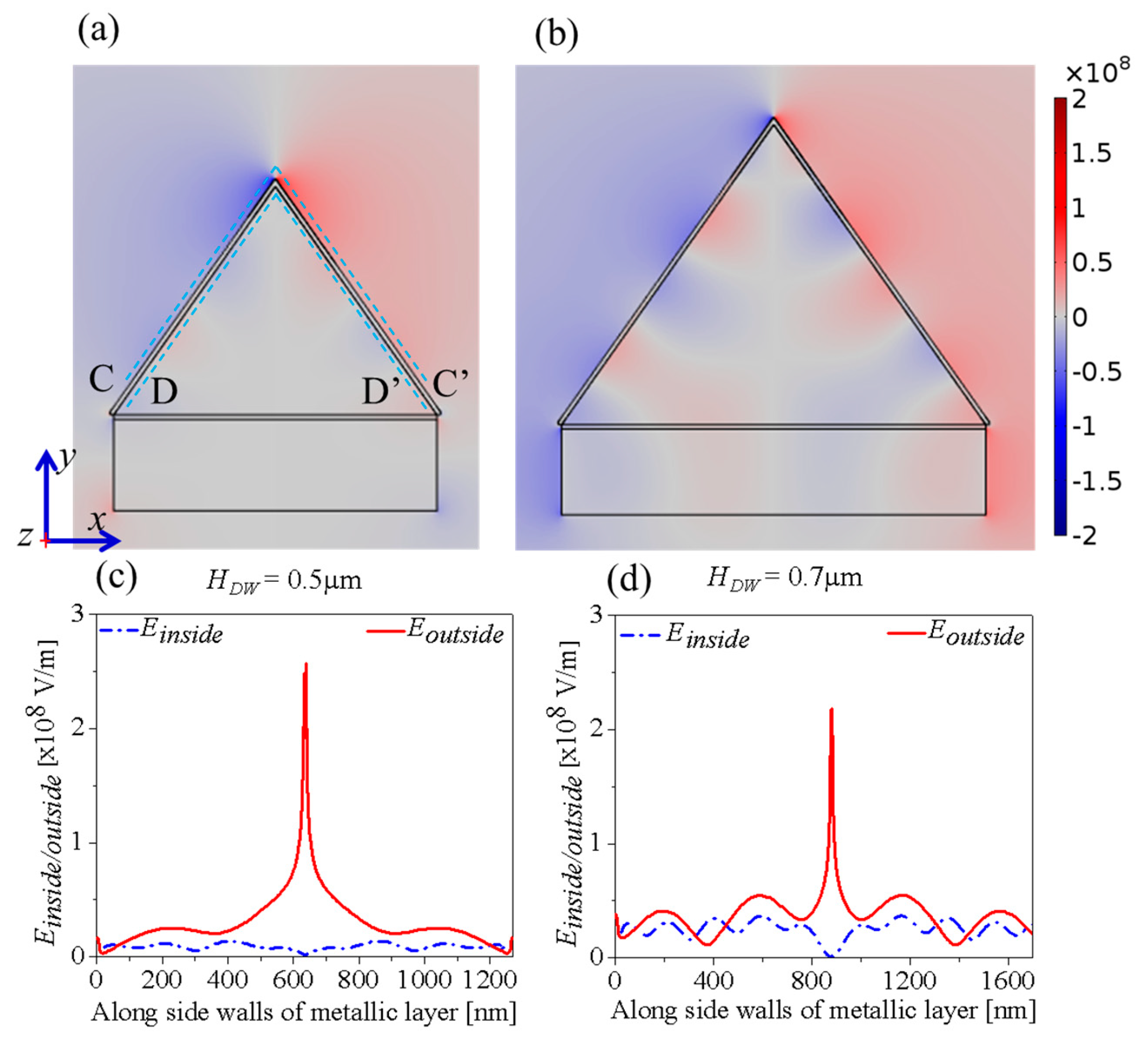
Figure 3a,b show the electric field distribution of the wedge plasmonic waveguide along the x direction for two heights of the dielectric waveguide,
HDW = 0.5 µm and
HDW = 0.7 µm, respectively. It is clear that there are two SPP mode types propagating at the inside surface and the outside surface of the V-groove metal layer with the Ag metallic layer having a thickness of 10 nm. These SPP modes are coupled with each other when the metallic layer is thin enough. The strength of modes coupling depends on the penetration depth of the evanescent field through the metallic layer [
46]. The coupling strength between the two modes propagating at both sides of a flat metal film (DMD structure, i.e., a thin metallic film sandwiched between two dielectric layers) depends on the penetration depth of the evanescent field, at which the field falls to 1/e, determined by δ =
[
46], where
is the wave number in vacuum,
is the real part of the complex dielectric constant of metal, and
is the dielectric constant of dielectric. The implicit expressions for the field components depending on permitivities and propagation constants in each region of the DMD structure have also been derived in [
46]. However, in the design of the wedge plasmonic waveguide structure (the V-shaped DMD structure) with the non-flat metal/dielectric interface, we choose the thickness of the metal layer much less than that of the flat interface. In the flat interface, with
= −129 for Ag and
= 12.25, δ is calculated to be 330 nm. In addition, we also refer to Ref. [
43] for choosing the thickness of the metal layer. After choosing the suitable thickness of the metal layer for an effective interaction between the two modes, we modify the index of the dielectric waveguide by varying the distance between the tuning waveguide and the dielectric waveguide. The propagation characteristics of these modes depend on the height of the dielectric waveguide or the side surface width of the V-groove metal layer, in that its physical nature is the dependence on the RI of the dielectric waveguide.
Figure 3c,d show electric field profiles of the device along the side walls of the V-groove metallic layer at a distance of 2 nm above (the folded line CC’) and below (the folded line DD’) the V-groove metallic layer (
Figure 3a) for
HDW = 0.5 µm and
HDW = 0.7 µm, respectively. The amplitude of electric field intensities of SPP modes inside the V-groove metallic layer is much smaller (one order of magnitude lower) than that of SPP modes outside the V-groove metallic layer (WPP mode).
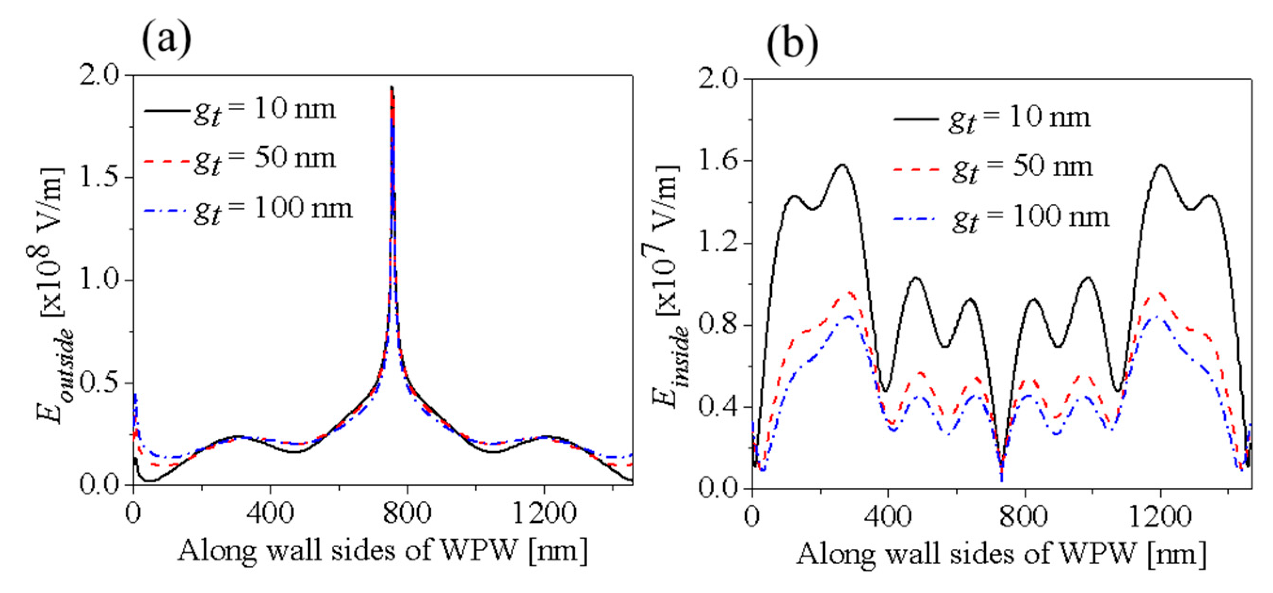
Figure 4a,b present electric field profiles of the wedge plasmonic waveguide along the folded line CC’ (
Figure 3a) and along the folded line DD’ (
Figure 3a) for three tuning gaps,
gt = 10 nm, 50 nm, and 100 nm, respectively. Thus, the electric field profiles of the WPP modes are almost unchanged while the field intensity is slightly reduced during displacement of the RI-tuning waveguide. The electric field profiles of the SPP modes inside the V-shaped metal layer are also unchanged while the strength of field intensities of the SPP modes is decreased and tends to approach asymptotic behavior with the increase of
gt. When
gt is large enough, the dielectric waveguide and the RI-tuning waveguide become independent without coupling. Under this condition, the SPP modes in the V-groove metal layer behave as a normal passive wedge plasmonic waveguide.
In the following, we present variation of the mode characteristics,
Neff,
LWPP, and
Aeff, on
gt.
Neff,
Aeff, and
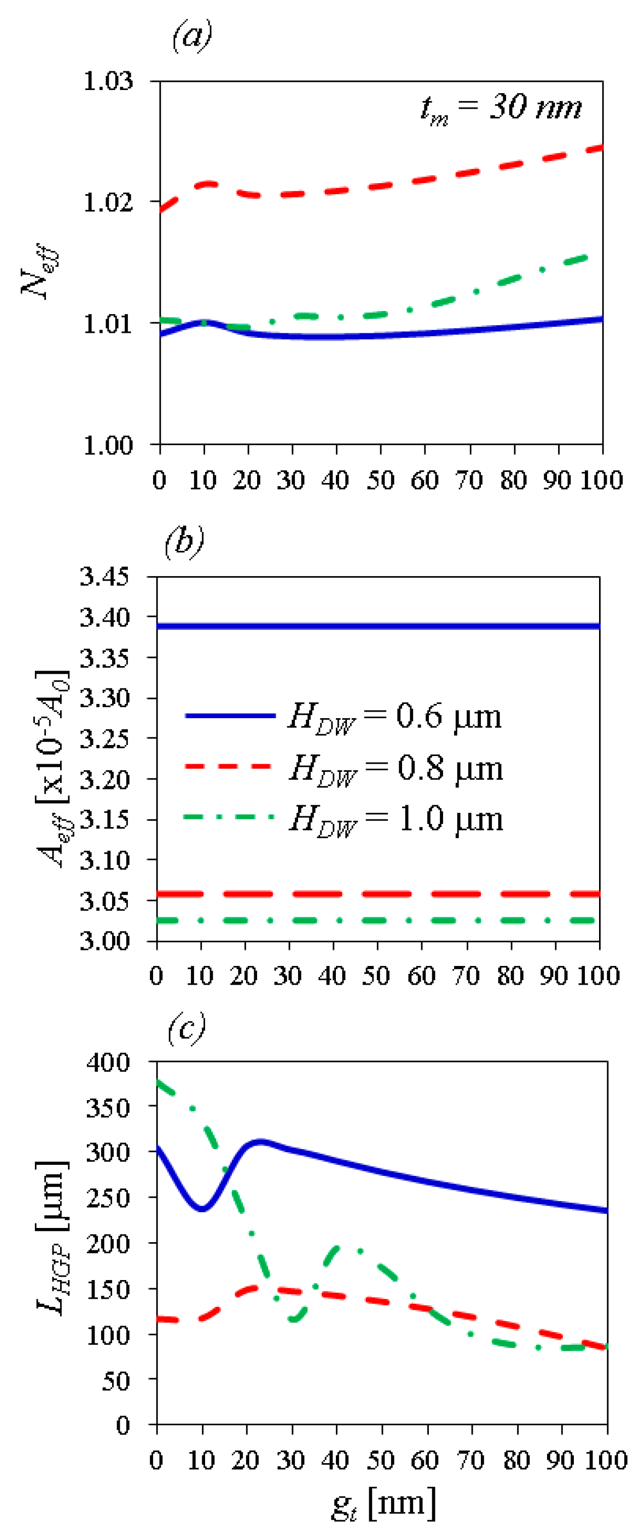
LHGP, investigated as a function of
gt for three different values of
HDW,
HDW = 0.6 μm, 0.8 μm, and 1.0 μm, are shown in
Figure 5a–c, respectively. At the beginning of tuning
gt, the
Neff and
LWPP curves appear as peaks (
Figure 5a,c). The appearance of the characteristic peaks can be affected by changing the geometrical structure and the field coupling between the dielectric waveguide and the RI-tuning waveguide when the gap is changed. After the peaks appear,
Neff increases slightly (
Figure 5a) while
LWPP decreases (
Figure 5c). It is noticed that while tuning
LWPP,
Aeff with the deep-subwavelength size (on the scale of 10
−5 A0 (=5.6 × 10
−6 μm
2), here
A0 (=λ
2/4) is the diffraction-limited mode area in free space) is kept constant. The propagation length is tuned quite linearly after the peaks, especially for the wedge plasmonic waveguides with the small values of
HDW (
HDW ≤ 0.8 μm).
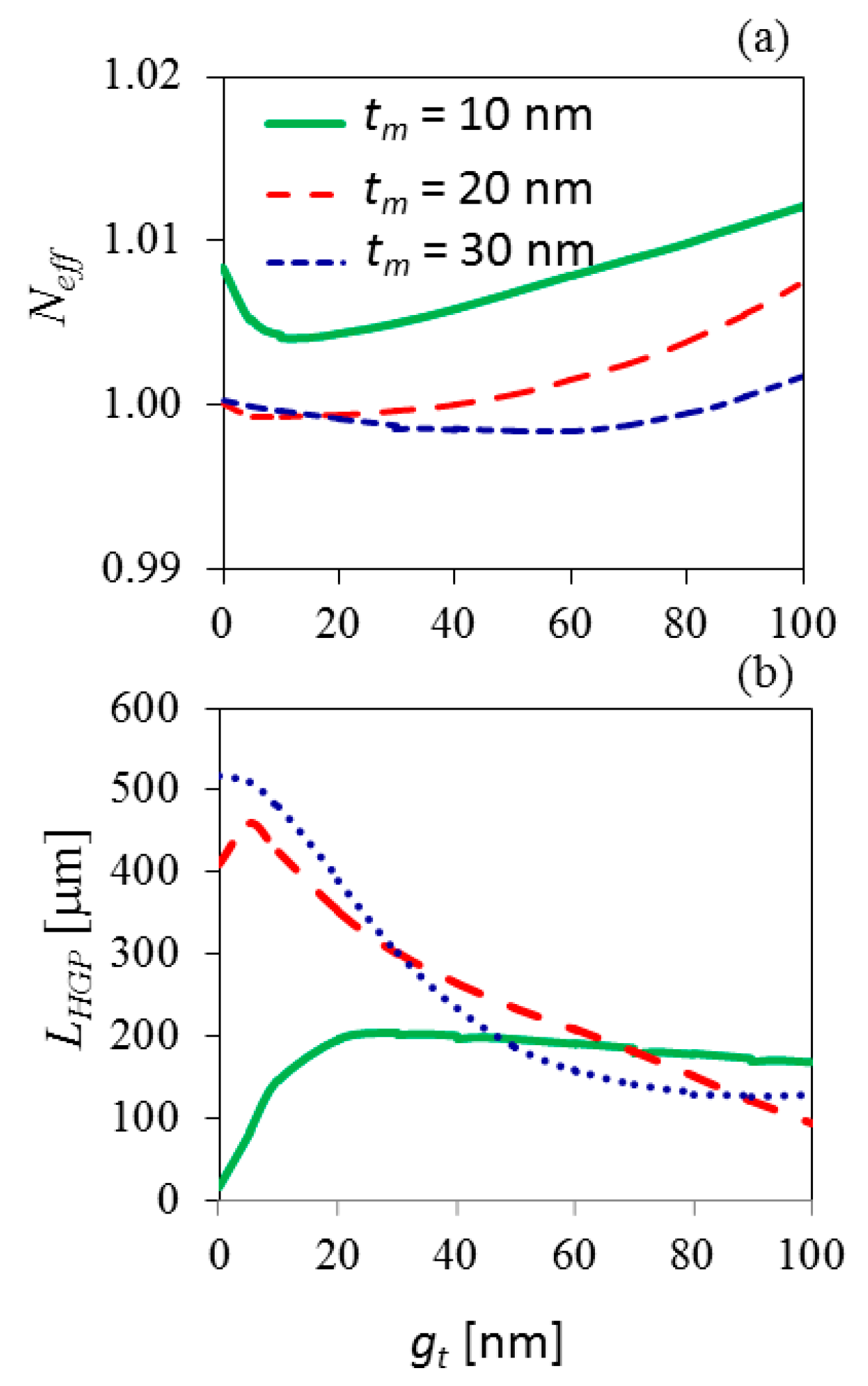
Figure 6a,b, respectively, present the investigated results of
Neff and
LHGP depending on
gt for three different values of
tm,
tm = 10 nm, 20 nm, and 30 nm. At the initial displacement of the RI-tuning waveguide,
Neff decreases, then it increases (
Figure 6a), while
LWPP increases and approaches a maximum value at small
tm values, then decreases with the increase of
tm (
Figure 6b). However, at large t
m values, the peaks disappear. It is clear that at the small
tm values,
LWPP increases strongly with
gt, from 50 μm to 200 μm, i.e.,
LWPP increases 150%. On the decreasing side of the
LWPP curves,
LWPP shows a quick reduction with the increase of
gt for large
tm values. For example, at
tm = 30 nm,
LWPP decreases from the highest value of 500 μm at
gt = 0 nm to an asymptotic value of 120 μm at
gt = 70 nm, while at
tm = 20 nm,
LWPP increases a bit at the beginning, then it decreases quite linearly with
gt, from 470 μm to 100 μm (
Figure 6b). Unlike the previously reported results [
43], the propagation length of the wedge plasmonic waveguide in this study is strongly modulated, more than 100%. The physical nature of convex curves for the small
tm values can be explained as follows. The electric field energy strongly concentrates at the interface between the metal film and air medium (low-RI dielectric media); a part of the electric field energy also concentrates on the interface between the metal film and silicon dielectric waveguide (high-RI dielectric media). When
gt increases, the RI of the dielectric waveguide decreases [
32], which leads to reducing the attenuation of the SPP waves propagating on the interface between the metal film and silicon dielectric waveguide. Moreover, a part of the electric field energy of the device is transferred into the tuning gap, which is considered to be less lost than compared with the SPP waves propagating at the metal-dielectric interface; therefore,
LWPP increases. However, when
gt further increases, the energy storing in the tuning gap is transferred into the metal–dielectric interface; therefore, the propagation length decreases.
Thus, we have proposed and investigated the tunable propagation characteristics of a wedge plasmonic waveguide based on modulating the RI of a wedge dielectric waveguide using a closely coupled tuning waveguide. The numerically investigated results have shown that the propagation length of the device can be tuned more than 100%. The propagation mode area is not changed while tuning the propagation length. The proposed wedge plasmonic waveguide can be applied as a wave guide at telecommunication wavelengths with deep-subwavelength mode size [
19,
20,
43]. It can also be used for optical signal modulating devices [
48]. Furthermore, we proposed to use electrostatic actuation based on capacitance structure to control the gap between the tuning waveguide and dielectric waveguide. The power consumption of this actuation method is negligible due to the operation with low electric current. To reduce losses and improve the performance of the waveguide, we can reduce the actuation gap. In this case, the propagation length of the waveguide is increased, i.e., decreased loss in the device, while the propagation mode area is almost unchanged.
