Abstract
Augmented reality overlays computer-generated virtual information onto real-world scenes, enhancing user interaction and perception. However, traditional augmented reality optical systems are usually large, bulky, and have limited optical performance. In this paper, we propose a novel compact monochrome reflective dielectric metalens visor with see-through properties, engineered using a periodic structure of spin-dependent supercells. The supercell, which is composed of staggered twin nanofins, provides spin-dependent destructive or constructive interference with different circularly polarized incidences. The design combines the principles of interference with the Pancharatnam–Berry phase to enhance reflection at a working wavelength of 650 nm while maintaining good transmission. Right circularly polarized light incident from the substrate side causes destructive interference, enabling the supercell to work in reflection mode, while left circularly polarized light causes constructive interference, enabling the supercell to work in transmission mode. Furthermore, the supercell-constructed metalens can achieve near-diffraction-limited reflective focusing and a broad diagonal field of view of approximately 96°. In addition, compared to transmissive metalens visors, the reflective design eliminates the need for a beam splitter, significantly reducing the size and weight of the system. Our work could facilitate the development of compact and lightweight imaging systems and provide valuable insights for augmented reality near-eye display applications.
1. Introduction
Recently, augmented reality (AR) technology has been rapidly developing and showing great potential in fields such as entertainment, education, and healthcare [1,2,3,4,5,6,7]. AR brings a new immersive and interactive experience to users by fusing virtual information with the real world. However, current AR display systems, especially optical systems, generally suffer from a large size, heavy weight, and a narrow field of view (FOV). These problems mainly result from the physical size and design limitations of traditional optical elements. Conventional optical elements, such as refractive lenses and diffraction gratings, require long optical paths and complex optical systems, making it difficult to realize lightweight and compact AR optical systems, which affects a user’s immersive experience. Therefore, it is important to develop new optical elements to address these issues.
Metasurfaces composed of subwavelength structures have attracted widespread attention due to their ultra-thin and flexible wavefront control capabilities [8,9,10,11]. Various metasurface elements have been studied, including lenses [12,13], wave plates [14], gratings [15,16], and holograms [17,18,19]. Metalenses can achieve light focusing in an ultra-compact form factor and have been studied in many fields, such as imaging [20,21,22], fiber-optic communications [23], and sensing [24,25], providing new ideas for the design of compact AR systems. Lan et al. introduced a holographic display technology for AR, which can project virtual information directly onto the retina but requires a transparent display [26]. In 2018, Lee et al. proposed a method of combining a transmissive metalens with a beam splitter as an eyepiece in an AR system [27]. In 2021, Wang et al. presented a silicon nitride nanofin array metalens combined with three-dimensional computational holography for a holographic near-eye display system [28]. In 2022, Li et al. proposed an inverse design framework for a see-through metalens combined with a beam splitter for use in AR and VR near-eye systems [29]. However, metalenses usually require additional beam splitters to achieve the dual functions of reflecting virtual images and transmitting real scenes. This combination increases the complexity and weight of the system, weakening the advantages of metasurfaces in achieving a light and compact design.
The design of near-eye display systems based on reflective metalenses has been pro-posed recently. Virtual images are reflected into the human eye through the metalenses instead of beam splitters. This approach allows for more compact form factors. Hong et al. designed a planar reflective off-axis metalens based on Zernike polynomial phase distribution, but it required a multilayer composite structure for reflection [30]. Nikolov et al. introduced a metasurface, which integrates the combined advantages of freeform optical elements and metasurfaces into one optical element but uses a metallic silver layer to achieve reflection [31]. Yan Li et al. proposed a single-layer reflective metalens design that achieved a large field of view, but it used high-reflectivity nanofins at the expense of transmittance at the working wavelength [32]. Song et al. introduced a transparent non-local metasurface that provides high transparency in the visible light spectrum and reflects near-infrared light for eye tracking, making it unsuitable for visible light imaging [33]. Therefore, although reflective metalenses can be more compact, further research is needed to develop more effective design methods for achieving both reflection and transmission.
In this paper, we propose a novel compact monochrome reflective dielectric metalens visor with see-through properties, utilizing a periodic arrangement of spin-dependent supercells. The reflective mode is designed to operate at a wavelength of 650 nm. The design combines constructive and destructive interference principles with the Pancharatnam–Berry (PB) phase to achieve asymmetric transmission and precise light control. The proposed dielectric supercell for visible light consists of two pairs of nanofins: one single cuboid nanofin and one cross-shaped nanofin composed of two rectangular cuboids. This arrangement enables unique spin-dependent interference under circularly polarized (CP) light. Specifically, right circularly polarized (RCP) light incident from the substrate side induces destructive interference, enabling the supercell to work in reflection mode, while left circularly polarized (LCP) light induces constructive interference, allowing it to work in transmission mode. When CP light is incident from the opposite direction, the transmission or reflection behavior reverses. Compared to using a single simple nanofin as the periodic structure, this unique characteristic of the supercell is highly suitable for AR visor design, offering better reflection and transmission performance with high-transmittance dielectric materials. Furthermore, the metalens constructed from the supercell arrays can achieve near-diffraction-limited reflective focusing and offers a wide field of view of approximately 96°, which is quite large for AR displays [1,2,3]. Moreover, this reflective design eliminates the need for a beam splitter and significantly reduces the size and weight of the system compared to conventional transmissive metal lenses. Operating as a monochrome reflective system, it is particularly suitable for applications that require focused attention on key information, such as industrial guidance, medical surgery, warehousing logistics, and real-time language translation. This work could facilitate the development of thinner and lighter imaging systems and provide new insights into AR near-eye optical systems.
2. Operating Principles
Figure 1a shows a simplified schematic diagram of a transmissive metalens used in an AR optical system. The system consists of a transmissive metalens and a beam splitter, which reflects virtual images while transmitting real scene light. However, the addition of a beam splitter increases both the thickness and weight of the system. In contrast, Figure 1b shows a simplified schematic diagram of a see-through reflective metalens used in an AR optical system. This reflective metalens performs dual functions: it reflects and focuses virtual image light directly into the human eye without the need for an additional beam splitter, and it also transmits real scene light, resulting in a more compact and lightweight visor.
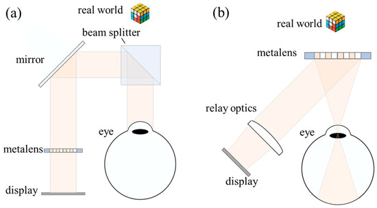
Figure 1.
(a) Simplified schematic diagram of an AR optical system using a transmissive metalens; (b) simplified schematic diagram of an AR optical system utilizing a see-through reflective metalens.
To realize the reflective metalens, we first proposed the design of a supercell applicable for the visible range to achieve circular asymmetric transmission. As shown in Figure 2, the supercell consists of a pair of staggered twin nanofins. Figure 2a shows the two types of nanofins: the blue one is a rectangular cuboid, while the red one is a cross-shaped structure composed of two rectangular cuboids. Figure 2b shows a perspective view of the supercell, and Figure 2c shows a top view of the supercell. When CP light interacts with the supercell, the electric field E caused by collective interference can be expressed as follows [34]:
where represents the phase shift of the blue nanofin, and represents the phase shift of the red nanofin. When , it results in constructive interference, and the supercell operates in transmission mode. Conversely, when , it results in destructive interference, and the supercell operates in reflection mode. The phase accumulation of neighboring nanofins under CP light incidence is .
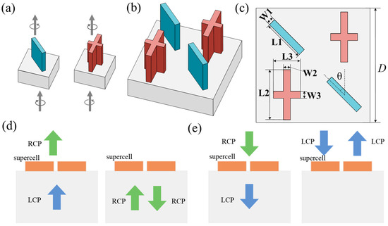
Figure 2.
Schematic diagram of the structure and operating principles of the supercell. (a) Schematic of the two types of nanofins used: a rectangular cuboid (blue) and a cross-shaped structure (red); (b) perspective view of the supercell; (c) top view of the supercell; (d) schematic diagram of the transmission/reflection mode for forward CP light incidence; (e) schematic diagram of the transmission/reflection mode for backward CP light incidence.
In order to realize different operational modes, it is very important to analyze the phase difference between the blue and red nanofins. This phase difference consists of two main components: the transmission phase difference and the PB phase difference . Firstly, the transmission phase is the phase shift caused by the optical path difference when light propagates in different media. The blue and red nanofins have the same height. Therefore, the effective refractive index can be changed by changing the dimensions of the nanofins, resulting in different values of the transmission phase. Secondly, the rotation of the nanofins contributes to the PB phase. When the CP light is incident on a single nanofin, the transmitted light can be expressed as follows [24]:
where σ represents the spin state of CP light, with +1 for LCP incidence and -1 for RCP incidence. denotes the unit vector for either CP and . and are the complex transmission coefficients of linearly polarized light along the longer and shorter axes of the nanofin, respectively. θ is the orientation angle along the z-axis. As defined by Equation (2), the transmitted light consists of two components, namely co-polarized and cross-polarized. The cross-polarized component experiences a relative phase shift of 2σθ, referred to as the PB phase. Polarization conversion efficiency measures the performance and energy loss of an optical device in converting the polarization state of incident light. A high efficiency indicates that most of the energy of the incident light is used for the intended polarization conversion, resulting in a high-intensity output light. Therefore, it is necessary to select nanofins with a very high polarization conversion efficiency. Consequently, the total phase difference ∆φ can be expressed as follows:
The transmission phase difference is set to −π/2 and the orientation angle θ to 45°. When LCP light is incident on the supercell from the substrate side, ∆φ equals 0, resulting in constructive interference. Peaks align with peaks and troughs with troughs, enhancing transmission and allowing more energy to pass through. The supercell can operate in transmission mode, as shown in Figure 2d (left). When RCP light is incident, ∆φ equals -π, resulting in destructive interference. Peaks cancel out troughs, suppressing transmission and causing most of the energy to be reflected, thereby enhancing reflection. The supercell can operate in reflection mode, as shown in Figure 2d (right). When CP light is incident from the reverse direction, the transmission and reflection modes will be reversed, as shown in Figure 2e. Therefore, by combining the principles of the transmission phase, PB phase, and interference, supercells can achieve asymmetric transmission. The operating principles provide theoretical support for the design of see-through reflective metalenses.
3. Design and Results of Spin-Dependent Supercells
According to the above analysis of the operating principles, we designed the supercell through a systematic process. The dimensions and period of the nanofins affect the transmission phase value of each nanofin. The period is also the spacing value between nanofins. Therefore, the first step was to scan various shapes, dimensions, and periods of nanofins, obtain their polarization conversion efficiency and transmission phase values, and select those with an optimal polarization conversion efficiency. The second step was to calculate the phase difference by subtracting any two of the transmission phase values from the first step, and selecting the corresponding nanofin pairs with a difference of about −π/2. This phase difference is important to achieve the desired interference effect in the supercell. The final step was to simulate the supercells constructed by the nanofin pairs, and obtain their transmittance and reflectance to determine the most suitable supercell. During the scanning and calculation process, the finite-difference time-domain method was used to ensure accurate modeling of the electromagnetic fields. Moreover, to achieve high reflectivity, it was necessary to have high refractive index contrast at the interface. Silicon, which is a high refractive index material, has been used for nanofins to realize high-performance metalenses [35,36]. Crystalline silicon, in particular, is better suited for visible light applications than amorphous silicon because of its excellent optical transparency and lower optical loss, and has been explored as a material platform for high-efficiency metalenses [37,38]. Therefore, crystalline silicon was chosen for the nanofins. The material of the substrate was SiO2.
Two types of nanofins were finally selected: a single cuboid nanofin and a cross-shaped nanofin composed of two cuboids, with detailed dimensions shown in Figure 2c. W1 and L1 are the width and length of the blue nanopillar, respectively. W2 and L2, and W3 and L3 are the width and length of the two cuboids that construct the red nanofin, respectively. The size D of the supercell is 640 nm. The dimensions are as follows: W1 = 40 nm, L1 = 235 nm, W2 = 40 nm, L2 = 280 nm, W3 = 40 nm, and L3 = 150 nm. The nanofins have a height of 430 nm, a spacing of 320 nm, and a transmission phase difference of about -π/2. Their polarization conversion efficiencies both exceed 90%. Selection and optimization ensured excellent phase control and polarization efficiency. Figure 3a shows the simulated transmission spectrum of the supercell. It shows that a certain green spectrum has a transmittance over 50%, and for the red spectrum over 70%. This shows that the transmittance is good compared to other reflective display methods. After balancing the reflection and transmission performance, we chose a design wavelength of 650 nm. Considering that the narrow bandwidth of monochrome displays is between 10 nm and 20 nm, we simulated and analyzed the reflectivity of the selected supercell structure within a 20 nm bandwidth centered at 650 nm. The results in Figure 3b show reflectivity greater than 50% within the 20 nm bandwidth and more than 60% within the 10 nm bandwidth. This shows that our design is suitable for typical monochrome displays, ensuring stable performance across the relevant spectral range. As shown in Figure 3c, the reflectance exceeds 70% at a normal incidence and remains above 50% at the design wavelength over a range of incidence angles from 0° to 45°. The critical angle for total internal reflection at the SiO₂–air interface is 44.2°. In the next section of the metalens design, the incident light entered the substrate from the air and then entered the nanofins. The refraction angle of the 43° incident light was 27.91°, which is not close to the critical angle and will not cause total internal reflection. Additionally, when the incident light was reflected, the leakage rate at 0° incidence was 12.2%, while at 43° incidence it was 11.5%, which is within the acceptable range for typical AR devices. As a result, although the dielectric material chosen for the nanofins has a high transmittance, the carefully designed supercell structure not only overcomes the limitations of the material in achieving reflective functionality but also succeeds in achieving polarization-dependent reflections while maintaining a high transmittance at the working wavelength.
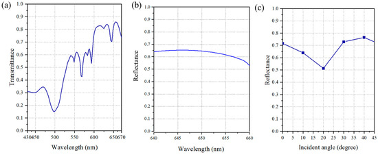
Figure 3.
Characteristics of the supercell. (a) The simulated transmittance varies with wavelengths from 430 nm to 670 nm; (b) the reflectance of the selected supercell structure within a 20 nm bandwidth centered at a wavelength of 650 nm; (c) the simulated reflectance as a function of the incident angle, ranging from 0° to 45°.
Table 1 presents the transmittance and reflectance of RCP light incident from various directions onto different periodic structures at the working wavelength of 650 nm. Compared to using blue and red nanofins as the periodic structure, the selected supercell significantly enhances both reflectance and transmittance. When RCP light propagates along the +z direction and enters the supercell from the substrate, the transmission phase difference between the nanofins is approximately −π/2, with a rotation angle difference of 45°, resulting in a PB phase difference of −π/2. This setup leads to a total phase difference of π, producing destructive interference and increasing reflectance to 68%, over that of other periodic structures. The corresponding light field distribution is shown in Figure 4a. When RCP light is incident along the −z direction, constructive interference occurs, increasing transmittance to 76%. The corresponding electric field distribution is shown in Figure 4b. These results not only demonstrate the supercell’s capacity to control light but also highlight its advantages over traditional periodic structures with single nanofins. Furthermore, improved optical performance makes this supercell design suitable for a metalens visor.

Table 1.
Reflectance and transmittance of periodic structures for RCP light with different directions.
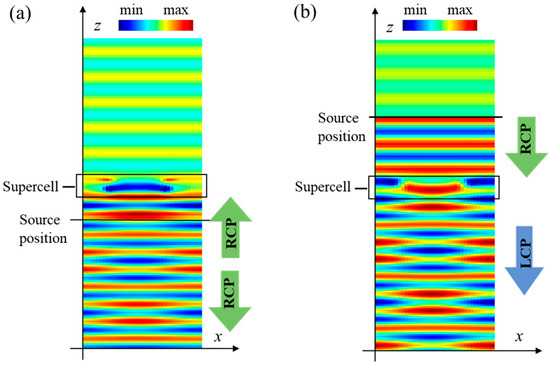
Figure 4.
(a) The distribution of an electric field Ey in the periodic supercell under the illumination of RCP light along the +z direction. (b) The distribution of an electric field Ex in the periodic supercell under the illumination of RCP light along the -z direction.
4. Design and Results of Reflective Metalens
Based on the supercell design in the previous section, we used the spin-dependent supercell to construct the reflective metalens. Unlike traditional transmissive metalenses, this metalens is optimized for reflective focusing effects suitable for light incident at large angles. Specifically, it achieves a wide diagonal field of view of 96° (38° horizontally and vertically). Figure 1b shows a schematic of the AR near-eye optical system using the proposed metalens visor. This system is designed using retinal projection where images emitted from the display are incident off-axis and subsequently reflected and focused into the human pupil by the metalens. Retinal projection projects images directly onto the fovea of the retina, ensuring that light is naturally focused within the eyeball, which better matches the eye’s natural accommodation. This approach reduces the convergence–accommodation conflict, and can significantly reduce visual fatigue when using the device for a long time. In addition, retinal projection can provide a wider field of view [27,28,29]. Figure 5 shows the beam propagation. To realize such optical behavior, we can determine the phase compensation required for each periodic structure on the metalens by calculating the phase delay accumulated during the light’s propagation in different media. The following relationships can be obtained:
where is the incident angle of light; is the refraction angle of light from air to the substrate; is the refractive index of air; is the refractive Sndex of the substrate; is the reflection angle of light; is the refraction angle of light from the substrate into the air; d represents the substrate thickness; f represents the back focal length; x represents the coordinates of each unit; represents the phase of the coordinate origin; and represents the relative phase with respect to the origin of coordinates that needs to be compensated for any periodic structure of the metalens. can be simplified as follows:
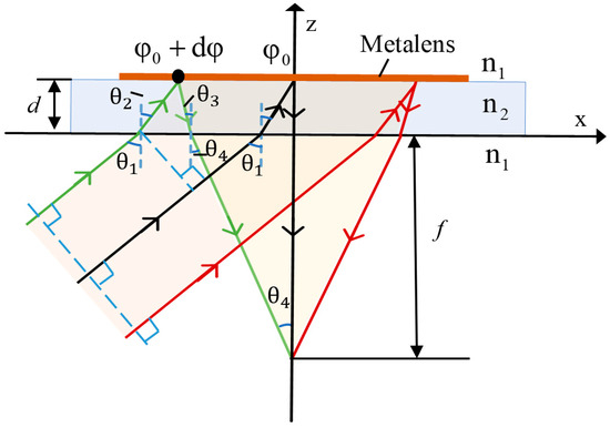
Figure 5.
Schematic diagram of the beam propagation of the metalens.
According to Equation (1), the phase of the output light is half of the sum of the phases of the two nanofins. When the supercell’s twin pairs of nanofins are simultaneously rotated by an angle α as shown in Figure 6a, the phase shift is 2σα. Therefore, we can combine the supercell with the PB phase principle to realize the phase distribution from 0 to 2π by changing the rotation angle. Therefore, we used supercell arrays to construct the metalens and realize the desired phase distribution . When the target diagonal field of view is 96° (76° horizontally and vertically), the back focal length is 4 μm, and the substrate thickness is 0.5 μm; the two-dimensional distribution of the calculated phases is shown in Figure 6b. Due to the large field of view, we used footprint diagrams to approximate the imaging performance as seen by the human eye. We saved the designed phase distribution as a grid phase data file and imported it into Zemax Studio. The imaging effects were visually displayed using a footprint diagram. A footprint diagram is a visual representation commonly used to describe the propagation characteristics of light in optical systems. It is mainly used to show the angular and intensity distribution of light. Figure 6c (left) shows the footprint diagram of light with an incident angle of 43° in the system, describing the initial distribution of the light. Each blue pattern in the figure represents a point light spot, reflecting the initial state and distribution characteristics of the light. Figure 6c (right) shows the footprint diagram at a position 5 μm behind the focal plane. The central part of the diagram is aligned with the optical axis of the phase plane, and the shape of the light spot remains consistent. This indicates that the system can accurately focus light to the intended location without distortion or inconsistency in the output shape. Figure 6d shows a schematic diagram of the metalens constructed from a supercell array. The blue box enlarges a section of the metalens.
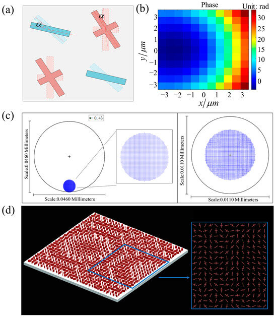
Figure 6.
(a) Schematic diagram of nanofin pairs on the supercell rotated at the same angle α; (b) two-dimensional phase distribution of the metalens; (c) footprint diagram of the incident light (left), and footprint diagram of the output light (right) 5 μm behind the focal plane; (d) structure diagram of the metalens. The blue box shows a scaled-up section of the metalens.
Figure 7 shows the simulation results of the designed metalens, with a working wavelength of 650 nm and an incident angle of 43°. Figure 7a shows the normalized light intensity distribution of the metalens in the x − z plane at y = 0. Figure 7b shows the curve of the light field intensity changing with z when x = 0. It can be clearly seen that the metasurface focuses at z = −4 μm with a long focal depth. Figure 7c shows the normalized light intensity distribution at the focal plane of the metalens. Figure 7d shows the cross-section of the focusing spot with a full width at half maximum (FWHM) of 0.686 μm, which is close to the working wavelength, demonstrating that the metalens we designed can achieve focusing close to the diffraction limit. This near-diffraction-limited focusing not only demonstrates the strong phase control capability of our designed metalens but also shows its potential for high-resolution imaging applications in compact optical systems.
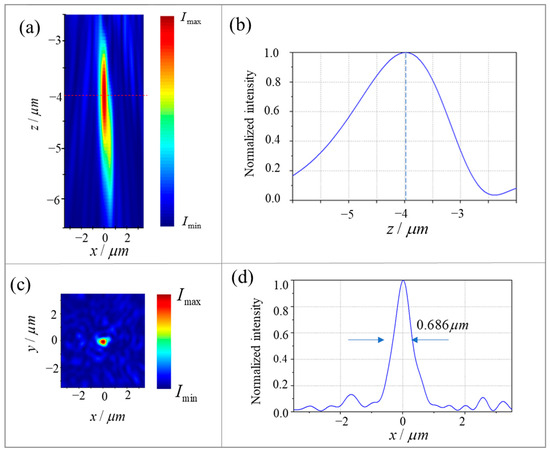
Figure 7.
The simulation results of the designed metalens. (a) Normalized light intensity distribution in the x − z plane at y = 0; (b) the curve of the electric field intensity changing with z at x = 0; (c) normalized light intensity distribution at the focal plane of the metalens when z = −4 μm; (d) cross-section corresponding to the focal spot of the metalens with an FWHM of 0.686 μm.
To verify whether the metalens can maintain good focusing performance as its size increases, we simulated a metalens with a back focal length of 7.5 μm. The incident angle and field of view remained unchanged. Figure 8a shows the normalized light intensity distribution in the x–z plane at y=0, clearly indicating that the metalens focuses at z = −7.5 μm. Figure 8b shows the cross-section of the focal spot. The FWHM is 0.698 μm, which is close to the wavelength and achieves focusing close to the diffraction limit. Figure 8c shows the modulation transfer function (MTF) curves for metalenses with focal lengths of 4 μm and 7.5 μm, respectively, where the red curve corresponds to a 4 μm metalens and the blue curve to a 7.5 μm metalens. The results demonstrate that the metalenses can achieve near-diffraction-limited focusing with good imaging performance as their size increases. Therefore, the metalens can be scaled up and applied to AR optical systems. Moreover, compared to transmissive metalens visors, the reflective solution does not require beam combiners, making it lighter, thinner, and more compact.
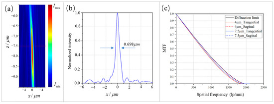
Figure 8.
(a) Normalized light intensity distribution in the x–z plane at y = 0; (b) cross-section of the focal spot, with an FWHM of 0.698 μm; (c) the MTF curves for metalenses with focal lengths of 4 μm and 7.5 μm, with the red curve corresponding to the 4 μm metalens and the blue curve to the 7.5 μm metalens.
5. Discussion and Conclusions
In this paper, we propose a novel compact reflective dielectric metalens visor with see-through properties, achieved using a spin-dependent supercell array. This design method eliminates the need for a beam splitter, making the system more compact and lightweight. By using high-transmittance dielectric materials instead of metals and combining interference principles with the PB phase, the proposed supercell achieves spin-dependent modes for different CP light incidences, operating in reflection or transmission mode as needed. Specifically, when RCP light incident from the substrate side causes destructive interference, the supercell operates in reflection mode at the working wavelength of 650 nm, while when LCP causes constructive interference, the supercell operates in transmission mode. These modes reverse when the light direction is flipped. The supercell we carefully selected shows superior performance, achieving higher reflectance and transmittance compared to conventional single-nanofin periodic structures. At a wavelength of 650 nm, the supercell achieves 68% reflectance for RCP light incident from the substrate side and 76% transmittance from the opposite direction, with high reflectance maintained across incident angles from 0° to 45°. Furthermore, this design offers a simpler structure compared to methods relying on multilayer films for reflection. We constructed the metalens using a supercell array to achieve the desired phase distribution. Results show that the metalens with a back focal length of 4 μm achieves near-diffraction-limited focusing, with an FWHM of 0.686 μm and a broad diagonal field of view of approximately 96° (76° both horizontally and vertically). Furthermore, we verified the focusing performance of the metalens as its size increased. Results showed that even with an increased focal length of 7.5 μm and the same numerical aperture, the metalens maintained near-diffraction-limited focusing and good imaging performance. This scalability makes the design method of the metalens suitable for larger AR near-eye optical systems. In conclusion, our work presents a promising approach for the development of advanced AR systems. We hope that these findings will provide valuable insights and support for future optical system designs. Non-uniform transmittance across the visible spectrum is a common challenge in grating-based and metasurface AR systems, and it remains an important direction for future research. Potential research directions include exploring higher transmittance materials, optimizing nanofin designs, and incorporating advanced optimization techniques.
Author Contributions
Conceptualization, Y.L. and X.W.; methodology, Y.L. and J.L.; software, Y.L. and J.L; validation, Y.L.; formal analysis, Y.L. and J.G.; investigation, Y.L., Q.L. and D.Z.; resources, J.L. and J.G.; data curation, Y.L. and Q.L.; writing—original draft preparation, Y.L.; writing—review and editing, Y.L., Q.L. and D.Z.; supervision, J.L. and J.G.; project administration, X.W.; funding acquisition, J.L. and X.W. All authors have read and agreed to the published version of the manuscript.
Funding
This work was funded by the National Natural Science Foundation of China (62005204, 62075176 and 62005206), Fundamental Research Funds for the Central Universities (ZYTS24094), Natural Science Foundation of Shaanxi Province (2024JC-YBMS-460), and Shaanxi Province Postdoctoral Project (2023BSHEDZZ162).
Institutional Review Board Statement
Not applicable.
Informed Consent Statement
Not applicable.
Data Availability Statement
Data are available on request from the authors.
Conflicts of Interest
The authors declare no conflicts of interest.
References
- Xiong, J.; Hsiang, E.-L.; He, Z.; Zhan, T.; Wu, S.-T. Augmented reality and virtual reality displays: Emerging technologies and future perspectives. Light Sci. Appl. 2021, 10, 216. [Google Scholar] [CrossRef] [PubMed]
- Cheng, D.; Wang, Q.; Liu, Y.; Chen, H.L.; Ni, D.W.; Wang, X.M.; Yao, C.; Hou, Q.C.; Hou, W.H.; Luo, G.; et al. Design and manufacture AR head-mounted displays: A review and outlook. Light Adv. Manuf. 2021, 2, 350–369. [Google Scholar] [CrossRef]
- Yin, K.; He, Z.; Xiong, J.; Zou, J.; Li, K.; Wu, S.-T. Virtual reality and augmented reality displays: Advances and future perspectives. J. Phys. Photonics 2021, 3, 022010. [Google Scholar] [CrossRef]
- Zhan, T.; Yin, K.; Xiong, J.; He, Z.; Wu, S.-T. Augmented reality and virtual reality displays: Perspectives and challenges. iScience 2020, 23, 101397. [Google Scholar] [CrossRef]
- Li, Q.; Deng, H.; Pang, S.; Jiang, W.; Wang, Q. A reflective augmented reality integral imaging 3d display by using a mirror-based pinhole array. Appl. Sci. 2019, 9, 3124. [Google Scholar] [CrossRef]
- Dargan, S.; Bansal, S.; Kumar, M.; Mittal, A.; Kumar, K. Augmented reality: A comprehensive review. Arch. Comput. Methods Eng. 2023, 30, 1057–1080. [Google Scholar] [CrossRef]
- Li, Q.; He, W.; Deng, H.; Zhong, F.-Y.; Chen, Y. High-performance reflection-type augmented reality 3D display using a reflective polarizer. Opt. Express 2021, 29, 9446–9453. [Google Scholar] [CrossRef]
- Chen, W.T.; Zhu, A.Y.; Capasso, F. Flat optics with dispersion-engineered metasurfaces. Nat. Rev. Mater. 2020, 5, 604–620. [Google Scholar] [CrossRef]
- Liu, Z.; Wang, D.; Gao, H.; Li, M.; Zhou, H.; Zhang, C. Metasurface-enabled augmented reality display: A review. Adv. Photonics 2023, 5, 034001. [Google Scholar] [CrossRef]
- Cui, T.J.; Liu, S.; Zhang, L. Information metamaterials and metasurfaces. J. Mater. Chem. C 2017, 5, 3644–3668. [Google Scholar] [CrossRef]
- He, Q.; Sun, S.; Xiao, S.; Zhou, L. High-efficiency metasurfaces: Principles, realizations, and applications. Adv. Opt. Mater. 2018, 6, 1800415. [Google Scholar] [CrossRef]
- Shrestha, S.; Overvig, A.C.; Lu, M.; Stein, A.; Yu, N. Broadband achromatic dielectric metalenses. Light Sci. Appl. 2018, 7, 85. [Google Scholar] [CrossRef]
- Khorasaninejad, M.; Chen, W.T.; Devlin, R.C.; Oh, J.; Zhu, A.Y.; Capasso, F. Metalenses at visible wavelengths: Diffraction-limited focusing and subwavelength resolution imaging. Science 2016, 352, 1190–1194. [Google Scholar] [CrossRef] [PubMed]
- Deng, Y.; Cai, Z.; Ding, Y.; Bozhevolnyi, S.I.; Ding, F. Recent progress in metasurface-enabled optical waveplates. Nanophotonics 2022, 11, 2219–2244. [Google Scholar] [CrossRef]
- Li, X.; Memarian, M.; Dhwaj, K.; Itoh, T. Blazed metasurface grating: The planar equivalent of a sawtooth grating. In Proceedings of the 2016 IEEE/MTT-S International Microwave Symposium (IMS), San Francisco, CA, USA, 22–26 May 2016; pp. 1–3. [Google Scholar]
- Wang, J.; Shao, Z.; Wen, Y.; Qiu, X.; Chen, Y.; Zhang, Y.F.; Yu, S.Y.; Chen, L.X. All-dielectric metasurface grating for on-chip multi-channel orbital angular momentum generation and detection. Opt. Express 2019, 27, 18794–18802. [Google Scholar] [CrossRef]
- Huang, L.; Zhang, S.; Zentgraf, T. Metasurface holography: From fundamentals to applications. Nanophotonics 2018, 7, 1169–1190. [Google Scholar] [CrossRef]
- Liu, L.; Zhang, X.; Kenney, M.; Su, X.; Xu, N.; Ouyang, C.; Shi, Y.L.; Han, J.G.; Zhang, W.L.; Zhang, S. Broadband metasurfaces with simultaneous control of phase and amplitude. Adv. Mater. 2014, 26, 5031–5036. [Google Scholar] [CrossRef] [PubMed]
- Zhao, R.; Huang, L.; Wang, Y. Recent advances in multi-dimensional metasurfaces holographic technologies. PhotoniX 2020, 1, 20. [Google Scholar] [CrossRef]
- Tseng, M.L.; Hsiao, H.-H.; Chu, C.H.; Chen, M.K.; Sun, G.; Liu, A.-Q.; Tsai, D.P. Metalenses: Advances and applications. Adv. Opt. Mater. 2018, 6, 1800554. [Google Scholar] [CrossRef]
- Colburn, S.; Zhan, A.; Majumdar, A. Varifocal zoom imaging with large area focal length adjustable metalenses. Optica 2018, 5, 825–831. [Google Scholar] [CrossRef]
- Chen, W.T.; Zhu, A.Y.; Sanjeev, V.; Khorasaninejad, M.; Shi, Z.J.; Lee, E.; Capasso, F. A broadband achromatic metalens for focusing and imaging in the visible. Nat. Nanotechnol. 2018, 13, 220–226. [Google Scholar] [CrossRef] [PubMed]
- Islam, M.S.; Boyraz, O. Metalens optical receiver for multi-beam free space optical communication. J. Opt. Soc. Am. B 2024, 41, 1639–1646. [Google Scholar] [CrossRef]
- Qin, J.; Jiang, S.; Wang, Z.; Cheng, X.; Li, B.; Shi, Y.; Tsai, D.P.; Liu, A.Q.; Huang, W.; Zhu, W.M. Metasurface micro/nano-optical sensors: Principles and applications. ACS Nano 2022, 16, 11598–11618. [Google Scholar] [CrossRef]
- Kotlyar, V.; Nalimov, A.; Kovalev, A.; Stafeev, S. Optical Polarization Sensor Based on a Metalens. Sensors 2022, 22, 7870. [Google Scholar] [CrossRef]
- Lan, S.; Zhang, X.; Taghinejad, M.; Rodrigues, S.; Lee, K.-T.; Liu, Z.; Cai, W. Metasurfaces for near-eye augmented reality. ACS Photonics 2019, 6, 864–870. [Google Scholar] [CrossRef]
- Lee, G.-Y.; Hong, J.-Y.; Hwang, S.; Moon, S.; Kang, H.; Jeon, S.; Kim, H.; Jeong, J.-H.; Lee, B. Metasurface eyepiece for augmented reality. Nat. Commun. 2018, 9, 4562. [Google Scholar] [CrossRef]
- Wang, C.; Yu, Z.; Zhang, Q.; Sun, Y.; Tao, C.; Wu, F.; Zheng, Z.R. Metalens eyepiece for 3d holographic near-eye display. Nanomaterials 2021, 11, 1920. [Google Scholar] [CrossRef] [PubMed]
- Li, Z.; Pestourie, R.; Park, J.-S.; Huang, Y.-W.; Johnson, S.G.; Capasso, F. Inverse design enables large-scale high-performance meta-optics reshaping virtual reality. Nat. Commun. 2022, 13, 2409. [Google Scholar] [CrossRef]
- Hong, C.; Colburn, S.; Majumdar, A. Flat metaform near-eye visor. Appl. Opt. 2017, 56, 8822–8827. [Google Scholar] [CrossRef]
- Nikolov, D.K.; Bauer, A.; Cheng, F.; Kato, H.; Vamivakas, A.N.; Rolland, J.P. Metaform optics: Bridging nanophotonics and freeform optics. Sci. Adv. 2021, 7, eabe5112. [Google Scholar] [CrossRef]
- Li, Y.; Chen, S.; Liang, H.; Ren, X.; Luo, L.; Ling, Y.; Liu, S.; Su, Y.; Wu, S.-T. Ultracompact multifunctional metalens visor for augmented reality displays. PhotoniX 2022, 3, 29. [Google Scholar] [CrossRef]
- Song, J.-H.; van de Groep, J.; Kim, S.J.; Brongersma, M.L. Non-local metasurfaces for spectrally decoupled wavefront manipulation and eye tracking. Nat. Nanotechnol. 2021, 16, 1224–1230. [Google Scholar] [CrossRef]
- Chen, C.; Ye, X.; Sun, J.; Chen, Y.; Huang, C.; Xiao, X.; Song, W.; Zhu, S.; Li, T. Bifacial-metasurface-enabled pancake metalens with polarized space folding. Optica 2022, 9, 1314–1322. [Google Scholar] [CrossRef]
- Avayu, O.; Almeida, E.; Prior, Y.; Ellenbogen, T. Composite functional metasurfaces for multispectral achromatic optics. Nat. Commun. 2017, 8, 14992. [Google Scholar] [CrossRef] [PubMed]
- Liang, H.W.; Lin, Q.L.; Xie, X.S.; Sun, Q.; Wang, Y.; Zhou, L.D.; Liu, L.; Yu, X.Y.; Zhou, J.Y.; Krauss, T.F.; et al. Ultrahigh numerical aperture metalens at visible wavelengths. Nano Lett. 2018, 18, 4460–4466. [Google Scholar] [CrossRef] [PubMed]
- Zhou, Z.P.; Li, J.T.; Su, R.B.; Yao, B.M.; Fang, H.L.; Li, K.Z.; Zhou, L.D.; Liu, J.; Stellinga, D.; Reardon, C.P.; et al. Efficient silicon metasurfaces for visible light. ACS Photonics 2017, 4, 544–551. [Google Scholar] [CrossRef]
- Sun, Q.; Liang, H.; Zhang, J.; Feng, W.; Martins, E.R.; Krauss, T.F.; Li, J.T. Highly efficient air-mode silicon metasurfaces for visible light operation embedded in a protective silica layer. Adv. Opt. Mater. 2021, 9, 2002209. [Google Scholar] [CrossRef]
Disclaimer/Publisher’s Note: The statements, opinions and data contained in all publications are solely those of the individual author(s) and contributor(s) and not of MDPI and/or the editor(s). MDPI and/or the editor(s) disclaim responsibility for any injury to people or property resulting from any ideas, methods, instructions or products referred to in the content. |
© 2024 by the authors. Licensee MDPI, Basel, Switzerland. This article is an open access article distributed under the terms and conditions of the Creative Commons Attribution (CC BY) license (https://creativecommons.org/licenses/by/4.0/).