Review

Advances in Organic Upconversion Devices

1
School of Optics and Photonics, Beijing Institute of Technology, Beijing 100081, China
2
Yangtze Delta Region Academy, Beijing Institute of Technology, Jiaxing 314019, China
*
Author to whom correspondence should be addressed.
Photonics 2024, 11(9), 808; https://doi.org/10.3390/photonics11090808
Submission received: 13 August 2024 / Revised: 27 August 2024 / Accepted: 27 August 2024 / Published: 29 August 2024
(This article belongs to the Special Issue Organic Photodetectors, Displays, and Upconverters)

Abstract

:
Organic upconversion devices (OUDs) are a class of technology that convert low-energy infrared (IR) photons into high-energy visible photons, offering extensive application prospects in fields such as bioimaging, photovoltaics, and display technologies. In recent years, organic materials-based upconversion technology has attracted considerable attention and research interest due to its unique advantages in molecular design, material diversity, and flexible device fabrication. An up-conversion imager consists of the organic photosensitive layer as the sensitizer which is used for absorbing infrared light and the active layers of the organic light-emitting diodes (OLEDs) as emitters which are used for displaying visible light. Under the effect of their common, the incident IR light is converted to visible light. Here, we review the recent progress in the field of organic upconversion materials, explain their performance and characterization, and discuss the challenges and prospects.

1. Introduction

Optical upconversion devices, which convert incident low-energy IR photons into high-energy visible photons, have garnered substantial research interest for their extensive application in night vision, security, bioimaging, and semiconductor wafer inspection [1,2,3,4]. In the last few decades, upconversion has been predominantly studied in inorganic systems, including lanthanide-doped materials and inorganic materials doped with rare earth ions [5,6,7,8]. H. C. Liu et al. fabricated the inorganic near-infrared (NIR)-to-visible upconverter by integrating a GaAs light-emitting diode (LED) and InGaAs/InP photodetector (PD), the photon-to-photon conversion efficiency was low and the range of upconversion was limited from 1.5 μm to 1.0 μm [9,10,11].
In addition, due to high cost, poor mechanical flexibility, limited spectral range, and environmental sensitivity, its popularity in some applications is limited. However, the inherent rigidity and high processing costs of inorganic materials have spurred interest in alternative materials. Organic upconversion materials have emerged as a promising alternative due to their flexibility, tunability, and ease of processing. These materials can be designed at the molecular level to optimize their upconversion properties, providing a versatile platform for various applications [12,13,14,15].
Organic materials have emerged as promising candidates for upconversion applications due to several intrinsic advantages. Organic upconversion materials offer immense flexibility in molecular design, enabling precise tuning of their photophysical properties through chemical modifications. This versatility allows for the development of materials with tailored absorption and emission characteristics, which is critical for optimizing upconversion efficiency. Furthermore, organic materials can be processed using solution-based techniques, facilitating the fabrication of flexible and large-area devices [16,17,18]. This is particularly beneficial for integrating upconversion technologies into various substrates and devices, expanding their practical applications. Additionally, the vast diversity of organic compounds provides a rich library of potential materials, promoting innovation and discovery in upconversion research.
The progress of organic upconversion materials has been marked by significant advancements in both material design and device engineering. Researchers have developed a variety of organic chromophores and sensitizers that exhibit efficient upconversion by tailoring their photophysical properties through strategic chemical modifications. These advancements have led to improved absorption in the near-infrared region, enhanced energy transfer efficiency, and greater photostability, all of which are critical for the practical application of upconversion technologies. Furthermore, the integration of these materials into various device architectures, such as bulk heterojunctions and layered structures, has enabled the fabrication of more efficient and versatile upconversion devices. The exploration of novel molecular systems, including those that incorporate thermally activated delayed fluorescence (TADF) and triplet-triplet annihilation (TTA) mechanisms, has also expanded the range of achievable emission wavelengths and optimized device performance. Overall, the ongoing progress in organic upconversion materials has not only deepened our understanding of the fundamental processes involved but has also paved the way for innovative applications in fields such as bioimaging, photovoltaics, and infrared detection.
IR upconversion is a process where infrared photons are absorbed and converted into higher-energy visible photons. There are different mechanisms of IR upconversion. Based on nonlinear optical effects, this process can be efficiently achieved through various advanced methodologies. One common approach involves the use of a probe light—typically a coherent laser source—that interacts with a nonlinear crystal [19]. The crystal, often composed of materials such as lithium niobate or beta-barium borate, exhibits strong nonlinear optical properties, enabling the conversion of infrared photons to visible wavelengths through processes like second harmonic generation (SHG) or sum-frequency generation (SFG). Additionally, the nonlinearity of the detector itself can be exploited in some systems [20], where materials within the detector exhibit inherent nonlinear responses to the incident infrared radiation. This allows for the direct upconversion and detection of infrared light within a single integrated device, potentially enhancing the efficiency and sensitivity of the detection process. Moreover, the development of organic nonlinear crystals has opened new avenues for IR upconversion [21]. These organic materials offer several advantages, including high nonlinear optical coefficients, tunability of optical properties through chemical modification, and compatibility with flexible and lightweight devices. As a result, organic nonlinear crystals are becoming increasingly important in the design of innovative IR upconversion systems, particularly in applications requiring flexibility and integration with organic electronics. In this review, we mainly introduce the upconversion device based on PD and LED. The upconversion mechanism involves the sequential absorption of two or more low-energy photons by a sensitizer, followed by energy transfer to an emitter, resulting in the emission of a single higher-energy photon. The outline diagram in organic upconversion devices is summarized in Figure 1. The main types of sensitizers include bulk heterojunction sensitizers, planar heterojunction sensitizers, organic dyes sensitizers, and so on, which absorb infrared light. The upconverter consists of multiple layers, including the substrate, infrared OPD, connection layer, and visible OLED, arranged in a stacked architecture. The visible OLED, which can be fluorescent, phosphorescent, TADF, or tandem OLED, then emits visible light.
OUDs have garnered significant attention in recent years due to their potential to revolutionize the field of IR imaging. One of the primary benefits of OUDs in IR imaging is their ability to convert low-energy infrared photons into higher-energy visible photons, which can be detected with higher sensitivity and resolution using standard imaging equipment. This upconversion process significantly improves the detection capabilities of IR imaging systems, making them more effective in various applications such as medical diagnostics and environmental monitoring. For instance, Zhao et al. demonstrated the use of organic upconversion materials to achieve high-sensitivity NIR imaging, highlighting the improved resolution and contrast compared to conventional IR imaging techniques [22].
The exploration of organic upconversion devices represents a critical frontier in the advancement of photonic technologies, offering innovative solutions for overcoming the limitations of conventional photonic systems. Moreover, the tunability and processability of organic materials introduce new opportunities for the design and integration of upconversion systems, making them not only a subject of fundamental scientific interest but also a key enabler of next-generation optoelectronic devices. The advances in this domain are particularly critical as they address the limitations of conventional materials, such as narrow absorption spectra and limited luminescence efficiency. By exploring innovative organic materials and novel device architectures, this work contributes to the development of highly efficient and versatile upconversion systems, which are essential for the next generation of optoelectronic devices.
In this paper, we review the recent research on organic upconversion devices. Firstly, we introduce the device structure and working principle of the OUDs and analyze the optoelectronic characterization. Then, the development of the OUDs is also introduced in detail, including the integration of the PD and OLED. Finally, we discuss the applications of the OUDs and look to the future of these devices. By systematically analyzing the current state of research, this review aims to provide a holistic understanding of the progress and potential of OUDs, guiding future research efforts toward optimizing device performance and expanding their application scope. The insights presented here are expected to catalyze further innovation in the field, ultimately advancing the development of more efficient, versatile, and commercially viable upconversion technologies.

2. Fundamentals of Organic Upconversion Devices

2.1. Device Structures and Working Principles

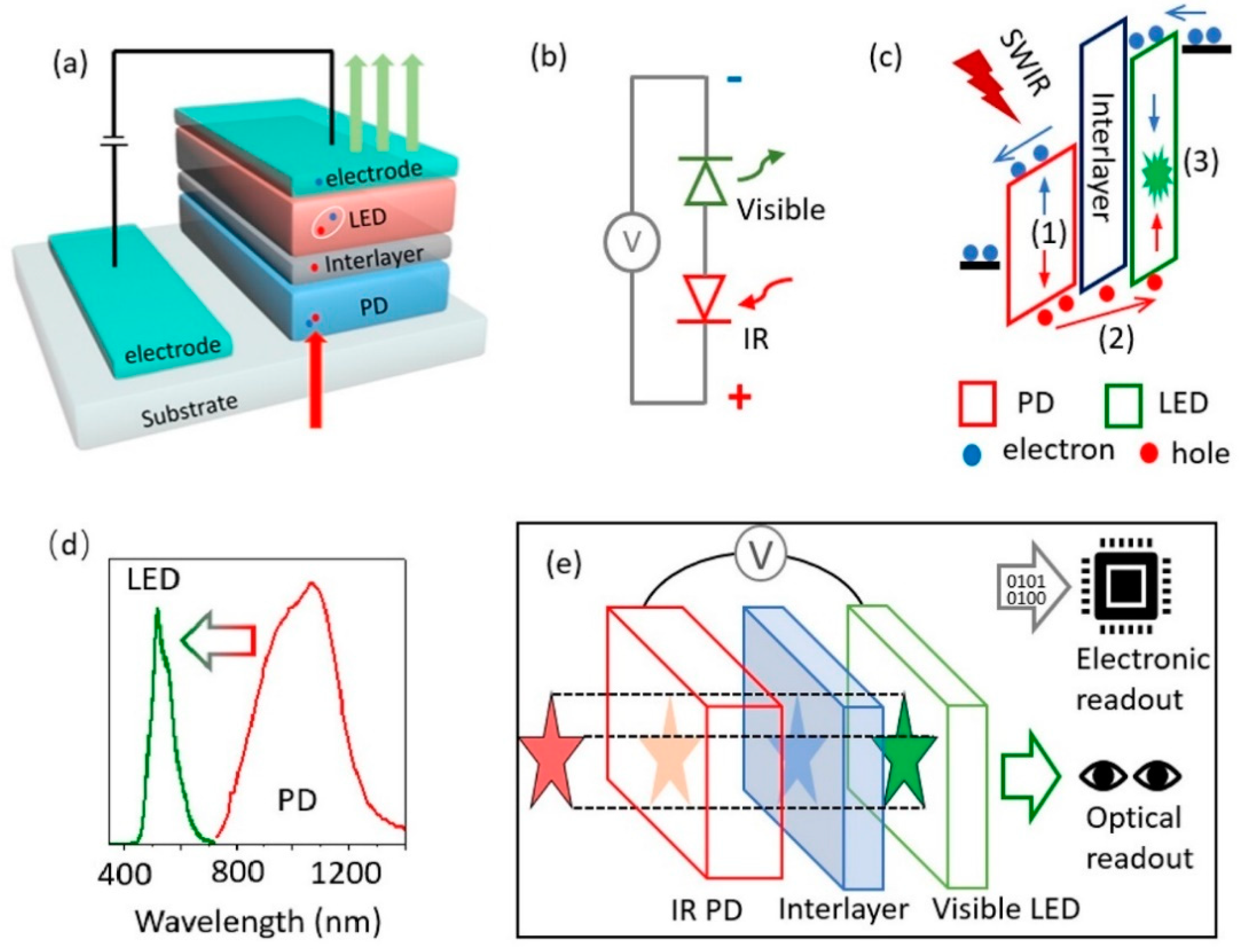
The upconversion device is integrated by infrared PD and LED in series, the structure is shown in Figure 2a. The OPD and OLED are arranged in a back-to-back configuration, the circuit model is illustrated in Figure 2b [23]. The visible OLED is forward biased while the infrared detector is reverse biased at the same time, which is designed to keep the OLED off in the darkness. The working principle of organic upconversion devices is shown in Figure 2c, when infrared light illuminates the PD, electron-hole pairs are generated. These excitons subsequently separate into free electrons and holes, and then the holes are transported to the emissive layer of the LED, while the electrons are extracted at the anode. The holes injected into the LED’s emissive layer recombine with electrons injected from the cathode, emitting visible photons and completing the upconversion from infrared to visible light. Additionally, the device provides electronic readout through photocurrent and optical readout through visible light, enabling high-resolution imaging [23]. In Figure 2d, the infrared light absorbed by the PD unit is upconverted to the visible-light emitting from the visible LED. When the upconversion device has completed the whole conversion process, the area illuminated by the infrared light will be displayed by the visible light emitted by the LED, as shown in Figure 2e.

2.2. Optoelectronic Characterization

Comprehensive optoelectronic characterization of organic upconversion devices is essential for enhancing their performance.
  • Absorption and Emission Spectra: The fundamental operation of organic upconversion devices hinges on their ability to absorb infrared photons and emit visible photons. The absorption spectrum of the device’s active layer is crucial as it dictates the range of IR wavelengths that the device can detect. Typically, organic upconversion imagers cover the NIR to shortwave infrared (SWIR) wavelengths, ranging from 800 to 1600 nm. This spectral response is primarily determined by the optical properties of the organic materials used in the photodetector layer [24]. The emission spectrum, on the other hand, is influenced by the materials used in the emitter layer. High purity in the electroluminescence spectrum is often achieved using materials such as perovskites and quantum dots, which can also be applied in upconversion imagers.
  • Quantum Efficiency and Upconversion Efficiency: Quantum efficiency is a vital metric for upconversion devices, encompassing both the external quantum efficiency (EQE) of the photodetector (EQE_det) and the emission layer (EQE_em). EQE_det refers to the efficiency with which absorbed NIR photons are converted into charge carriers, while EQE_em denotes the efficiency of converting these charge carriers into visible photons [25]. These efficiencies directly affect the overall performance and brightness of the upconversion device. Upconversion efficiency is a crucial parameter for evaluating the performance of upconversion devices, reflecting the effectiveness with which low-energy photons are converted into high-energy photons. Enhancing upconversion efficiency is essential for improving the practical applications of these devices. Upconversion efficiency (η) is typically defined as the ratio of the number of upconverted photons to the number of absorbed photons, expressed by the formula:
    η = N u m b e r o f u p c o n v e r t e d p h o t o n s N u m b e r o f a b s o r b e d p h o t o n s
  • Moreover, the upconversion efficiency of the devices depends on the responsivity of the PD and the external quantum efficiency of the LED. By optimizing the quantum efficiency, the upconversion efficiency and the overall performance of the upconversion equipment can be effectively improved [26,27].
  • Response Time and Bandwidth: The temporal response of upconversion devices is another critical parameter, especially for applications requiring real-time imaging. The response time is determined by the carrier transport properties within the organic layers. The response bandwidth, which represents the frequency range over which the device can operate effectively, is an important measure of the device’s speed. High-speed applications demand a broader bandwidth and faster response times [24].
  • Luminescence intensity: Luminescence intensity is a critical parameter in evaluating the optical performance of upconversion devices, reflecting the brightness of emitted light under excitation. It is influenced by factors such as material properties, excitation light intensity, doping concentration, and temperature. Higher luminescence intensity can be achieved by optimizing the upconversion materials’ energy level structures and quantum efficiencies, appropriate doping levels, and selecting suitable excitation wavelengths [28,29]. Measurement techniques, including steady-state spectroscopy, time-resolved spectroscopy, and photon counting, are employed to quantify luminescence intensity. Enhancements in luminescence intensity can be realized by material optimization, nanostructure design, surface modification, and excitation source optimization, ultimately improving the practical applications of upconversion devices in fields like bioimaging and sensing.
  • Detectivity: Detectivity (D*) reflects the ability of detectors to detect weak signals under a noisy background, especially for photodetectors [29,30]. Defined as
    D * = A Δ f N E P
    where A is the effective detector area, Δ f is the bandwidth, and NEP is the noise-equivalent power, higher D* values indicate greater sensitivity. D* is influenced by factors such as material properties, detector structure, operating temperature, and background noise. Enhancing D* involves optimizing upconversion materials for higher quantum efficiency, designing efficient detector structures, controlling operating temperatures to reduce thermal noise, and minimizing background noise.
  • Resolution: Resolution in upconversion devices, defined by the ability to distinguish fine details, is influenced by the morphology of the organic layers and the device architecture. Unlike traditional imagers that rely on pixel arrays, organic upconversion imagers are typically pixel-less. Thus, their resolution depends on the uniformity and smoothness of the multilayered films. Improving film morphology through advanced fabrication techniques such as thermal evaporation and solution processing can enhance resolution, potentially exceeding 1000 pixels per inch (PPI) [24].
The optoelectronic characterization of organic upconversion devices encompasses a range of parameters, including absorption and emission spectra, quantum efficiency, response time, noise characteristics, and resolution. Understanding and optimizing these parameters are crucial for advancing the performance and application scope of these devices. Continuous research and development in material science and fabrication technology are essential to overcome existing challenges and enhance the capabilities of organic upconversion devices.

3. Organic Infrared Photodetector

Organic infrared photodetectors have attracted considerable interest due to their advantageous properties such as flexibility, cost-effectiveness, and potential for large-area fabrication. These devices operate by converting infrared light into electrical signals through the use of organic materials. One critical aspect of organic infrared photodetectors is the incorporation of sensitizers, which are materials that absorb infrared photons and initiate the photodetection process. The performance of organic infrared photodetectors is heavily dependent on the choice and configuration of these sensitizers. Various sensitizer configurations have been explored to enhance device performance. In 2007, Lu et al. first utilized poly(N-vinylcarbazole) doped with an infrared photosensitizer, 2,4,7-trinitro-9-fluorenylidene malonitrile (TNFDM) as an infrared photosensitive material, realizing the optical upconversion of infrared light to visible light which confirmed the feasibility of all-organic NIR–visible light upconversion device [31].

3.1. BHJ Sensitizer

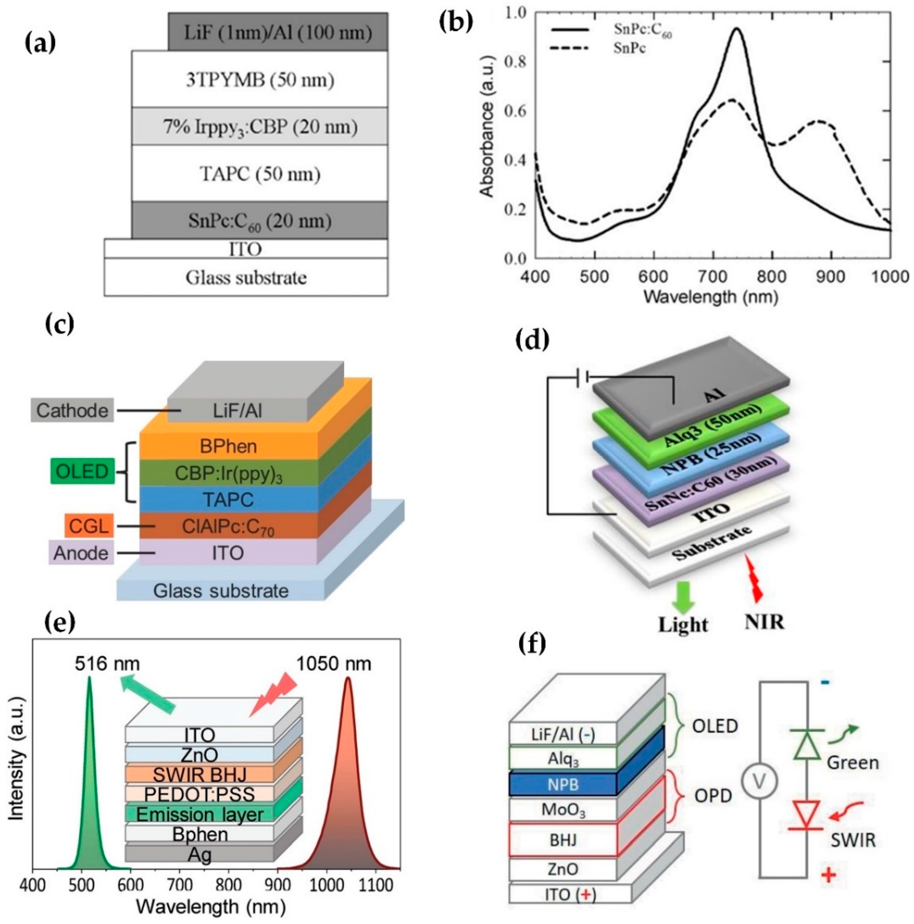
Bulk heterojunction (BHJ) sensitizers play a crucial role in the efficiency and performance of the OUDs. In 2010, Kim and his colleagues synthesized an upconversion device with a conversion efficiency of 2.7% by using a stannphthalocyanine (SnPc):C60 BHJ layer as a NIR sensitizer (Figure 3a) [32]. The absorption characteristics of SnPc:C60 are essential, especially its significant absorption in the NIR region, which extends up to 1000 nm. The absorption spectrum of SnPc films shows two distinct bands at 740 nm and 890 nm, while the SnPc:C60 mixed film exhibits a single peak at 740 nm (Figure 3b). The disappearance of the 890 nm peak in the mixed film is attributed to the suppression of dimer formation, which is beneficial for the performance of the device. This layer is characterized by strong IR absorption and low hole mobility, making it an ideal choice for upconversion devices. Under photovoltaic mode, the EQE of the SnPc:C60 bulk heterojunction device can be higher than 20% [33]. In their strategy for all-organic upconversion devices, they design a poor-hole-transport NIR-sensitizing layer to keep the OLEDs in the off state in the absence of IR irradiation, demonstrating superior performance.
In Shun-Wei Liu’s research [34,35], a blend of chloroaluminum phthalocyanine (ClAlPc) and C70 was utilized as a charge generation layer (CGL) and a phosphorescent OLED based on 4,4′-bis(N-carbazolyl)-1,1′-biphenyl (CBP) doped with fac-tris (2-phenylpyridine) iridium (III) [Ir(ppy)3] was used to emit green light. Upon optimizing the device structure (Figure 3c), the proposed transparent upconverter emitted a clear green spectrum under 780 nm NIR light, reaching a conversion efficiency of 6% at 7 V and exhibited high sensitivity to NIR illumination. Additionally, this research showcases three-dimensional imaging of real objects using a reflective and nonreflective object under NIR illumination in dark environments which emphasizes the high efficiency and potential utility of transparent organic upconversion devices in enhancing NIR sensing technologies [35,36].
Figure 3. Structure and performance characterization of the upconversion devices based on BHJ Sensitizers. (a) Schematic cross-section view of the IR-to-green-light upconversion device [32]. Copyright 2010, Advanced Materials. (b) Absorbance spectra of aSnPc film and SnPc:C60 mixed film [32]. Copyright 2010, Advanced Materials. (c) Device structure of the upconverter [35]. Copyright 2015, Advanced Materials. (d) Device structure of the up-converter [37]. Copyright 2017, Optical Materials. (e) The spectrum of a SWIR LED source used in the measurement and the EL spectrum of the SWIR-to-visible upconversion device in the presence of the SWIR (1050 nm) light illumination, the inset in (e): a schematic cross-sectional view of the SWIR visualizing device [38]. Copyright 2020, Advanced Science. (f) Material stacks and circuit model of the imager [24]. Copyright 2018, ACS Applied Electronic Materials.
Photonics 11 00808 g003
In addition, Tin (II) 2,3-naphthalocyanine (SnNc) alone or co-deposited with fullerenes SnNc:C60 can be used as organic NIR sensitive layers for the efficient upconversion devices together with a tris(8-hydroxyquinoline) aluminum(III) (Alq3) based OLEDs (Figure 3d) [37]. These devices offer significant advantages over conventional light converters, including lightweight, flexibility, low cost, and suitability for large-area applications. The unique optical and electronic properties of naphthalocyanines (Ncs), in comparison to phthalocyanines (Pcs), make them particularly attractive for optoelectronic applications [39,40,41]. In the research, the absorption spectrum of SnNc thin films revealed significant absorption around 875 nm, and NIR light at 830 nm was successfully upconverted, but the device showed a rather large dark luminance level because no hole blocking layer was used.
Li et al. reported their achievement of a SWIR visualization device that contains a large-area organic SWIR photodetector with sensitivity covering the wavelength range of 1000 to 1600 nm [38]. The organic SWIR photodetector is made from a blend of a near-infrared polymer diketopyrrolopyrroledithienylthieno [3,2-b]thiophene (DPP-DTT) and a non-fullerene n-type small molecule SWIR dye (Figure 3e). The integration of the organic SWIR photodetector with a perovskite LED achieved effective conversion of SWIR light to visible green light, demonstrating a photon-to-photon conversion efficiency of >0.1% under 14 V and offering a low-cost, solution-processable method for large-area SWIR detection and visualization.
In Li ‘s other study [23], SWIR imaging was realized by combining a SWIR organic photodiode (OPD) which absorbs light from 800 to 1400 nm, and a visible-light OLED based on Alq3 which emits visible light in the green spectrum region. The OPD and OLED layers are integrated into a back-to-back diode structure (Figure 3f), with the SWIR OPD reverse-biased and the OLED forward-biased. This design ensures efficient transport of photogenerated electrons and the emission of visible photons through electron-hole recombination. The OPD is a BHJ which consists of a SWIR-sensitive polymer and a fullerene derivative PC71BM [42,43]. The imager’s photoresponse performs well, achieving an EQE of 35% at low bias (≤3 V) and a 3 dB bandwidth of 10 kHz, with a large active area (2 cm2). In addition, the upconversion efficiency reaches 0.15% at a 3 V bias.

3.2. PHJ Sensitizer

BHJ sensitizers, which are widely used, also have some limitations. The upconversion device realized by BHJ sensitizers exhibited very poor performance because of the relatively large dark current density resulting from the poor electron-blocking efficiency of the BHJ layer. Therefore, Planar heterojunction (PHJ) sensitizers are also a good choice. PHJ configurations are widely used in organic photodetectors and organic photovoltaics (OPVs), especially in the NIR region [44,45].
A PHJ sensitizer typically involves a donor/acceptor(D/A) configuration that aids in the absorption and subsequent conversion of NIR light. In the research of Lv [46], lead phthalocyanine (PbPc)/C60 PHJ with a copper phthalocyanine (CuPc) template layer was used as an NIR sensitizer, the structure of the NIR-OPD is shown in Figure 4a. CuPc is used as a template layer to enhance the growth and crystallinity of PbPc, which improves its NIR absorption efficiency. When PHJ-based devices were combined with OLEDs, exhibiting improved performance metrics such as photosensitivity and photoresponsivity. This configuration mitigates issues like a dark current through the use of electron and hole-blocking layers, resulting in efficient NIR upconversion essential for advanced imaging technologies. Su et al. promoted the development of organic photodetectors (OPDs) with panchromatic photoresponse, capable of detecting light across a broad spectrum from ultraviolet (UV) to near-infrared (NIR) wavelengths [47]. They focus on two device structures: PHJ and hybrid planar-mixed molecular heterojunction (PM-HJ) (Figure 4b,c), utilizing PbPc as the donor and C70 fullerene as the acceptor due to their complementary absorption properties and efficient charge transport.

3.3. Organic Dyes Sensitizer

In 2018, Strassel and co-workers explored an alternative approach using an all-organic upconverter [48], which integrates NIR selective squaraine/fullerene dye-based organic photodetector with a fluorescent OLED to directly convert NIR light to visible light (see in Figure 4d) [49]. The organic photodetector, with peak sensitivity at 980 nm, was synthesized with a NIR-selective squaraine dye SQ-880/PC61BM blend and converts NIR photons into the electrical current with nearly 100% efficiency, which subsequently drives the OLED to emit visible light, effectively transforming the NIR image into the visible. The squaraine dye used in the OPD has been synthesized to extend the NIR response beyond 1100 nm, an improvement over previous devices that typically operated below this wavelength. The device which is made visibly transparent by being combined with an optimized semitransparent metal top electrode achieves an upconversion efficiency of 0.27% at 12 V and has an average visible transmittance of 65% and a peak transmittance of 80% at 620 nm. In 2019, they highlighted the use of a squaraine dye-based NIR photodetector paired with a fluorescent poly(para-phenylene vinylene) copolymer super yellow (SY)-based OLED, which efficiently converts NIR light (at around 980 nm) to visible yellow light with a conversion efficiency of 1.6% and a turn-on voltage in the range of 2.7–2.9 V. In addition, an electrolyte was added to the SY emitter, which transformed the OLED into a light-emitting electrochemical cell (LEC) [50]. The LEC variant shows dynamic behavior and can be stabilized under specific voltage conditions, offering a fault-tolerant processability from solution and a low driving voltage.
Hany and co-workers also investigated the performance of single-component layered squaraine dyes and their application in photodetectors which presents significant advancements in the development of organic materials for SWIR photodetection [25,51]. They demonstrated several SWIR squaraine dyes (such as benz[cd]indolium-capped squaraine dye, the corresponding dicyanomethylene acceptor-substituted dye, and the benz[cd]indol-flanked, rhodanine-substituted dye) which exhibit strong absorption in the SWIR range, with peak EQE exceeding 40% and detectable sensitivity at wavelengths up to 1300 nm. Moreover, the integration of these SWIR photodetectors with OLEDs led to the development of upconversion photodetectors (Figure 4e). The upconverter shows an efficient photon conversion of 1.85% from SWIR to visible green light, which offers a promising alternative to traditional inorganic-based imaging technologies, providing advantages such as flexibility, simpler processing, and potentially lower costs.
Figure 4. Structure and performance characterization of the upconversion devices. (a) The schematic structures of D/A PHJ NIR−OPD [46]. Copyright 2016, Organic Electronics. Structures of (b) PHJ OPD, (c) PM−HJ OPD [47]. Copyright 2015, ACS Applied Materials and Interfaces. (d) Architecture of the NIR OPD [48]. Copyright 2018, ACS Applied Materials and Interfaces. (e) Upconversion photodetector stack [51]. Copyright 2023, Advanced Optical Materials.
Photonics 11 00808 g004

4. Organic Light-Emitting Diode

4.1. Fluorescent OLED

Several organic upconversion devices are composed of an NIR organic photodetector and an OLED based on fluorescent materials. An OLED containing titanyl phthalocyanine (TiOPc) and Alq3 layers has been fabricated (Figure 5a) [52], which uses the TiOPc layer as a hole-producing layer rather than a traditional buffer layer, and the structure upconverted light at 650 nm to green light at 530 nm, indicating its potential in red to green light conversion. The thickness of the TiOPc layer has a significant impact on device performance, with specific thicknesses (e.g., 60 nm) providing the best results reducing the hole injection barrier and improving the hole injection efficiency, indicating that the TiOPc layer has to be designed with appropriate thickness to obtain the best performance. In the following study, the researchers constructed a photoresponsive OLED with the TiOPc layer acting as a photoconductive layer to realize the up-conversion of near-IR light to blue at the low drive voltage [53]. The OLED structure is composed of several layers which are constructed on top of the TiOPc layer, starting with a 200-nm-thick ITO-coated glass substrate. The blue-emitting diode includes N,N′-diphenyl-N,N′-bis(1-naphthyl)-1,1′-biphenyl-4,4′-diamine (α-NPD) as the hole transport and emitting layer, and 2,9-dimethyl-4,7-diphenyl-1,10-phenanthroline (bathocuproine or BCP) as the electron transport and hole blocking layer. The EL efficiency of the photoresponsive OLED is significantly enhanced under laser irradiation, with the device efficiency in the lower current density region surpassing that of an OLED without the TiOPc layer. Upon irradiation with NIR light, the device demonstrates blue emission at a lower drive voltage (between 5 and 12 V), indicating its function as a light switch and/or up-converter from NIR light (1.6 eV) to blue light (2.6 eV). The device shows an enhancement in blue emission with NIR light irradiation at higher voltages (above 12 V), achieving an ON/OFF ratio of up to 1000. The results indicate that this photoresponsive OLED is a promising candidate for IR-visible image conversion applications due to its ability to act as a light-switching device and up-converter at low drive voltages.
Recent studies have highlighted the importance of inverted OLEDs in improving the efficiency of organic NIR upconversion devices [44,46,54,55]. Lv et al. investigate the integration of inverted OLED structures with donor/acceptor PHJs to enhance the efficiency of NIR upconversion devices [46]. The inverted structure is designed with a bottom cathode, electron transport layer, light emission layer, hole transport layer, and top anode, making them compatible with existing n-type amorphous silicon thin-film transistor technology [56,57,58,59]. The inverted OLED comprised 2,9-dimethyl-4,7-diphenyl-1,10-phenanthroline (BCP), tris-(8-hydroxyquinoline) aluminum (Alq3), and 1,4-bis(1-naphthylphenylamino) biphenyl (NPB) for the electron transport, emitting, and hole transport layers. In their research, two configurations were explored: a photo-generated electron-based upconversion device with the inverted OLED on top of the D/A PHJ, and a photo-generated hole-based device with the D/A PHJ on top of the inverted OLED (Figure 5b). Both configurations demonstrated efficient upconversion performance, highlighting the potential of inverted OLED structures in future pixel-less NIR imaging applications.
Later, the inverted fluorescent OLED was integrated with PbPc:C60 BHJ sensitizer to realize upconversion [55]. Aim to enhance the photon-to-photon conversion efficiency by employing various device architectures and materials, they explore the impact of carrier blocking layers on device performance by inserting the MoO3 buffer layer, CuPc, and NPB EBL between the ITO cathode and the BHJ sensitizer [2,60]. The results show that devices incorporating CuPc as the electron blocking layer exhibit the highest performance due to CuPc’s high hole mobility, which improves carrier injection, recombination efficiency, and the performance of the devices.

4.2. Phosphorescent OLED

Phosphorescent OLEDs require a low current and voltage to emit light efficiently compared with fluorescent systems. An organic upconverter consisting of a tin phthalocyanine (SnPc):C60 bulk heterostructure layer with a fac-tris(2-phenylpyridinato)iridium (III) (Irppy3)-doped 4,4-N,N-dicarbazole-biphenyl (CBP) layer as a phosphorescent emitter, exhibiting superior current efficiency and the maximum photon-to-photon conversion efficiency reaches 2.7% at 15 V under IR irradiation [32].
The inverted OLED structure is also used in phosphorescent OLEDs. In Lv et al.’s research, they investigate the efficiency of NIR OUDs that utilize inverted phosphorescent OLEDs as emitters, a relatively underexplored area compared to devices with normal phosphorescent OLEDs. NIR OUDs created by simply integrating the NIR photosensitive layer and the inverted phosphorescent OLED active layer demonstrated a relatively low upconversion efficiency, which is primarily due to the high injection barrier for photo-generated electrons at the interface between the NIR photosensitive layer and the inverted OLED emitter [54]. The inverted structure, with the cathode at the bottom and the anode at the top, enhances stability by allowing the use of stable, transparent conductive oxide materials like ITO as the bottom cathode. The study compared the performance of three types of OUDs: those without a connecting layer (CL), with a Mg CL, and with a BCP:Li CL. The results indicated that devices without a CL or with a Mg CL had high electron injection barriers. Conversely, the introduction of a Li-doped BCP significantly reduced this barrier, facilitating better electron injection and thus higher upconversion efficiency. This was further validated through the fabrication and testing of inverted OLEDs, where the device with the Li-doped BCP:Li CL outperformed others, achieving a photon-to-photon conversion efficiency of 3.52%. OUDs with different CLs are shown in Figure 5c–e.

4.3. TADF OLED

Thermally activated delayed TADF OLEDs have gained significant attention in the development of organic upconversion devices due to their ability to convert NIR light into full-color visible light efficiently. The primary advantage of TADF materials lies in their small singlet-triplet energy gap ( EST), which facilitates efficient reverse intersystem crossing (RISC) from the triplet to the singlet state. This process enables the emission of delayed fluorescence and ensures that nearly all the electrogenerated excitons are utilized, leading to high internal electroluminescence (EL) quantum efficiency [61].
Recent research conducted by Adachi and co-workers has displayed great potential in producing high-efficiency OLEDs by utilizing the mechanism of TADF [62,63]. The TADF emitters were integrated into upconversion devices to convert NIR light to visible full-color light for the first time in Takuma Yasuda‘s research [64]. They incorporated TADF OLEDs with an organic BHJ CGL to accomplish a kind of innovative organic upconversion devices that exhibit NIR sensitivity up to 810 nm (Figure 6a). They utilized three representative TADF materials—4CzIPN (green emitter), 2CzPN (blue emitter), and 4CzTPN-Ph (red emitter), which were doped into host materials such as CBP (4,4′-bis(9-carbazolyl)-biphenyl) and mCP (1,3-bis(N-carbazolyl)benzene) to form the emission layer in a multilayer device structure [62], including a conductive oxide layer (ITO), a ZnO electron transport layer, a CGL, a HTL, an emission layer (TADF dopant + host material), an ETL, and an aluminum cathode. The upconversion devices demonstrate strong green, blue, and red TADF emissions with the highest external upconversion efficiencies of 0.11%, demonstrating their potential for various high-tech imaging applications.
Song et al. promoted the integration of a thermally activated delayed fluorescence (TADF) organic light-emitting diode (OLED) with a photomultiplying organic NIR photodetector (Figure 6b), which achieves a photon-to-photon upconversion efficiency can run up to 256% [65]. The TADF OLEDs, which utilize non-radiative triplet excitons for light emission through efficient reverse intersystem crossing via thermal activation, achieve high internal quantum efficiency (IQE) comparable to that of phosphorescent OLEDs without relying on precious metal complexes. Their work demonstrates an EQE of up to 20% using 2,5-bis(4-(10-phenoxazyl)phenyl)-1,3,4-oxadiazole (2PXZ-OXD) as the emission material, noted for its high photoluminescence quantum efficiency (PLQE) and suitability as a non-doped emission layer.
The TADF OLED in their work features an inverted photosensitization unit and a non-doped TADF OLED emission unit. It exhibits excellent performance metrics, including a low turn-on voltage of 2.4 V, a maximum luminance of 32,935 cd/m2, and a maximum EQE of 11.72%. Moreover, the integration with an organic NIR photodetector based on a PbPc/C60 PHJ enhances the upconversion efficiency by minimizing energy loss due to self-absorption and ensuring efficient charge carrier injection. The high efficiency and low cost of TADF OLEDs make them promising components for NIR-to-visible upconversion devices, with potential applications in night vision, biomedical imaging, and security. Therefore, the integration of TADF OLEDs into NIR-to-visible upconversion devices represents a significant advancement in the development of high-performance, all-organic upconversion displays.

4.4. Tandem OLED

Compared with traditional single-layer structures where only one type of photocarrier is used for current-to-light conversion, tandem organic upconverters show higher efficiency and better performance for their use of both two carriers. Tandem OLEDs incorporate a double-layer structure whose configuration consists of two phosphorescent OLED layers separated by a CGL that effectively absorbs NIR photons and generates electron-hole pairs. These carriers are subsequently injected into the respective OLED layers, where recombination occurs. The tandem structure allows each NIR photon to induce light emission in both OLED layers, including the recombination of photoelectrons with holes in the first OLED and the recombination of photoholes with electrons in the second OLED, which significantly enhances the overall light conversion efficiency. In 2018, the researchers introduced a novel tandem OLED structure to enhance the efficiency of NIR to visible light conversion [66,67]. For the overall structure, this innovative device consists of a SnNcCl2:C60 sensitive layer and OLEDs. For the OLED part, a CBP: Ir(ppy)3 layer was used as phosphorescent emission layer (EML), an NPB layer was used as a hole transport layer (HTL), and a B4PyPPM layer was used as an electron transport layer (ETL). What’s more, they add an ultrathin intermediate connecting layer (ICL) of Liq/Al to promote the photoelectron injection into the first OLED (Figure 6c,d) [68]. In their result, the tandem device shows a maximum photon-to-photon conversion efficiency of 4.8% at 25.6 V, which is nearly equivalent to the theoretical maximum. Additionally, this design effectively suppresses leakage current, improving the ON/OFF switching ratio [66].
Figure 6. Structure and performance characterization of the upconversion devices. (a) Schematic cross–sectional view of organic NIR–to–visible upconversion devices based on TADF–OLEDs and chemical structures of the representative organic semiconductor materials used in the devices [64]. Copyright 2017, ACS Photonics. (b) Structure of the upconversion device [65]. Copyright 2018, The Journal of Physical Chemistry Letters. Schematic structure diagrams of (c) a conventional organic upconversion device with one OLED unit and (d) a tandem organic upconversion device with two OLED units [66]. Copyright 2018, Applied Physics Letters. (e) Structure and working mechanism of the upconversion device under dark (top image) and illumination conditions (lower image) [69]. Copyright 2018, Materials Horizons.
Photonics 11 00808 g006
Taking a step forward, another tandem organic upconverter has been fabricated to improve the performance of the devices, which was combined by a broadband photodetector based on PDPP3T as a donor with a tandem phosphorescent OLED (Figure 6e) [69,70,71]. The tandem OLED emits the same green light as the normal OLED but the turn-on voltage for the tandem OLED reaches 5.2 V, approximately double that of the single-unit OLED (2.7 V). The tandem OLED exhibits significantly enhanced performance, achieving an efficiency of 191.5 cd/A and an EQE of 50%. These values are 2.23 times greater than those of the single-unit devices, which record 85.5 cd/A and 22.5% EQE. At an equivalent current density, the tandem OLED’s brightness is double that of the single-unit OLED. Additionally, the maximum power efficiency for both devices is comparable, approximately 100 lm/W [72,73]. Moreover, in their work, they reached a photon-to-photon conversion efficiency of 29.6% at 12 V, one of the highest reported values, which was attributed to the two light-emitting layers and the photomultiplication effect by visible emitted light, resulting in additional electron-hole pairs and reducing the visible light loss absorbed by the photodetector.
In summary, various types of organic upconversion devices have demonstrated significant potential in the fields of photodetection and imaging. Compared to traditional inorganic materials, organic upconversion devices offer advantages such as low cost, flexibility, and simple fabrication processes. The innovations of the devices not only address many limitations of traditional devices but also pave the way for future high-performance optoelectronic applications. The performance of the organic upconversion devices discussed above is shown in Table 1.

5. Applications

Upconversion devices show great potential in a number of applications ranging from bioimaging, medical applications, and imaging through smog and silicon wafers thanks to its many advantages. These devices offer enhanced performance in low-light conditions, enabling the detection and conversion of IR photons into visible light with high efficiency. This capability makes them particularly valuable for applications in imaging, sensing, and display technologies. Additionally, the ability to tune the emission wavelength through material and structural modifications allows for versatile and customizable solutions. Their high sensitivity, combined with low energy consumption and the potential for integration into flexible substrates, positions upconversion devices as promising components for advanced optoelectronic systems and emerging technologies and highlights the versatility and effectiveness of upconversion devices in advancing various fields of science and technology.
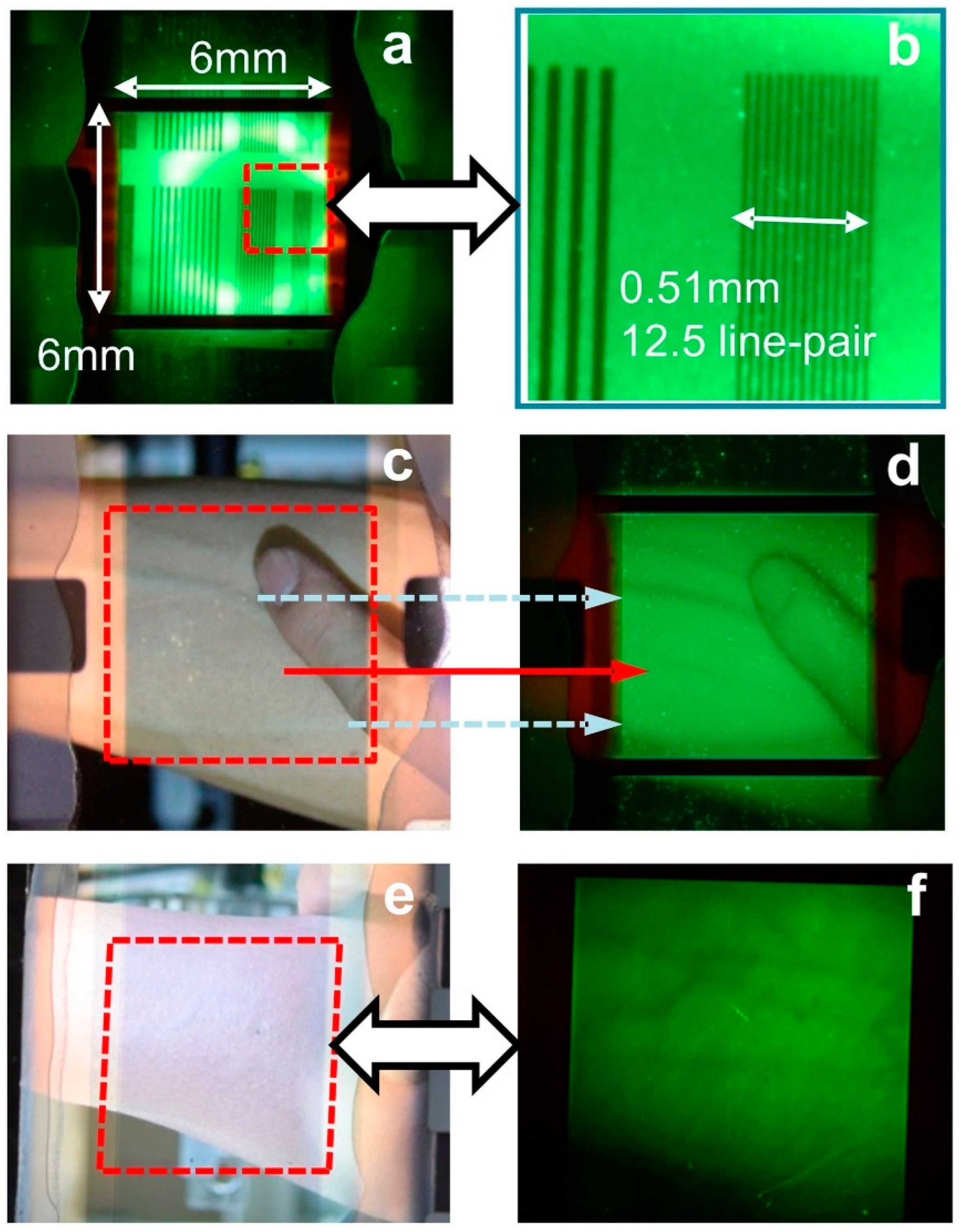
Shun-Wei Liu et al. describe a 3.46% conversion efficiency, cathodic-controlled, and NIR organic upconverter for local blood vessel mapping [68]. The device comprises transparent electrodes (Ag/MoO3) and a large active area (6 mm × 6 mm), operating by applying a constant voltage of 5 V and using a 780 nm NIR LED for illumination. NIR light penetrates several millimeters of human skin, particularly blood vessels, due to the high absorption of NIR light by blood. The line-shaped shadow mask was clearly presented when illuminated by a 780-nm NIR LED in the dark. Figure 7a shows a magnified view of the region marked by a dashed square, and the line-pairs were distinctly visible in Figure 7b. Based on previous research, the device achieved high-resolution imaging at 600 dpi [35]. Figure 7c,e illustrates a forearm viewed through the transparent upconverter under normal room lighting. When near-infrared light is used in a dark environment, the green image on the upconverter allows for the clear identification of veins beneath the skin, as depicted in Figure 7d,f. Remarkably, the system accurately identifies the contours of blood vessels even on darker skin (Figure 7e), as shown in Figure 7f, which demonstrates the applicability of the transparent organic upconverter as an NIR imaging device for local blood vessels.
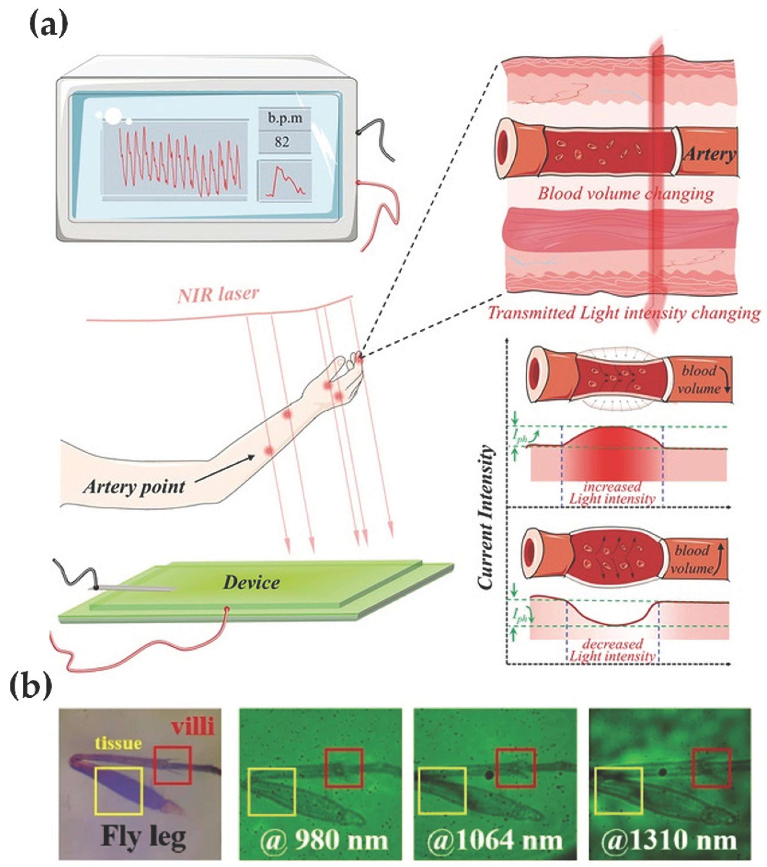
He et al. reported the application of near-infrared organic photodetectors in advanced biomedical scenarios [74]. NIR-OPDs have been successfully employed for high-quality artery monitoring using a transmission-type method (see Figure 8a) and the NIR-OPD enabled the successful imaging of squamous metaplasia in the cervix and carcinoma in the large intestine. These results underline the potential of NIR-OPDs in providing noninvasive, direct imaging methods that offer crucial diagnostic information, representing significant advancements in biomedical technology, and positioning NIR-OPDs as valuable tools for clinical diagnosis and health monitoring.
Zhang et al. reported the imaging of the villi on a fly’s leg under NIR light (Figure 8b) [30], demonstrating the OUCs’ capability to capture detailed images of biological samples under NIR illumination. The researchers used a biological slide sample of a fly leg for their experiments. The visible light image obtained by a CCD camera showed identifiable villi on the fly’s leg, but the internal tissue details were barely detectable, presenting only an outline. However, when using the UCD under different wavelengths of NIR illumination, the images showed a distinct outline of the sample. Particularly, under 980 nm illumination, the image of the villi was clear, and the internal tissue also exhibited high image quality. Furthermore, due to the deeper penetration of 1310 nm NIR light, it could easily penetrate the thicker shell of the sample, revealing more detailed structures. This indicates the importance of long wavelengths for non-invasive bio-imaging applications. The study concluded that the UCD exhibited high efficiency and a long wavelength response, making it a promising tool for non-invasive bio-imaging, capable of providing clear visual images from 850 to 1310 nm.
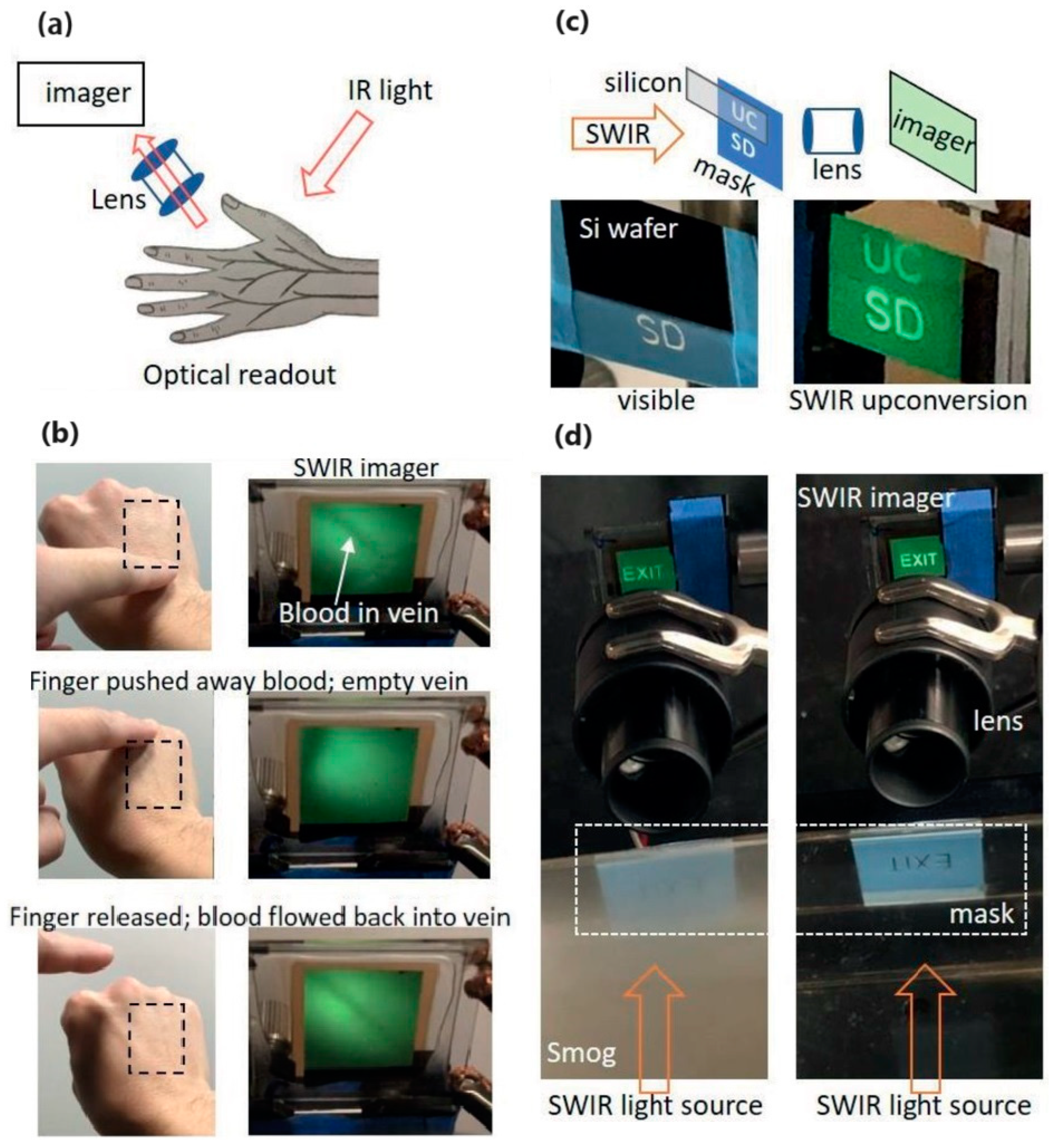
Li presents an organic upconversion imager with dual electronic and optical readout capabilities, capable of simultaneously recording vascular positions and blood flow pulses [23]. This imager provides a non-invasive method to visualize vascular structures and blood flow in real-time by converting SWIR light into visible light (shown in Figure 9a). This functionality is particularly valuable for medical diagnostics and continuous health monitoring, as it enables healthcare professionals to directly observe blood flow while also providing quantitative data through electronic readouts for automated analysis and long-term monitoring, thereby enhancing the precision and efficiency of medical procedures. Figure 9b shows a motion sequence of manipulating blood flow, as one pressed down on a vein to push away blood and then released the pressure to let blood flow back into the vein [23]. Moreover, the upconversion imager was also utilized for inspection or environmental monitoring with SWIR light. As shown in Figure 9c, the SWIR imager can clearly display the mask pattern (letter “UC”) covered by silicon wafers. Figure 9d demonstrates the effect of smog on visible and SWIR imaging. In the presence of smog, it’s difficult to identify the letters (EXIT) on the mask for the scatter of the visible light. However, SWIR light can penetrate the smog and be clearly presented by the upconversion imager.
In the work of Mu and co-workers, they reported their achievement of an intelligent interactive optoelectronic device that can realize infrared, temperature sensing, and multicolor visualization display by integrating a multi-stimuli responsive silicon (Si) sensor and a color-tunable OLED (CTOLED) [75]. The CTOLEDs developed are particularly significant because of their ability to dynamically switch colors in response to different stimuli, a feature that is leveraged to create interactive multi-signal visualization systems. This innovation is achieved through the precise control of the emission spectra of the OLEDs, which allows for the fine-tuning of color outputs corresponding to specific signals. The displays can visually differentiate between multiple signals by shifting the emitted color, which is particularly useful in complex environments where simultaneous monitoring of various parameters is required. Applications highlighted in the research include intelligent sensor systems, where the CTOLEDs can be used for real-time data visualization, offering immediate and intuitive feedback to users. The ability to interact with and visualize data in this manner opens up new possibilities in fields such as environmental monitoring, healthcare diagnostics, and advanced human-machine interfaces. The research underscores the potential of CTOLEDs in enhancing the functionality of smart devices and expanding the capabilities of optoelectronic technologies in multi-signal processing and visualization.
The tunability of the multicolor OLED is achieved through the careful selection of organic materials and device architecture, which enables the OLED to shift its emission from one color to another. They demonstrate that by modulating the driving conditions of the OLED (Figure 10a), different colors can be emitted from a single device, providing a flexible platform for multicolor displays. Integrating the multicolor OLED with the infrared sensor Si, the Si/CTOLED device realizes to convert the invisible infrared to visible light (Figure 10b). These interactive displays are designed to respond to IR light by altering their color output, thereby making invisible IR signals visible to the human eye through color changes. By providing a visual representation of IR signals, these interactive displays enable users to intuitively monitor and respond to environmental changes that are typically outside the visible spectrum. Different intensities of infrared light cause the Si sensor to generate different amounts of current, which causes the tunable multicolor OLED to emit different visible colors. The photos of Si/CTOLED devices at different infrared intensities are shown in Figure 10c. In addition, they proposed a wearable temperature visualization monitor due to the ability to sense the temperature of Si. This monitor leverages the color-tunable properties of the OLEDs to provide a visual representation of temperature changes. In this wearable device, the OLED display changes color in response to the wearer’s body temperature, allowing for real-time monitoring (Figure 10d). The color shift occurs due to the interaction between the temperature sensor and the OLED’s emission properties, which are finely tuned to respond to temperature variations. This capability is particularly useful in medical and fitness applications, where continuous and immediate feedback on body temperature is crucial. As shown in Figure 10d, the device is flexible and suitable to wear.
Shun-Wei Liu and co-workers also demonstrated the semi-transparent, pixel-free upconversion goggles with dual audio-visual communication (shown in Figure 11a) [76], which represents a significant advancement in wearable infrared imaging technology. These goggles are designed to integrate infrared visualization into wearable electronics, offering a novel solution for applications requiring both visual and audio communication. A distinguishing feature of these goggles is their ability to synchronize audio signal transmission with the light source, facilitating concurrent delivery of both audio and visual information, which enhances the functionality of the goggles, making them highly suitable for environments where integrated communication is essential. The goggles are capable of high-resolution infrared imaging and utilize large-area, semi-transparent OUDs to convert invisible infrared images into the visible spectrum. With an optimized device structure, these goggles achieve more than 30% efficiency in converting infrared photons to visible light, facilitated by the use of chloroaluminum phthalocyanine (ClAlPc) as the charge generation layer, which ensures effective charge dissociation and prolonged carrier lifetime. The potential applications of these goggles are vast, including night vision, security and surveillance, search and rescue operations, medical diagnostics, and industrial inspection. In night vision and security contexts, the goggles provide clear visual information in low-light conditions and can detect infrared signals in complete darkness, respectively, enhancing monitoring capabilities. In search and rescue scenarios, they enable the detection of individuals in low-visibility environments, while in medical diagnostics, they can identify infrared signatures indicative of various conditions. Additionally, in industrial settings, the goggles facilitate the inspection of machinery and infrastructure by detecting infrared emissions due to heat or other factors, with real-time audio-visual communication ensuring timely maintenance and repairs. Figure 11b shows the infrared images processed by the see-through upconversion goggles. Overall, these innovative goggles combine efficient infrared-to-visible upconversion with dual communication functionalities, making them a versatile tool for enhancing safety and efficiency across multiple fields.
In facial recognition systems, capturing clear images under low-light or dark conditions is challenging. Traditional systems rely on visible light, which limits their effectiveness in such environments. Shun-Wei Liu describes how single-pixel, large-area upconversion panels can address this limitation by converting invisible infrared light into visible light [77], which allows the facial recognition system to capture clear images of faces even in low-light conditions, significantly improving the accuracy and reliability of the recognition process and making it more versatile for real-world applications. The ability to unveil invisible infrared light of the facial recognition technology is shown in Figure 11c. In addition, they highlight that the single-pixel, large-area upconversion panels can convert the weak infrared signals into visible light, thereby enhancing the sensitivity and precision of light detection and ranging (LiDAR) systems. This conversion enables LiDAR to function effectively even in environments with poor ambient light, ensuring accurate distance measurements and high-resolution mapping and opening up new possibilities for their deployment in various fields requiring precise spatial information. The demonstration of light detection ranging from the single-pixel, large-area upconversion panel is shown in Figure 11d.

6. Challenges and Outlook

Although there has been considerable progress in the upconversion devices in recent years, some issues and limitations still require further research.
Upconversion efficiency and Stability: Although upconversion efficiency in imagers, particularly those operating in the longer infrared wavelengths, shows potential, it remains suboptimal. This inefficiency is primarily attributed to the scarcity of high-performance organic infrared materials and a limited understanding of device physics. One viable approach to enhance the efficiency of PDs and LEDs is by introducing photomultiplication mechanisms into the PDs and employing out-coupling structures in the LEDs. However, these techniques may complicate the device architecture and increase costs [24]. Organic materials often suffer from lower quantum yields compared to their inorganic counterparts, and their stability can be compromised under prolonged exposure to light and environmental conditions. Enhancing the photostability and quantum efficiency of organic upconversion materials remains a critical area of research. In practical applications, background IR light from the environment can interfere with the detection of upconverted visible light. This background noise can mask the weak signals produced by the upconversion process, reducing the signal-to-noise ratio. Implementing effective background subtraction techniques and enhancing the sensitivity of detection systems are necessary to address this challenge.
Spectral Overlap and Broad Emission Bands: Organic upconversion materials often exhibit broad emission spectra, which can lead to spectral overlap. This overlap complicates the precise detection and differentiation of specific wavelengths, especially when multiple emission peaks are present. Designing materials with narrower emission bands or implementing filtering techniques can help mitigate this issue [78].
Material Design and Synthesis: Designing and synthesizing organic materials with optimal properties for upconversion is complex. It requires a deep understanding of molecular interactions, energy transfer mechanisms, and the ability to precisely control the photophysical properties through chemical modifications [79]. The development of multifunctional devices that combine upconversion with other functionalities, such as sensing, photodetection, and energy harvesting, holds great promise. Such devices could open up new applications in medical diagnostics, environmental monitoring, and smart textiles.
Integrating OUDs with existing imaging, photovoltaic, and display technologies requires compatibility in terms of materials, device architectures, and operational conditions. Ensuring seamless integration while maintaining the unique advantages of organic upconversion materials poses a significant challenge. Nevertheless, the infrared-to-visible upconversion technique is gaining increasing attention due to its ease of fabrication and potential for high resolution.
Wavelength Detection: The current upconversion devices are mainly concentrated in the NIR band, and the research on SWIR and above-infrared upconversion devices is much less. This disparity in research focus is primarily due to the challenges associated with efficient photon conversion in the SWIR and mid-infrared (MIR) regions. The lower energy of photons in these bands necessitates the use of materials with smaller energy gaps, which often suffer from reduced photostability and lower quantum efficiencies. Additionally, the development of suitable sensitizers and acceptors for SWIR and MIR upconversion is still in its infancy, with few materials demonstrating the requisite properties for efficient upconversion.
Recent efforts have aimed at identifying new organic compounds and hybrid materials that can operate effectively in these longer wavelength regions. For instance, the design of novel organic-inorganic hybrid structures has shown potential in extending the operational wavelength range of upconversion devices. Furthermore, advancements in nanotechnology and material science are paving the way for the development of more robust and efficient upconversion systems capable of working in the SWIR and MIR bands. Addressing these challenges will be crucial for expanding the applicability of upconversion technologies to new areas such as telecommunications, medical imaging, and environmental monitoring.
Stability and Longevity: Stability remains a critical issue for the practical application of OUDs. Organic materials are prone to degradation under prolonged exposure to light and oxygen, leading to a reduction in device performance over time. Strategies to enhance stability include encapsulation techniques, the development of more robust organic materials, and the incorporation of protective layers that prevent oxygen and moisture ingress. For instance, encapsulating OUDs in inert matrices such as polymers or glass has been shown to significantly extend their operational lifetime [80].
Low-dimensional materials: Such as quantum dots, two-dimensional (2D) materials, and nanowires, have shown significant potential in the field of upconversion devices and open new avenues for enhancing the performance of OUDs [81,82,83]. These materials exhibit unique physical and chemical properties that can be leveraged to address some of the limitations inherent in traditional bulk materials.
High-quality quantum structures, advanced epitaxial technologies, and characterization methods are essential to drive the development of infrared optoelectronic materials and devices [84]. An atomic imaging technique was used to observe and analyze the atomic arrangement within the superlattice. Moreover, the researchers provide detailed descriptions of the lattice structure and atomic-scale features, identifying the degree of intermixing at the interfaces between the different materials and investigating the structural and optical properties of a type II superlattice composed of alternating layers of InAs and In0.5Ga0.5As0.5Sb0.5, which exhibited high radiation recombination efficiency in the long-wave infrared band and longer minority carrier lifetime.
Impurity doping not only provides a fundamental approach to impart unique electronic, magnetic, and optical properties to target nanomaterials but also has a critical influence on nucleation and growth of many functional nanocrystals [85]. The study reveals that the upconversion luminescence efficiency and emission intensity are strongly affected by the doping process. Enhanced upconversion luminescence is observed in nanocrystals with optimized doping concentrations which indicates that precise control over doping can improve the luminescence performance of these materials. In addition, the findings demonstrate the potential of doping as a tool to tailor the optical properties of upconversion nanocrystals. The ability to control the morphology, crystal structure, and upconversion luminescence properties through doping provides valuable insights for the design of advanced materials for applications in bioimaging, sensing, and light-emitting devices.

7. Conclusions

In this review, we reviewed the development of the OUDs in recent years. OUDs represent an innovative photonic technology with significant potential for converting low-energy photons into high-energy photons, which have developed rapidly as a result of the advances of organic materials and the progress of synthesis technology. Although OUDs face challenges in terms of efficiency and stability, material design and synthesis, device fabrication, scalability and cost, and integration with existing technologies, ongoing research and innovation are continually overcoming these obstacles. Advances in material science, improved fabrication techniques, the development of multifunctional devices, interdisciplinary collaborative research, and the push toward commercialization provide a broad scope for the future development of OUDs. In conclusion, the research on organic upconversion devices is rapidly progressing, and as the technology continues to mature and advance, OUDs are expected to bring revolutionary changes to various technological fields. Through sustained innovation and collaboration, the performance of OUDs will continually improve, and their application areas will expand, contributing significantly to the advancement of modern technology.

Funding

G.M. is sponsored by National Natural Science Foundation of China (NSFC No. 62305022). X.T. is sponsored by National Key R&D Program of China (2021YFA0717600), National Natural Science Foundation of China (NSFC No. 62035004, NSFC No. U22A2081), and Young Elite Scientists Sponsorship Program by CAST (No. YESS20200163).

Institutional Review Board Statement

Not applicable.

Informed Consent Statement

Not applicable.

Data Availability Statement

Not applicable.

Conflicts of Interest

The authors declare no conflicts of interest.

References

  1. Armin, A.; Jansen-van Vuuren, R.D.; Kopidakis, N.; Burn, P.L.; Meredith, P. Narrowband light detection via internal quantum efficiency manipulation of organic photodiodes. Nat. Commun. 2015, 6, 6343. [Google Scholar] [CrossRef] [PubMed]
  2. Baeg, K.J.; Binda, M.; Natali, D.; Caironi, M.; Noh, Y.Y. Organic Light Detectors: Photodiodes and Phototransistors. Adv. Mater. 2013, 25, 4267–4295. [Google Scholar] [CrossRef] [PubMed]
  3. Siegmund, B.; Mischok, A.; Benduhn, J.; Zeika, O.; Ullbrich, S.; Nehm, F.; Böhm, M.; Spoltore, D.; Fröb, H.; Körner, C.; et al. Organic narrowband near-infrared photodetectors based on intermolecular charge-transfer absorption. Nat. Commun. 2017, 8, 15421. [Google Scholar] [CrossRef]
  4. García de Arquer, F.P.; Armin, A.; Meredith, P.; Sargent, E.H. Solution-processed semiconductors for next-generation photodetectors. Nat. Rev. Mater. 2017, 2, 16100. [Google Scholar] [CrossRef]
  5. Kang, D.; Jeon, E.; Kim, S.; Lee, J. Lanthanide-Doped Upconversion Nanomaterials: Recent Advances and Applications. BioChip J. 2020, 14, 124–135. [Google Scholar] [CrossRef]
  6. Dubey, N.; Chandra, S. Miniaturized Biosensors Based on Lanthanide-Doped Upconversion Polymeric Nanofibers. Biosensors 2024, 14, 116. [Google Scholar] [CrossRef] [PubMed]
  7. Wieghold, S.; Bieber, A.S.; Lackner, J.; Nienhaus, K.; Nienhaus, G.U.; Nienhaus, L. One-Step Fabrication of Perovskite-Based Upconversion Devices. ChemPhotoChem 2020, 4, 704–712. [Google Scholar] [CrossRef]
  8. Mehrdel, B.; Nikbakht, A.; Aziz, A.A.; Jameel, M.S.; Dheyab, M.A.; Khaniabadi, P.M. Upconversion lanthanide nanomaterials: Basics introduction, synthesis approaches, mechanism and application in photodetector and photovoltaic devices. Nanotechnology 2021, 33, 082001. [Google Scholar] [CrossRef]
  9. Liu, H.; Gao, M.; Poole, P.J.E.L. 1.5 µm up-conversion device. Electron. Lett. 2000, 36, 1300–1301. [Google Scholar] [CrossRef]
  10. Chen, J.; Ban, D.; Helander, M.G.; Lu, Z.H.; Poole, P. Near-Infrared Inorganic/Organic Optical Upconverter with an External Power Efficiency of >100%. Adv. Mater. 2010, 22, 4900–4904. [Google Scholar] [CrossRef]
  11. Ban, D.; Han, S.; Lu, Z.H.; Oogarah, T.; SpringThorpe, A.J.; Liu, H.C. Near-infrared to visible light optical upconversion by direct tandem integration of organic light-emitting diode and inorganic photodetector. Appl. Phys. Lett. 2007, 90, 093108. [Google Scholar] [CrossRef]
  12. Shang, Y.; Hao, S.; Yang, C.; Chen, G. Enhancing Solar Cell Efficiency Using Photon Upconversion Materials. Nanomaterials 2015, 5, 1782–1809. [Google Scholar] [CrossRef] [PubMed]
  13. Safdar, M.; Ghazy, A.; Lastusaari, M.; Karppinen, M. Lanthanide-based inorganic–organic hybrid materials for photon-upconversion. J. Mater. Chem. C 2020, 8, 6946–6965. [Google Scholar] [CrossRef]
  14. Yin, H.-J.; Xiao, Z.-G.; Feng, Y.; Yao, C.-J. Recent Progress in Photonic Upconversion Materials for Organic Lanthanide Complexes. Materials 2023, 16, 5642. [Google Scholar] [CrossRef]
  15. Liang, G.; Wang, H.; Shi, H.; Wang, H.; Zhu, M.; Jing, A.; Li, J.; Li, G. Recent progress in the development of upconversion nanomaterials in bioimaging and disease treatment. J. Nanobiotechnol. 2020, 18, 154. [Google Scholar] [CrossRef]
  16. Hu, Y.; Chen, L.; Li, H.; Jiang, H.; Wang, K.; Li, N.; Zhang, Q.; Lei, Y. Decoupling the Trade-Off Between the Photosignal and Photonoise in Upconversion Devices Through a Solution-Processed Nickel Oxide Interconnecting Layer. Adv. Opt. Mater. 2023, 12, 2302021. [Google Scholar] [CrossRef]
  17. Zhang, N.; Tang, H.; Shi, K.; Wang, W.; Deng, W.; Xu, B.; Wang, K.; Sun, X.W. High-performance all-solution-processed quantum dot near-infrared-to-visible upconversion devices for harvesting photogenerated electrons. Appl. Phys. Lett. 2019, 115, 221103. [Google Scholar] [CrossRef]
  18. Dong, S.; Zhang, Y.; Wang, Z.; Li, J.; Zhou, Z.; Zhu, L.; Zhong, H.; Liu, F.; Jiang, X. Solution-Processed Efficient Organic Upconversion Device for Direct NIR Imaging. Adv. Opt. Mater. 2024, 12, 2400912. [Google Scholar] [CrossRef]
  19. Liu, P.; Guo, L.; Qi, F.; Li, W.; Li, W.; Fu, Q.; Yao, J.; Xia, M.; Liu, Z.; Wang, Y. Large dynamic range and wideband mid-infrared upconversion detection with BaGa4Se7 crystal. Optica 2022, 9, 50–55. [Google Scholar] [CrossRef]
  20. Fang, J.; Wang, Y.; Yan, M.; Wu, E.; Huang, K.; Zeng, H. Highly Sensitive Detection of Infrared Photons by Nondegenerate Two-Photon Absorption Under Midinfrared Pumping. Phys. Rev. Appl. 2020, 14, 064035. [Google Scholar] [CrossRef]
  21. Fu, Q.; Liu, P.; Li, W.; Qi, F.; Pang, Z.; Li, W.; Wang, Y.; Liu, Z. High-Resolution and Wide-Span Terahertz Frequency Measurement Using Nonlinear Up-Conversion. IEEE Trans. Instrum. Meas. 2024, 73, 1005307. [Google Scholar] [CrossRef]
  22. Zhao, J.; Xu, K.; Yang, W.; Wang, Z.; Zhong, F. The triplet excited state of Bodipy: Formation, modulation and application. Chem. Soc. Rev. 2015, 44, 8904–8939. [Google Scholar] [CrossRef] [PubMed]
  23. Li, N.; Eedugurala, N.; Leem, D.S.; Azoulay, J.D.; Ng, T.N. Organic Upconversion Imager with Dual Electronic and Optical Readouts for Shortwave Infrared Light Detection. Adv. Funct. Mater. 2021, 31, 2100565. [Google Scholar] [CrossRef]
  24. Hu, X.; Xiao, G.; Li, Y.; Wu, S.-E.; Chen, Q.; Li, N.; Sui, X. Infrared-Light Visualization by Organic Upconversion Devices. ACS Appl. Electron. Mater. 2023, 5, 5378–5385. [Google Scholar] [CrossRef]
  25. Hany, R.; Cremona, M.; Strassel, K. Recent advances with optical upconverters made from all-organic and hybrid materials. Sci. Technol. Adv. Mater. 2019, 20, 497–510. [Google Scholar] [CrossRef]
  26. Wu, D.; Guo, J.; Du, J.; Xia, C.; Zeng, L.; Tian, Y.; Shi, Z.; Tian, Y.; Li, X.J.; Tsang, Y.H. Highly polarization-sensitive, broadband, self-powered photodetector based on graphene/PdSe2/germanium heterojunction. ACS Nano 2019, 13, 9907–9917. [Google Scholar] [CrossRef]
  27. Wu, D.; Guo, C.; Zeng, L.; Ren, X.; Shi, Z.; Wen, L.; Chen, Q.; Zhang, M.; Li, X.J.; Shan, C.-X.; et al. Phase-controlled van der Waals growth of wafer-scale 2D MoTe2 layers for integrated high-sensitivity broadband infrared photodetection. Light Sci. Appl. 2023, 12, 5. [Google Scholar] [CrossRef]
  28. Yang, Y.; Zhu, Y.; Zhou, J.; Wang, F.; Qiu, J. Integrated strategy for high luminescence intensity of upconversion nanocrystals. ACS Photonics 2017, 4, 1930–1936. [Google Scholar] [CrossRef]
  29. Dibaba, S.T.; Ge, X.; Ren, W.; Sun, L. Recent progress of energy transfer and luminescence intensity boosting mechanism in Nd3+-sensitized upconversion nanoparticles. J. Rare Earths 2019, 37, 791–805. [Google Scholar] [CrossRef]
  30. Zhang, Y.; He, Z.; Du, X.; Han, J.; Lin, H.; Zheng, C.; Wang, J.; Yang, G.; Tao, S. High-performance organic upconversion device with 12% photon to photon conversion efficiency at 980 nm and bio-imaging application in near-infrared region. Opt. Express 2022, 30, 16644–16654. [Google Scholar] [CrossRef]
  31. Lu, J.; Zheng, Y.; Chen, Z.; Xiao, L.; Gong, Q. Optical upconversion devices based on photosensitizer-doped organic light-emitting diodes. Appl. Phys. Lett. 2007, 91, 201107. [Google Scholar] [CrossRef]
  32. Kim, D.Y.; Song, D.W.; Chopra, N.; De Somer, P.; So, F. Organic Infrared Upconversion Device. Adv. Mater. 2010, 22, 2260–2263. [Google Scholar] [CrossRef] [PubMed]
  33. Kim, D.Y.; Sarasqueta, G.; So, F. SnPc:C60 bulk heterojunction organic photovoltaic cells with MoO3 interlayer. Sol. Energy Mater. Sol. Cells 2009, 93, 1452–1456. [Google Scholar] [CrossRef]
  34. Shih, C.-J.; Li, Y.-Z.; Li, M.-Z.; Biring, S.; Huang, B.-C.; Liu, C.-W.; Yeh, T.-H.; Luo, D.; Lee, J.-H.; Huang, Y.-H.; et al. Transparent organic upconversion device targeting high- grade infrared visual image. Nano Energy 2021, 86, 106043. [Google Scholar] [CrossRef]
  35. Liu, S.W.; Lee, C.C.; Yuan, C.H.; Su, W.C.; Lin, S.Y.; Chang, W.C.; Huang, B.Y.; Lin, C.F.; Lee, Y.Z.; Su, T.H. Transparent Organic Upconversion Devices for Near-Infrared Sensing. Adv. Mater. 2015, 27, 1217–1222. [Google Scholar] [CrossRef] [PubMed]
  36. Liu, S.-W.; Li, Y.-Z.; Lin, S.-Y.; Li, Y.-H.; Lee, C.-C. Inducing the trap-site in an emitting-layer for an organic upconversion device exhibiting high current-gain ratio and low turn-on voltage. Org. Electron. 2016, 30, 275–280. [Google Scholar] [CrossRef]
  37. Melquíades, M.C.; Aderne, R.; Cuin, A.; Quirino, W.G.; Cremona, M.; Legnani, C. Investigation of Tin(II)2,3-naphtalocyanine molecule used as near-infrared sensitive layer in organic up-conversion devices. Opt. Mater. 2017, 69, 54–60. [Google Scholar] [CrossRef]
  38. Li, N.; Lan, Z.; Lau, Y.S.; Xie, J.; Zhao, D.; Zhu, F. SWIR Photodetection and Visualization Realized by Incorporating an Organic SWIR Sensitive Bulk Heterojunction. Adv. Sci. 2020, 7, 2000444. [Google Scholar] [CrossRef]
  39. El-Khouly, M.E.; Gutiérrez, A.M.; Sastre-Santos, Á.; Fernández-Lázaro, F.; Fukuzumi, S. Light harvesting zinc naphthalocyanine–perylenediimide supramolecular dyads: Long-lived charge-separated states in nonpolar media. Phys. Chem. Chem. Phys. 2012, 14, 3612. [Google Scholar] [CrossRef]
  40. Pham, T.A.; Song, F.; Stöhr, M. Supramolecular self-assembly of metal-free naphthalocyanine on Au(111). Phys. Chem. Chem. Phys. 2014, 16, 8881. [Google Scholar] [CrossRef]
  41. Pandey, R.; Kerner, R.A.; Menke, S.M.; Holst, J.; Josyula, K.V.B.; Holmes, R.J. Tin naphthalocyanine complexes for infrared absorption in organic photovoltaic cells. Org. Electron. 2013, 14, 804–808. [Google Scholar] [CrossRef]
  42. Karuthedath, S.; Firdaus, Y.; Liang, R.Z.; Gorenflot, J.; Beaujuge, P.M.; Anthopoulos, T.D.; Laquai, F. Impact of fullerene on the photophysics of ternary small molecule organic solar cells. Adv. Energy Mater. 2019, 9, 1901443. [Google Scholar] [CrossRef]
  43. Li, N.; Lim, J.; Azoulay, J.D.; Ng, T.N. Tuning the charge blocking layer to enhance photomultiplication in organic shortwave infrared photodetectors. J. Mater. Chem. C 2020, 8, 15142–15149. [Google Scholar] [CrossRef]
  44. Li, N.; Li, T.; Li, L.S.; Li, J. Efficient and Stable OLEDs with Inverted Device Structure Utilizing Solution-Processed ZnO-Based Electron Injection Layer. Adv. Opt. Mater. 2023, 11, 2300467. [Google Scholar] [CrossRef]
  45. Wang, X.; Li, H.; Su, Z.; Fang, F.; Zhang, G.; Wang, J.; Chu, B.; Fang, X.; Wei, Z.; Li, B.; et al. Efficient organic near-infrared photodetectors based on lead phthalocyanine/C60 heterojunction. Org. Electron. 2014, 15, 2367–2371. [Google Scholar] [CrossRef]
  46. Lv, W.; Zhong, J.; Peng, Y.; Li, Y.; Luo, X.; Sun, L.; Zhao, F.; Zhang, J.; Xia, H.; Tang, Y.; et al. Organic near-infrared upconversion devices: Design principles and operation mechanisms. Org. Electron. 2016, 31, 258–265. [Google Scholar] [CrossRef]
  47. Su, Z.; Hou, F.; Wang, X.; Gao, Y.; Jin, F.; Zhang, G.; Li, Y.; Zhang, L.; Chu, B.; Li, W. High-Performance Organic Small-Molecule Panchromatic Photodetectors. ACS Appl. Mater. Interfaces 2015, 7, 2529–2534. [Google Scholar] [CrossRef] [PubMed]
  48. Strassel, K.; Kaiser, A.; Jenatsch, S.; Véron, A.C.; Anantharaman, S.B.; Hack, E.; Diethelm, M.; Nüesch, F.; Aderne, R.; Legnani, C.; et al. Squaraine Dye for a Visibly Transparent All-Organic Optical Upconversion Device with Sensitivity at 1000 nm. ACS Appl. Mater. Interfaces 2018, 10, 11063–11069. [Google Scholar] [CrossRef] [PubMed]
  49. Chen, G.; Sasabe, H.; Igarashi, T.; Hong, Z.; Kido, J. Squaraine dyes for organic photovoltaic cells. J. Mater. Chem. A 2015, 3, 14517–14534. [Google Scholar] [CrossRef]
  50. Strassel, K.; Ramanandan, S.P.; Abdolhosseinzadeh, S.; Diethelm, M.; Nüesch, F.; Hany, R. Solution-Processed Organic Optical Upconversion Device. ACS Appl. Mater. Interfaces 2019, 11, 23428–23435. [Google Scholar] [CrossRef]
  51. Hu, W.H.; Nüesch, F.; Giavazzi, D.; Jafarpour, M.; Hany, R.; Bauer, M. Squaraine Dyes for Single-Component Shortwave Infrared-Sensitive Photodiodes and Upconversion Photodetectors. Adv. Opt. Mater. 2023, 12, 2302105. [Google Scholar] [CrossRef]
  52. Ni, J.; Tano, T.; Ichino, Y.; Hanada, T.; Kamata, T.; Takada, N.; Yase, K. Organic Light-Emitting Diode with TiOPc Layer–A New Multifunctional Optoelectronic Device. Jpn. J. Appl. Phys. 2001, 40, L948. [Google Scholar] [CrossRef]
  53. Chikamatsu, M.; Ichino, Y.; Takada, N.; Yoshida, M.; Kamata, T.; Yase, K. Light up-conversion from near-infrared to blue using a photoresponsive organic light-emitting device. Appl. Phys. Lett. 2002, 81, 769–771. [Google Scholar] [CrossRef]
  54. Lv, W.; Zheng, H.; Li, X.; Lu, F.; Xu, S.; Sun, L.; Peng, Y. Enhancing Upconversion Efficiency of Organic Near Infrared Upconversion Devices Based on Inverted Phosphorescent OLEDs as Emitters by Introducing Connecting Layer. IEEE Trans. Electron Devices 2024, 71, 2165–2170. [Google Scholar] [CrossRef]
  55. Lv, W.; Zhou, J.; Zhou, Z.; Li, X.; Dai, Q.; Xu, S.; Zhong, J.; Liang, Y.; Sun, L.; Lu, F.; et al. An investigation of design principles toward near infrared organic upconversion devices. Opt. Mater. 2021, 121, 111487. [Google Scholar] [CrossRef]
  56. Zhou, X.; Pfeiffer, M.; Huang, J.S.; Blochwitz-Nimoth, J.; Qin, D.S.; Werner, A.; Drechsel, J.; Maennig, B.; Leo, K. Low-voltage inverted transparent vacuum deposited organic light-emitting diodes using electrical doping. Appl. Phys. Lett. 2002, 81, 922–924. [Google Scholar] [CrossRef]
  57. Park, C.H.; Lee, H.J.; Hwang, J.H.; Kim, K.N.; Shim, Y.S.; Jung, S.-G.; Park, C.H.; Park, Y.W.; Ju, B.-K. High-Performance Hybrid Buffer Layer Using 1,4,5,8,9,11-Hexaazatriphenylenehexacarbonitrile/Molybdenum Oxide in Inverted Top-Emitting Organic Light-Emitting Diodes. ACS Appl. Mater. Interfaces 2015, 7, 6047–6053. [Google Scholar] [CrossRef]
  58. Lee, H.; Kang, C.-M.; Park, M.; Kwak, J.; Lee, C. Improved efficiency of inverted organic light-emitting diodes using tin dioxide nanoparticles as an electron injection layer. ACS Appl. Mater. Interfaces 2013, 5, 1977–1981. [Google Scholar] [CrossRef]
  59. Knauer, K.A.; Najafabadi, E.; Haske, W.; Gaj, M.P.; Davis, K.C.; Fuentes-Hernandez, C.; Carrasco, U.; Kippelen, B. Stacked inverted top-emitting green electrophosphorescent organic light-emitting diodes on glass and flexible glass substrates. Org. Electron. 2013, 14, 2418–2423. [Google Scholar] [CrossRef]
  60. Chen, X.; Xu, Z.; Peng, Y.; Lv, W.; Ding, R.; Xu, S.; Sun, L. Enhanced performance of near infrared and broad spectral response organic photodiodes exploiting NPB as electron blocking layer. Infrared Phys. Technol. 2019, 102, 103001. [Google Scholar] [CrossRef]
  61. Adachi, C.; Baldo, M.A.; Thompson, M.E.; Forrest, S.R. Nearly 100% internal phosphorescence efficiency in an organic light-emitting device. J. Appl. Phys. 2001, 90, 5048–5051. [Google Scholar] [CrossRef]
  62. Uoyama, H.; Goushi, K.; Shizu, K.; Nomura, H.; Adachi, C. Highly efficient organic light-emitting diodes from delayed fluorescence. Nature 2012, 492, 234–238. [Google Scholar] [CrossRef] [PubMed]
  63. Tao, Y.; Yuan, K.; Chen, T.; Xu, P.; Li, H.; Chen, R.; Zheng, C.; Zhang, L.; Huang, W. Thermally Activated Delayed Fluorescence Materials towards the Breakthrough of Organoelectronics. Adv. Mater. 2014, 26, 7931–7958. [Google Scholar] [CrossRef] [PubMed]
  64. Tachibana, H.; Aizawa, N.; Hidaka, Y.; Yasuda, T. Tunable Full-Color Electroluminescence from All-Organic Optical Upconversion Devices by Near-Infrared Sensing. ACS Photonics 2017, 4, 223–227. [Google Scholar] [CrossRef]
  65. Song, Q.; Lin, T.; Su, Z.; Chu, B.; Yang, H.; Li, W.; Lee, C.-S. Organic Upconversion Display with an over 100% Photon-to-photon Upconversion Efficiency and a Simple Pixelless Device Structure. J. Phys. Chem. Lett. 2018, 9, 6818–6824. [Google Scholar] [CrossRef]
  66. He, S.-J.; Wang, D.-K.; Yang, Z.-X.; Man, J.-X.; Lu, Z.-H. Integrated tandem device with photoactive layer for near-infrared to visible upconversion imaging. Appl. Phys. Lett. 2018, 112, 243301. [Google Scholar] [CrossRef]
  67. He, S.J.; Wang, D.K.; Jiang, N.; Tse, J.S.; Lu, Z.H. Tunable Excitonic Processes at Organic Heterojunctions. Adv. Mater. 2015, 28, 649–654. [Google Scholar] [CrossRef]
  68. Yuan, C.-H.; Lee, C.-C.; Liu, C.-F.; Lin, Y.-H.; Su, W.-C.; Lin, S.-Y.; Chen, K.-T.; Li, Y.-D.; Chang, W.-C.; Li, Y.-Z.; et al. Cathodic-controlled and near-infrared organic upconverter for local blood vessels mapping. Sci. Rep. 2016, 6, 32324. [Google Scholar] [CrossRef]
  69. Yang, D.; Zhou, X.; Ma, D.; Vadim, A.; Ahamad, T.; Alshehri, S.M. Near infrared to visible light organic up-conversion devices with photon-to-photon conversion efficiency approaching 30%. Mater. Horiz. 2018, 5, 874–882. [Google Scholar] [CrossRef]
  70. Yang, D.; Zhou, X.; Wang, Y.; Vadim, A.; Alshehri, S.M.; Ahamad, T.; Ma, D. Deep ultraviolet-to-NIR broad spectral response organic photodetectors with large gain. J. Mater. Chem. C 2016, 4, 2160–2164. [Google Scholar] [CrossRef]
  71. Zhou, X.; Yang, D.; Ma, D. Extremely Low Dark Current, High Responsivity, All-Polymer Photodetectors with Spectral Response from 300 nm to 1000 nm. Adv. Opt. Mater. 2015, 3, 1570–1576. [Google Scholar] [CrossRef]
  72. Sun, H.; Guo, Q.; Yang, D.; Chen, Y.; Chen, J.; Ma, D. Corrections to High Efficiency Tandem Organic Light Emitting Diode Using Organic Heterojunction as Charge Generation Layer: An Investigation into Charge Generation Model and Device Performance. ACS Photonics 2015, 2, 668. [Google Scholar] [CrossRef]
  73. Sun, H.; Chen, Y.; Zhu, L.; Guo, Q.; Yang, D.; Chen, J.; Ma, D. Realization of Optimal Interconnector for Tandem Organic Light-Emitting Diodes with Record Efficiency. Adv. Electron. Mater. 2015, 1, 1500176. [Google Scholar] [CrossRef]
  74. He, Z.; Du, X.; Zheng, C.; Yu, X.; Lin, H.; Tao, S. High-Quality Artery Monitoring and Pathology Imaging Achieved by High-Performance Synchronous Electrical and Optical Output of Near-Infrared Organic Photodetector. Adv. Sci. 2022, 10, 2203870. [Google Scholar] [CrossRef]
  75. Mu, G.; Rao, T.; Qi, Y.; Ma, S.; Hao, Q.; Chen, M.; Tang, X. Color-Tunable Organic Light-Emitting Displays for Interactive Multi-Signal Visualization. Adv. Funct. Mater. 2023, 33, 2301280. [Google Scholar] [CrossRef]
  76. Shih, C.J.; Lin, C.Y.; Chen, K.; Amin, N.R.A.; Luo, D.; Hsu, I.S.; Akbar, A.K.; Biring, S.; Lu, C.H.; Chen, B.H.; et al. Semi-Transparent, Pixel-Free Upconversion Goggles with Dual Audio-Visual Communication. Adv. Sci. 2023, 10, 232631. [Google Scholar] [CrossRef]
  77. Shih, C.-J.; Huang, Y.-C.; Wang, T.-Y.; Yu, C.-W.; Hsu, I.-S.; Akbar, A.K.; Lin, J.-Y.; Biring, S.; Lee, J.-H.; Liu, S.-W. Transparent organic upconversion devices displaying high-resolution, single-pixel, low-power infrared images perceived by human vision. Sci. Adv. 2023, 9, eadd7526. [Google Scholar] [CrossRef]
  78. Hu, W.H.; Vael, C.; Diethelm, M.; Strassel, K.; Anantharaman, S.B.; Aribia, A.; Cremona, M.; Jenatsch, S.; Nüesch, F.; Hany, R. On the Response Speed of Narrowband Organic Optical Upconversion Devices. Adv. Opt. Mater. 2022, 10, 2200695. [Google Scholar] [CrossRef]
  79. Huang, Z.; Miyashita, T.; Tang, M.L. Photon Upconversion at Organic-Inorganic Interfaces. Annu. Rev. Phys. Chem. 2024, 75, 329–346. [Google Scholar] [CrossRef]
  80. Ren, P.; Zheng, X.; Zhang, J.; De Camillis, S.; Jia, J.; Wang, H.; Liao, X.; Piper, J.A.; Lu, Y. Quantifying the influence of inert shell coating on luminescence brightness of lanthanide upconversion nanoparticles. ACS Photonics 2022, 9, 758–764. [Google Scholar] [CrossRef]
  81. Ma, S.; Wei, H.; Zhu, H.; Ling, F.C.-C.; Wang, X.; Su, S. Higher-Order Multiphoton Absorption Upconversion Lasing Based on ZnO/ZnMgO Multiple Quantum Wells. Nanomaterials 2022, 12, 3073. [Google Scholar] [CrossRef] [PubMed]
  82. Wang, Q.; Wee, A.T. Photoluminescence upconversion of 2D materials and applications. J. Phys. Condens. Matter. 2021, 33, 223001. [Google Scholar] [CrossRef]
  83. Rao, T.; Chen, M.; Mu, G.; Tang, X. Infrared-to-Visible Upconversion Devices. Coatings 2022, 12, 456. [Google Scholar] [CrossRef]
  84. Shi, C.; Wang, D.; Li, W.; Fang, X.; Zhang, B.; Wang, D.; Hao, Y.; Fang, D.; Zhao, H.; Du, P.; et al. Atomic imaging and optical properties of InAs/In0.5Ga0.5As0.5Sb0.5 type II superlattice. Appl. Phys. Lett. 2024, 124, 251101. [Google Scholar] [CrossRef]
  85. Liu, M.-M.; Zheng, G.-C.; Wei, Y.; Tian, D.; Zheng, Q.-B.; Huang, L.; Xie, J. Doping induced morphology, crystal structure, and upconversion luminescence evolution: From Na3ScF6:Yb/Er/Y to NaYF4:Yb/Er/Sc nanocrystals. Rare Met. 2022, 42, 1018–1027. [Google Scholar] [CrossRef]
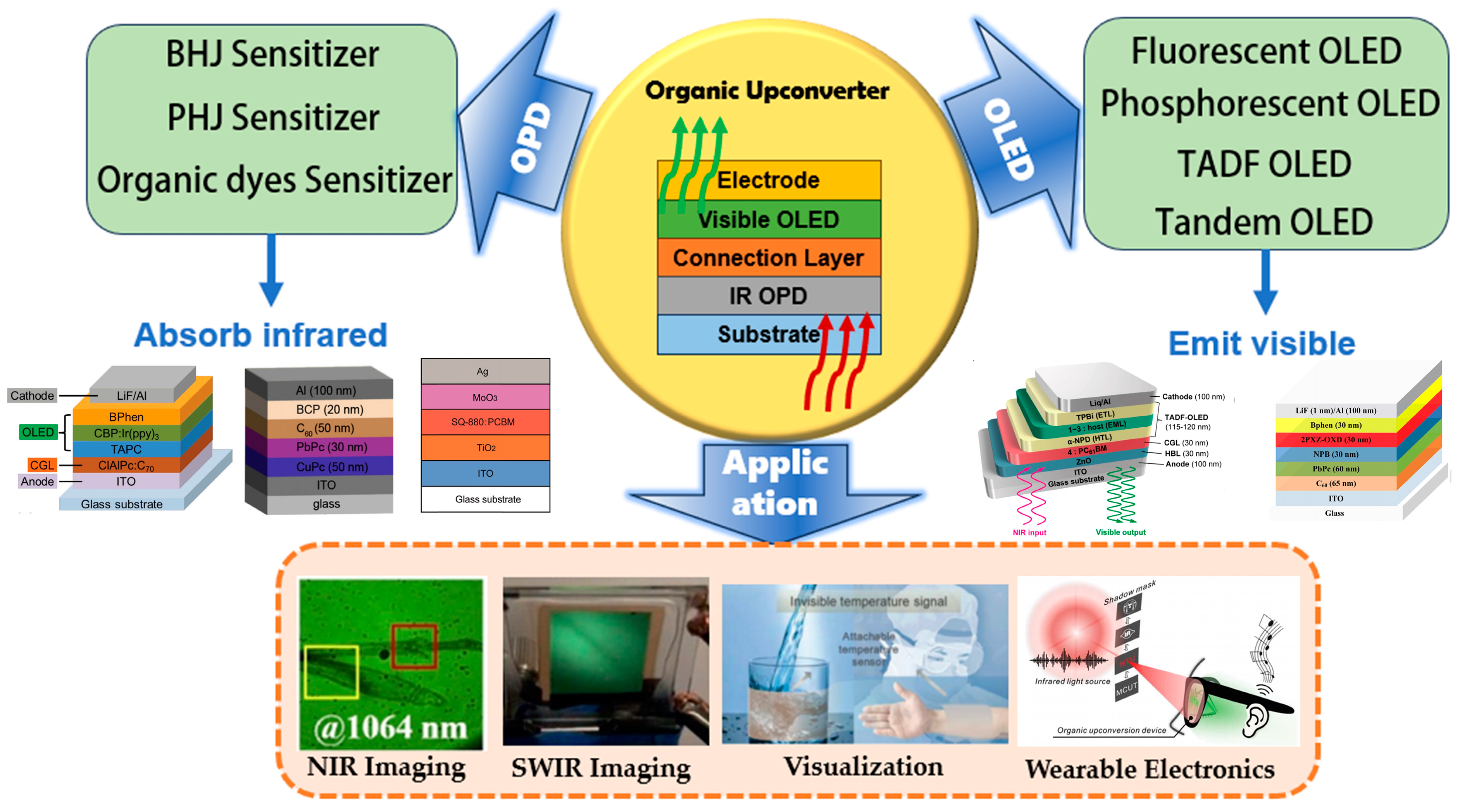
Figure 1. Schematic of advances in organic upconversion devices.
Photonics 11 00808 g001
Figure 2. Structure and operation principles for upconversion imagers [24]. Copyright 2018, ACS Applied Electronic Materials (a) Schematic diagram of an upconversion device. (b) Equivalent circuit and (c) working principle for the upconversion imager. (d) Example of the response spectrum for PD and the electroluminance spectrum for LED in an upconversion device. (e) Imaging process for an upconversion imager.
Photonics 11 00808 g002
Figure 5. Structure and performance characterization of the upconversion devices. (a) Schematic cross-section of the device [52]. Copyright 2001, Japanese Journal of Applied Physics. (b) Two types of upconversion devices [46]. Copyright 2016, Organic Electronics. Schematic of OUDs (c) without CL, (d) with Mg CL, and (e) with BCP:Li CL [54]. Copyright 2024, IEEE Transactions on Electron Devices.
Photonics 11 00808 g005
Figure 7. NIR upconverter for local blood vessel mapping application [68]. Copyright 2016, Scientific Reports. (a) Real converted image of the line-shaped shadow mask captured by the transparent upconverter under NIR illumination. (b) Zoom-in image from the area marked by the dash square in (a). (c) Observing human forearm through the transparent upconverter. The solid arrows represent specific blood vessels in the human forearm, and the dashed arrow denotes an obscure blood vessel located deeper below the skin. (d) Converted NIR image captured by the transparent upconverter in the darkness. (e) Human forearm shows an inconspicuous vein shape. (f) Converted NIR image shows vein position with a dark brown color captured by the transparent upconverter in a dark environment.
Photonics 11 00808 g007
Figure 8. Imaging demonstrations using upconversion imagers. (a) Test schematic diagram of transmissive type artery pulse monitoring in real time [74]. Copyright 2022, Advanced Science. (b) The biological sample images of fly legs under CCD and UCD [30]. Copyright 2022, Optics Express.
Photonics 11 00808 g008
Figure 9. Imaging of the dual-readout imager [23]. Copyright 2021, Advanced Functional Materials. (a) The reflected IR light from a human hand was upconverted by the imager. (b) Imaging blood flow in a vein. The dashed box indicates the area being imaged. (c) Imaging of an object behind a silicon wafer. (d) Comparison of imaging through a smog chamber.
Photonics 11 00808 g009
Figure 10. Interactive Multi-Signal Visualization [75]. Copyright 2023, Advanced Functional Materials. (a) Photographs of the multicolor OLED at different applied voltages. (b) The structure chart of the Si/CTOLED device. (c) Photographs of the Si/CTOLED device under different infrared intensities. (d) Conceptual diagram of wearable temperature visualization monitor.
Photonics 11 00808 g010
Figure 11. (a) Wireless dual-mode operation of the OUDs (b) Photograph of the infrared images processed by the upconversion goggles [76]. Copyright 2023, Advanced Science. (c) Infrared visualization of the facial recognition technology by the wearable, semitransparent, large-area, and single-pixel upconversion panel. (d) Infrared visualization of the LiDAR function by the upconversion panel [77]. Copyright 2023, Science Advances.
Photonics 11 00808 g011
Table 1. Progress in organic upconversion devices.
YearInfrared
Material
OLED
Material
Active Area
(cm2)
Detect
Range (nm)
EmissionMaximum
Brightness
(cd/m2)
Conversion
Efficiency
Ref.
2007PVK:TNFDMAlq3-810Green
(530 nm)
--[31]
2010SnPc:C60CBP: Ir(ppy)30.04~830Green853
at 15 V
2.7%
at 15 V
[32]
2015ClAlPc:C70CBP: Ir(ppy)30.04
or 0.16
~780Green1553
at 7 V
6%
at 7 V
[35]
2016PbPc: C60Alq30.16
or 0.5
900Green-0.043%
at 28 V
[46]
2017SnPc:C60Alq30.03~875Green6182
at 12 V
0.45%
at 13 V
[37]
2017ING-T-DPP:
PC61BM
4CzIPN:2CzPN
:4CzTPN-Ph
4~810Full-color-0.11
at 10 V
[64]
2018PbPc: C602PXZ-OXD2 × 2808~900Green32,935
at 9.5 V
256%
at 15 V
[65]
2018PDPP3T-PCBMBe(pp)2:
Ir(ppy)2(acac)
0.16
or 4
~850Green1504
at 12 V
29.6%
at 12 V
[69]
2018SQ-880: PCBMAlq31.6~1000Green313
at 12 V
0.27%
at 12 V
[48]
2019SQ-880: PCBMSY0.03
or 0.07
~980Yellow760
at 7.5 V
1.6%
at 12 V
[18]
2020DPP–DTT: IR dyeCsPbBr31.0 × 1.51000~1600
(peak:1050)
Green
(516 nm)
-0.1%
at 14 V
[38]
2021SWIR-sensitive polymer: PC71BMAlq30.1
or 2
800~1400Green-0.15%
at 3 V
[23]
2023DCSQ1: PCBMCzDBA1.0 × 1.51300Greenish-yellow
(575 nm)
20
at 2 V
1.85%
at 10 V
[51]
Disclaimer/Publisher’s Note: The statements, opinions and data contained in all publications are solely those of the individual author(s) and contributor(s) and not of MDPI and/or the editor(s). MDPI and/or the editor(s) disclaim responsibility for any injury to people or property resulting from any ideas, methods, instructions or products referred to in the content.