Article

Comparative Analysis of Free-Running and Gating Imaging Modes of SPAD Sensors

School of Electronic Science and Engineering, Nanjing University, Nanjing 210000, China
*
Author to whom correspondence should be addressed.
Photonics 2024, 11(8), 721; https://doi.org/10.3390/photonics11080721
Submission received: 29 June 2024 / Revised: 23 July 2024 / Accepted: 29 July 2024 / Published: 31 July 2024

Abstract

:
A single-photon avalanche diode (SPAD) is a photon-counting sensor renowned for its exceptional single-photon sensitivity. One significant feature of SPADs is their non-linear response to light, making them ideal for high-dynamic range imaging applications. In SPAD imaging, the photon detection mode, which depends on the quenching method employed, is crucial for optimizing image quality and dynamic range. This paper examines the free-running and gating imaging modes, evaluating their impacts on photon capture and saturation limits. Given that the number of incident photons follows a Poisson distribution, we introduce an innovative imaging-quenching model based on statistical mathematics. We designed and fabricated two SPAD imaging sensors using 180 nm CMOS technology. Image processing and evaluation were conducted using a mapping method. Our results show that in low-light conditions, the gating mode surpasses the free-running mode in the signal-to-noise ratio (SNR). However, the free-running mode exhibits a saturation limit of more than an order of magnitude higher than that of the gating mode, demonstrating its superior capability to handle a broader range of light intensities. This paper provides a thorough analysis of the differences between the two imaging methods, incorporating the theoretical mathematical model, circuit characteristics, and computed imaging quality.

1. Introduction

Due to their exceptional time resolution and digital signal processing capabilities, SPADs have been extensively applied in various fields, including positron emission tomography [1], quantum random number generation [2,3], LiDAR systems [4,5], and fluorescence lifetime imaging [6,7,8]. In recent years, significant advancements in image sensor technology have been observed, transitioning from the popular CCD sensors of 20 years ago to the prevalent CMOS image sensors (CIS) used today. Compared to traditional cameras, SPADs typically have larger pixels and a higher tendency for dark current [9]. However, advances in tape-out processes and 3D stacking technologies [9] have improved the fill factor of SPADs, making them suitable for mobile devices. These enhancements enable photon counting at higher frequencies and ultra-high resolution within a single frame. SPADs’ high time resolution allows them to function in both 2D and 3D imaging modes [10]. In 3D imaging, SPADs are utilized in applications such as autonomous driving, robotics, and facial recognition. In 2D imaging, SPADs have emerged as promising sensors due to their low readout noise and high dynamic range (HDR). Various innovative imaging technologies, such as time delay integration (TDI) imaging sensors [11], characterized by a high modulation transfer function, have been implemented. Canon has developed a megapixel [12] SPAD image sensor designed to eliminate dips in the signal-to-noise ratio (SNR) [13], achieving high image quality.
A critical metric for image sensors is dynamic range, which measures the range of light intensities that can be accurately captured in an image, from the darkest shadows to the brightest highlights. The dynamic range determines the saturation limit, which is the maximum light intensity at which the sensor can record information without losing detail. As HDR display technology advances, there is an increasing demand for image sensors capable of capturing a broader range of light intensities. Below the saturation limit, the signal-to-noise ratio (SNR) of the image increases linearly with light intensity. However, once the light intensity exceeds the saturation limit, the SNR decreases because the sensor can no longer accurately record the light information. In scenes with a wide range of light intensities, low dynamic range (LDR) cameras struggle to accurately capture bright areas, resulting in a lower overall SNR and loss of detail in the brightest parts of the image. This limitation highlights the importance of developing sensors with high dynamic range capabilities to enhance image quality under various lighting conditions.
Unlike traditional CMOS image sensors (CIS), SPAD image sensors have a higher saturation limit [14,15]. Their high photon sensitivity enables them to perform well in low-light environments. In bright environments, SPADs exhibit a nonlinear light response, which contributes to their higher saturation limit and wide dynamic range.
Traditional cameras often require additional computing modules to achieve HDR, such as exposure bracketing [16], coded exposure, and burst photography [17]. These methods all require multiple exposures in different conditions, which are then merged together to form a HDR image. This process always requires a longer acquisition time. In recent years, multiple merging algorithms have been developed. Deep learning strategies provide potential future research directions for HDR imaging [18]. However, the longer processing time and the disadvantages of dealing with unexpected saturated regions in algorithm processing have been significant issues when a fast reaction is needed. In contrast, SPADs offer a cost-effective solution for HDR imaging without the need for multiple exposures or complex merging computations, making them an excellent choice for HDR cameras.
In recent years, Quanta image sensors (QIS) have emerged as a promising technology for HDR imaging. QIS, a type of single-photon image sensor, boasts lower dark current and readout noise compared to conventional image sensors. QIS allows for shorter exposure times with higher frame rates. Additionally, various reconstruction methods are being developed for QIS to create HDR images with lower noise [19]. Compared to QIS, SPAD can achieve HDR imaging while also providing 3D imaging capabilities. The dual-mode operability of SPAD is advantageous for applications in autonomous driving and gesture recognition. The 3D function of SPAD is a significant potential advantage over current QIS technology. The imaging processing techniques used for SPAD can also be applied to QIS [9]. Therefore, we will address the HDR capabilities of SPAD and analyze its impact in the following sections.
The dynamic range of the SPAD image sensor is determined by both the sensor device and the calculation circuit. The device determines photon sensitivity, while the calculation circuit is responsible for converting light information into digital signals. In SPAD sensors, the most critical component affecting the dynamic range is the quenching circuit, which dictates the mode of operation and the response to photon detection.
SPAD is a photodiode that operates in Geiger mode, allowing it to detect single photons. When a photon is detected, the SPAD generates a digital pulse through a process called quenching, which involves both avalanche and recovery phases. The quench circuit, critical to this process, significantly impacts the speed and noise performance of SPAD cameras. We introduce two major categories of quenching circuits, passive quenching circuits (PQC) and active quenching circuits (AQC), and discuss their implementation in free-running and gating modes.
The passive quenching circuit is the simplest type of quenching circuit. A suitably sized resistor is sufficient for quenching. This equivalent resistance can be achieved with an MOS transistor, which can be easily integrated into chips with minimal layout area using conventional CMOS technology. When a photon is detected, the current through the diode surges, causing a voltage drop across the equivalent resistor [20,21]. The recovery time is determined by the total capacitance and resistance values. However, PQCs typically have long dead times, usually a few hundred nanoseconds. To address the need for higher photon detection speeds, time-gated quenching circuits [22] have been developed. In these circuits, photon detection is controlled using a gating method, where a pulse signal regulates a gated MOS transistor. When the gate is closed, the MOS transistor functions as a resistor, and when the gate is open, the quenching process stops by connecting the SPAD to the ground. Gated quenching circuits have a fixed detection window, which is determined by the frequency of the pulse signal.
To achieve higher photon detection frequencies, active quenching circuits have been designed [23]. These circuits accelerate both the quenching and recovery processes. They are more complex than passive circuits, incorporating feedback structures that actively restore the initial state. This active recovery minimizes dead time, allowing for higher-frequency photon detection within a single frame. Previous work has demonstrated a minimum dead time of 3.35 ns [24]. Active quenching circuits operate in free-running mode, which features shorter dead times and discontinuous detection windows.
Both SPAD imaging modes exhibit a non-linear response to photons [25]. Unlike conventional image sensors, which exhibit a more linear light response curve, achieving high-dynamic range images can be challenging. This paper presents a theoretical model comparing free-running and gating image modes by statistically analyzing the quenching process and photon counting. Additionally, we compare HDR SPAD sensors with conventional cameras, focusing on their photon detection capabilities, impacts on SNR, and saturation limits. This research evaluates images across different light intensities and compares the mapping processing methods in the two imaging modes, presenting both simulated and experimental imaging results. It provides insights into selecting the most appropriate imaging mode for engineering applications: the free-running imaging mode can achieve a dynamic range that is an order of magnitude higher than the gating imaging mode. Conversely, the gating mode offers lower noise, higher stability, and a smaller circuit area.
Regarding the structure, we introduce the principles of photon detection for the free-running and gating-quenching methods, as well as traditional CIS cameras, in Section 2. Then, we depict two quenching methods using statistical models and provide a theoretical comparison of the two quenching modes. We introduce the image system and the two imaging chips in Section 3. To support our findings, we provide visual evidence through images captured in various real-world situations and analyze the outcomes in Section 4. This paper compares the quality of 2D imaging in both well-lit and low-light environments, where the theoretical model is validated through the analysis of imaging results. This chapter also analyzes non-ideal factors. A summary of the conclusions and future research directions is provided in Section 5.

2. The Statistical Model of Gating and Free-Running Modes

Conventional CIS imaging sensors encode light intensity through charge accumulation. The image data are quantified by analog-to-digital converters (ADCs), and the light–response relationship is linear [26], which causes the sensor to saturate quickly as light intensity increases. In contrast, SPAD sensors exhibit significant differences from traditional image sensors. SPAD sensors have a non-linear response to photon detection, where each captured photon is converted into a digital pulse. This character makes SPAD suitable for designing the high-dynamic range imaging sensor.
The distinction between free-running and gating modes is shown in Figure 1. The schematic diagram illustrates scenarios under both low- and high-light conditions. In gating mode, detection cycles are determined by pulse signals and are tightly arranged without gaps. In free-running mode, detection windows are distributed according to the arrival times of photons, resulting in gaps between detection windows. This means that the free-running mode cannot fully utilize the exposure time to detect photons, whereas the gating mode can be fully active during the entire detection period. This difference affects their photon-detection capabilities.
As shown in the figure, under low-light conditions, both free-running and gating modes can detect six photons, indicating similar photon detection abilities. However, under high-light conditions, free running mode detects eight photons, while gating mode detects ten photons, demonstrating that gating mode can detect more photons. This results in a more linear light response curve and a higher saturation limit compared to free-running mode. Generally, both SPAD modes respond nonlinearly and have a higher saturation limit than traditional image sensors.
To achieve a high-dynamic range, we propose a mapping method for SPAD image processing and assessment. Typically, photon counts directly represent brightness. Inspired by the photon–response curve, each photon count corresponds to a light intensity. Therefore, we can use the count of detected photons to map the actual light intensity based on the curve. This method can extend the image’s dynamic range and enable the image to reflect light intensity more realistically. Based on the statistical model of photon counting, we can derive the SNR calculation formula, which will be detailed in the following section.

2.1. Model of the Free-Running Mode

We define T 0 as the total exposure time and T as the effective exposure time. In free-running mode, all the exposure time is effective, so T = T 0 . In gating mode, pixels can only detect photons during the high-level period of the square signal. Thus, the effective exposure time depends on the duty cycle D of the square signal, with T = T 0 D . Adjusting the exposure time in both modes can make the effective exposure time the same.
The number of photons arriving within a fixed exposure time follows a Poisson distribution [27,28,29]. The intervals between events in the Poisson process conform to an exponential distribution. Considering the time between two detected photons should be no shorter than the dead time, the intervals between photon pulses follow a shifted exponential distribution.
According to statistical renewal theory, the photon count can be represented with exposure-related parameters. Let ϕ denote the luminous flux, representing the total number of photons impinging on the sensor surface in 1 ns. During the effective exposure time T, the photon count N T can be formulated as follows:
N T = q ϕ T 1 + q ϕ τ ,
where q denotes the photon-detection probability and τ stands for the dead time. The detailed mathematical derivation process can be found in previous work by the University of Wisconsin–Madison team [30].
In high-light intensity scenarios, the photon count converges towards a constant value:
lim ϕ N T = T τ .
We validated the formulas using an algorithm in MATLAB, simulating the photon-counting process in free-running mode. By randomly generating photon timestamps, we calculated the intervals between photons and the counts of the random sequence. The results were found to align with Formula (1).
When a photon is detected, the detection process resets after the dead time. Each detection event is independent and follows the same distribution. Therefore, the photon-counting event can be modeled as an update process, with the number of photons counted following renewal theory. The standard deviation (SD) of N T after a long exposure time can be expressed as Formula (3).
S D ( N T ) = q ϕ T ( 1 + q ϕ τ ) 3 + 1 12 .
Considering that the avalanche current is quantized as a pulse, the deviation also involves one bit of quantization noise [31,32]. The quantization noise is often considered in TDC performance evaluation, expressed as Q 12 , where Q is the maximum difference between the analog variable and the digital variable.
Because the number of detected photons is huge, the independent and identically distributed ϕ ^ can be seen as normally distributed variables. Therefore, we can deduce the distribution of ϕ ^ using the central limit theorem [33]. The variation of ϕ ^ refers to the shot noise [34], expressed as R M S E ( ϕ ^ ) . Shot noise is the main factor impacting image quality [35].
R M S E ( ϕ ^ ) = ϕ ( 1 + q ϕ τ ) q T + ( 1 + q ϕ τ ) 4 12 q 2 T 2 .
Additionally, after-pulsing noise A p ( ϕ ^ ) , caused by non-empty traps [36], is another source of imaging distortion requiring balance with dead time [37]. It is defined as follows:
A p ( ϕ ^ ) = q ϕ ( 1 + ϕ τ p a p e q ϕ τ ) 2 .
Taking into account all these influencing factors, we can induce the SNR of a SPAD image as follows:
S N R = 20 log ϕ R M S E ( ϕ ^ ) + R M S E ( ϕ ^ d a r k ) + A p ( ϕ ^ ) .
For the non-mapping method, the SD of N T constitutes the primary source of noise, the shot noise. Thus, the non-mapping SNR is as follows:
S N R ( ϕ ^ ) = 20 log N T S D ( N T ) + S D ( N D A R K ) .

2.2. Model of the Gating Mode

In the gating imaging mode, each cycle allows for one detection opportunity. At the end of each exposure cycle, the SPAD sensor discharges to the ground. We model photon counting using a binomial distribution [38], with each gating detection cycle representing an independent Bernoulli trial that results in either detection or no detection. Given the Poisson distribution nature of incoming photons, the probability that k photons arrive at the detector per unit time aligns with Equation (8).
P X = k ( ϕ ) = ϕ k k ! e ϕ .
Considering the average photon flux per unit time τ is τ ϕ , the average number of detected photons is q τ ϕ . According to Equation (8), the probability of photon detection within time τ is P ( X 0 ) , expressed as follows:
P ( ϕ ) = 1 P X = 0 ( ϕ ) = 1 e q ϕ τ .
During exposure time T, detection events with probability p repeat T / τ times. According to the binomial distribution [39,40], the photon count N T conforms to the mean of N T defined as follows:
N T = T τ ( 1 e q τ ϕ ) .
Similar to the free-running mode, photon counting in the gating mode also has a limit of T / τ , and the SD of photon counting is conducted as follows:
S D ( N T ) = T τ ( 1 e q τ ϕ ) e q τ ϕ .
In the gating mode, due to charge release in the second half of the cycle, after-pulsing is diminished, effectively reducing after-pulsing noise. Given that after-pulsing noise is the least significant noise source, we neglect it for simplification. Thus, the primary noise sources include shot noise and dark noise. Both noise sources can be derived using the central limit theorem and the cumulative distribution function (CDF) of τ ϕ . For simpler calculations, we employ a Taylor approximation while preserving the first-order term in the derivation process.
C D F ( ϕ ^ x ) 1 2 1 + e r f x ϕ 2 R M S E ( ϕ ^ ) .
We verify the model by simulating the gating imaging mode: we generate random number timestamps with a mean of N T and SD of S D ( N T ) , mapping to the corresponding light intensity using Equation (10). We then calculate the statistical expectation and variance of the estimated light flux, finding the results consistent with theoretical derivation.
The dark noise can be deduced by replacing ϕ with the constant dark flux ϕ d a r k .
R M S E ( ϕ ^ ) = 12 T ( e q τ ϕ 1 ) + τ e 2 q τ ϕ 12 T 2 q 2 τ .
Using the mapping calculation method, we compute the SNR in the gating mode via Equation (6), where A p = 0 . Without the mapping method, SNR is represented by Equation (7).

2.3. Comparison of Theoretical Curves

Figure 2 illustrates the photon count N T and SNR under two methods. The lower green curve represents the free-running mode, while the higher purple curve represents the gating mode.
Figure 2a, generated using Formulas (1) and (10), indicates the number of detected photons under photon flux ϕ . As the photon flux increases, photon counts rise sharply and then plateau. The inverse function of this mapping relationship can widen the dynamic range of the image. Before saturation, the gating mode climbs faster than the free-running mode, particularly in the highlighted curve section, suggesting that the gating mode has a greater ability to capture photons and thus achieve higher resolution.
Figure 2b shows the SNR without the mapping method. The gating mode tends to have a higher SNR compared to the free-running mode. However, SNR does not decrease after saturation due to a pole after the saturation point; only the data before this pole are valid. Thus, this method fails to depict SNR accurately, and we focus on SNR using the mapping method in subsequent sections.
Figure 2c exhibits the SNR with the mapping method. As photon flux increases, the SNR in both modes rises, peaks at the photon count curve’s inflection point, and then decreases. At low-light intensities, the gating method offers a higher SNR, making it suitable for low-light environments. At higher light intensities, the SNR of the free-running mode drops later, making it appropriate for outdoor use.
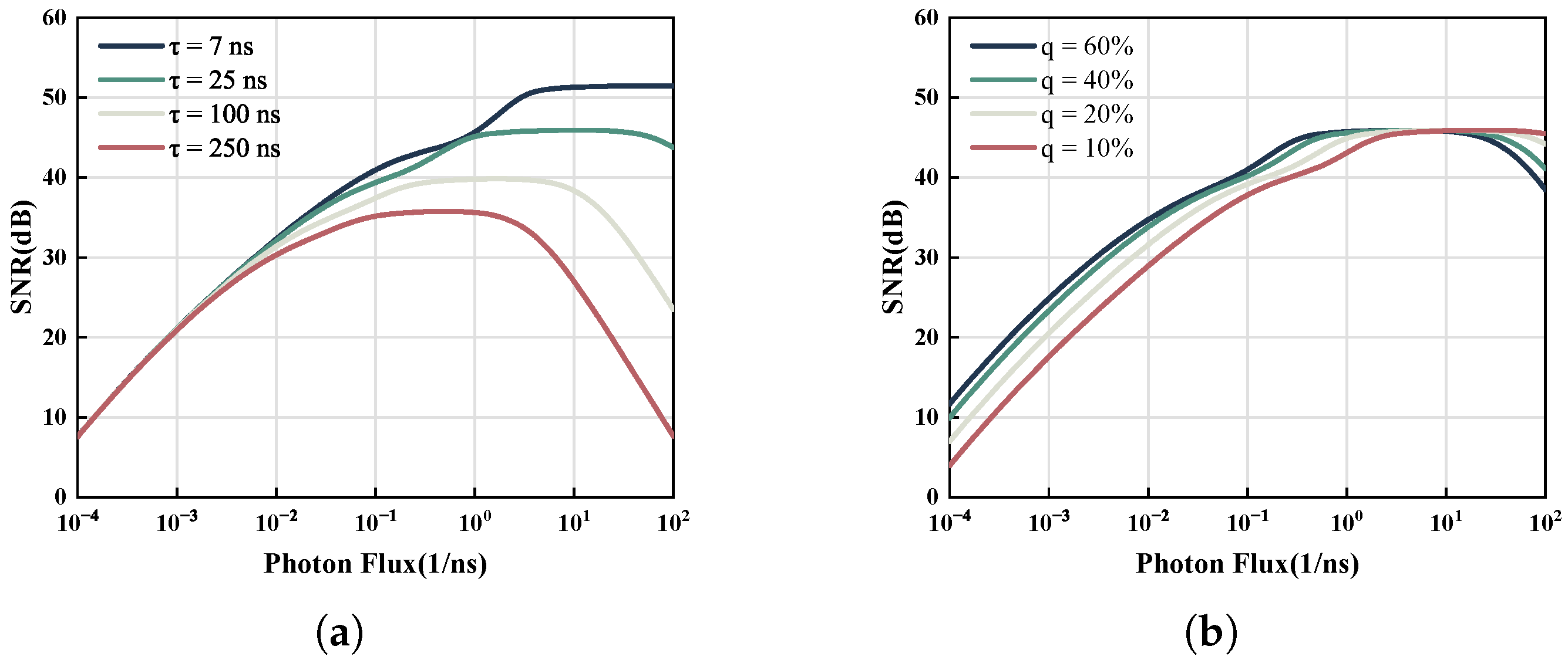
Factors such as exposure time T, dead time τ , and photon-detection probability (PDP) p impact SNR and saturation limits. Increased exposure time can improve the SNR without affecting saturation. Therefore, we focus on the influence of τ and p. Figure 3a demonstrates the effect of τ in free-running mode. The shorter the dead time, the higher the SNR, with an elevated saturation limit suggesting that faster quenching circuits saturate more slowly. As shown in Figure 3b, enhancement in detection probability does not significantly improve the SNR. Moreover, there is minimal potential for improvement in p within the visible light band.
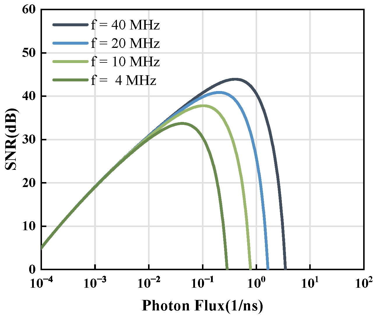
For the gating mode, we examine the effect of dead time τ on the SNR. The result is depicted in Figure 4, where q is 23% over a period of 1 ms. The frequency of the pulse signal applied to the switching MOS tube determines the dead time: 40 MHz equates to 25 ns, 20 MHz to 50 ns, 10 MHz to 100 ns, and 4 MHz to 250 ns. At lower-light intensities, the differences among these four curves are minimal. As the light intensity increases, high-frequency quenching methods yield greater SNR and a higher saturation limit.
The dead time and photon-detection probability influence the trends of the SNR and saturation limit for both imaging modes similarly. The influence of p is less significant and can be disregarded when the difference is small.

3. Experiment System

Despite theoretical exploration, practical factors remain unaccounted for, necessitating an experimental approach to validate the theory. We designed and fabricated two chips for our experiments using 180 nm CMOS technology. One chip is equipped with free-running quenching circuits with 512 × 256 pixels, while the other uses gating quenching circuits with 256 × 2 pixels. To diminish the impact of differences between pixels, we used a rolling imaging strategy. Both chips function equivalently to a rolling image chip with 256 × 1 pixels. This section introduces the two chips in terms of pixels, quenching circuits, and imaging systems.

3.1. SPAD Image Sensor Chip

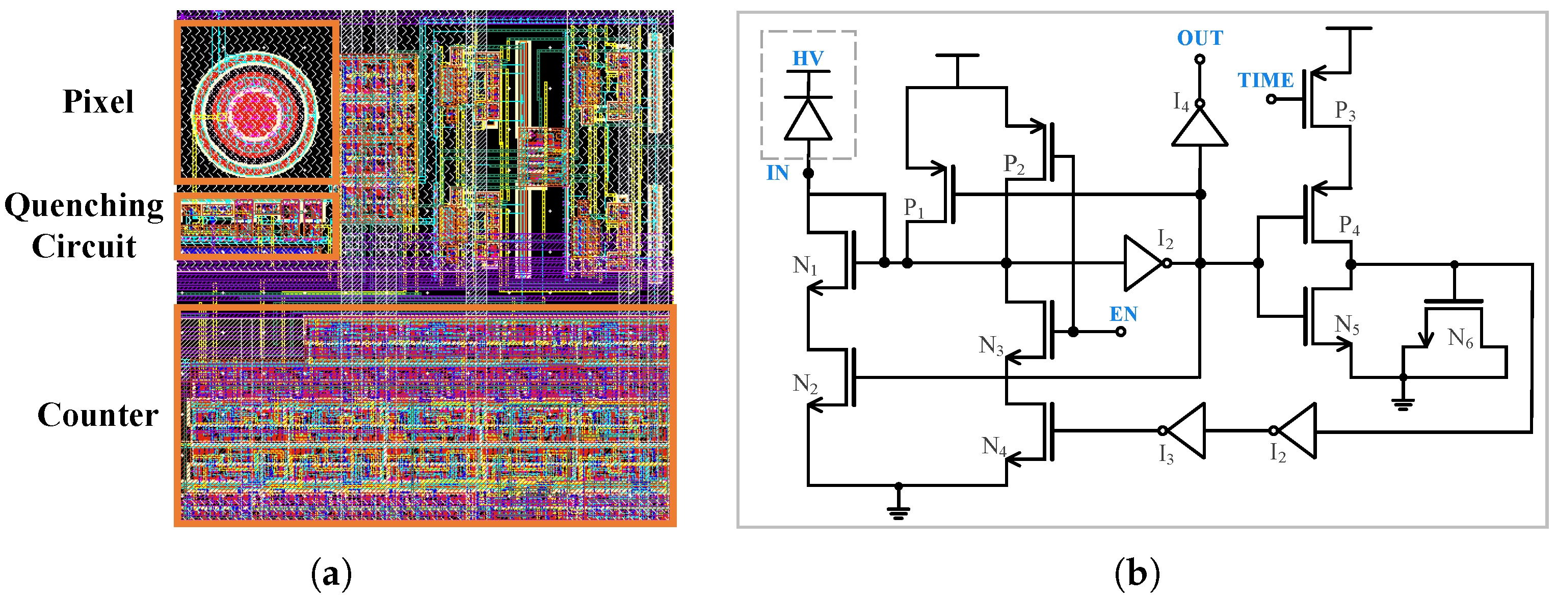
As illustrated in Figure 5a, the free-running chip with 512 × 256 pixels consists of pixels, quenching circuits, photon counters, and readout circuits, which are on the periphery of the overall circuit. The other part of the circuit that is not illustrated in Figure 5a is used for other functions not related to this article. The cathode of each pixel is connected directly to the quenching circuit, converting the light information into a digital signal. The synchronous photon counter calculates the digital pulses and locks after an exposure period. Finally, data are sent to the FIFO of the FPGA through a rolling readout system. As for the rolling imaging strategy, only one column of pixels works and is read out at a time.
The free-running chip has pixels with a diameter of 6 μ m. The pixels utilize a shallow junction with deep depletion to increase the probability of photon detection. The breakdown voltage is measured on a Cascade 12 semi-automated probe station as 11.2 V.
The free-running chip employs active quenching circuits, as shown in Figure 5b. This circuit connects the SPAD sensor to a photon counter, achieving a dead time of 7 ns. Signal EN activates the quenching process, while TIME controls the output pulse width. To accommodate rapid quenching, P 1 facilitates voltage increase when the avalanche current arrives, and the circuit branch with N 4 aids device recovery after the voltage rise. Processed digital pulses are outputted from the OUT port.
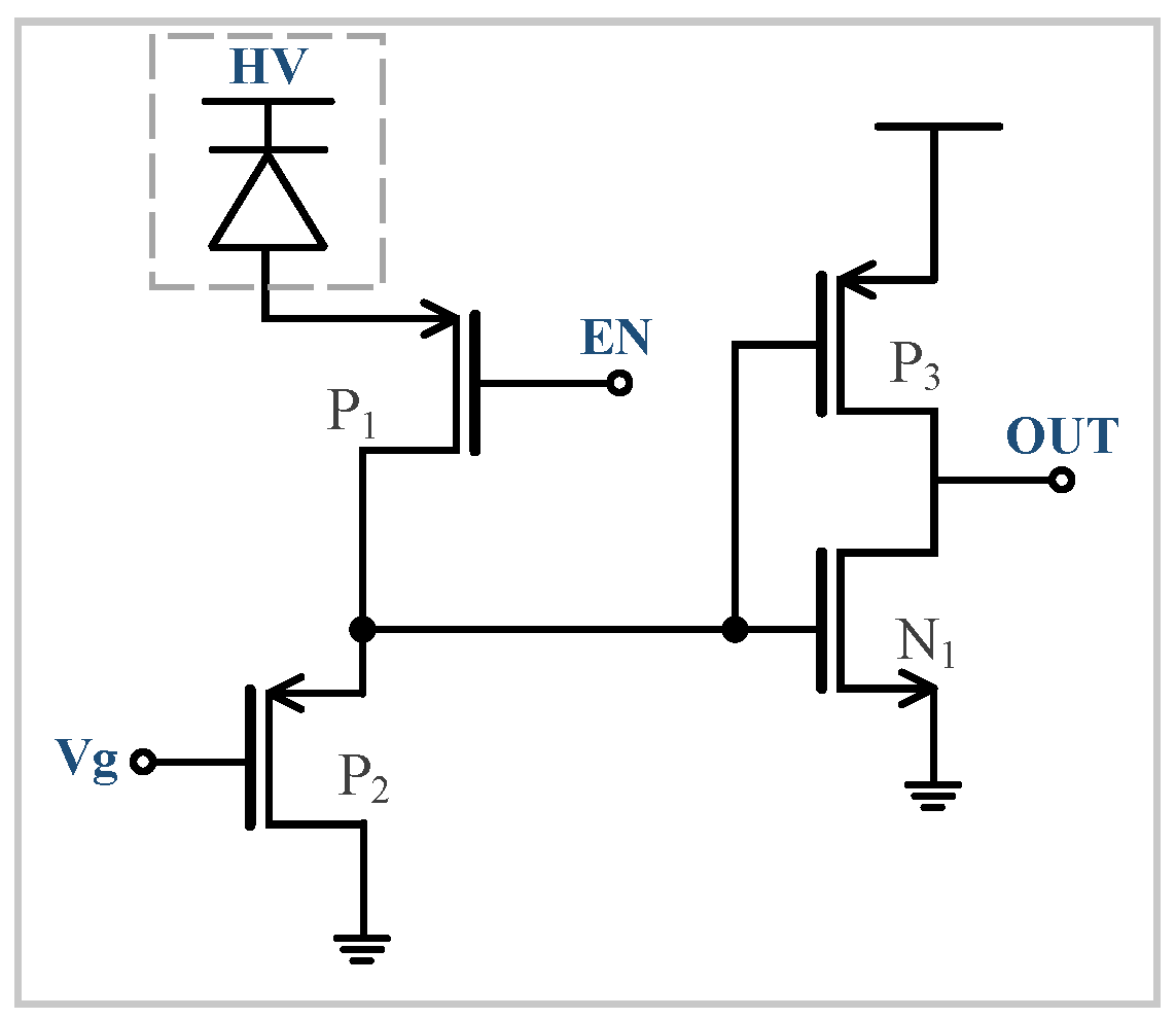
The gating chip has circuits and pixels with the same structure as the free-running chips. The gating chip uses a passive quenching circuit controlled by a gated MOS tube, as shown in Figure 6. When the gate of P 2 is opened by Vg, the bias voltage HV is applied to the SPAD. When P 2 closes, the charge is released to the ground. The gating quenching circuit tolerates a gating frequency of up to 40 MHz, resulting in a detection cycle of 25 ns. For convenience, the duty cycle of the Vg pulse operates at 50%, providing an effective detection window τ of 12.5 ns.
Comparing these quenching circuits, the free-running circuit uses 18 MOS tubes, while the gating circuit has only four transistors. While the free-running quenching circuit achieves a shorter dead time, which is beneficial for 3D imaging, it also consumes more layout area, leading to power consumption and fill-factor issues. The gating circuit, although not reaching the same high quenching frequency, meets the needs of chips with stringent area constraints.
Although the two types of chips have the same structure, the pixels have different doping conditions. Therefore, we introduce an experiment to measure the PDP to ensure the pixels of two chips have the same photon-detection ability.

3.2. Pixel Photon-Detection Probability

For consistency, we utilize pixels with similar effective areas and PDP. We characterize the PDP at various wavelengths to ensure minimal differences between the two chips. Photon counts are detected under a uniform laser generated through an integrating sphere, with the number and wavelength of incident photons precisely controlled by a laser source. Since photon counts are linearly proportional to the number of incident photons detected using an optical power meter, PDP [41] is defined as the slope of photon counts N T per area to the number of incident photons per area:
p λ = N T ν S p r o b e T P λ S s p a d ,
where ν represents the frequency of light, T is the exposure time, and P λ is the optical power at a specific light wavelength λ . S p r o b e and S s p a d are the photon-sensitive areas of the detector probe and pixel, respectively. The probe diameter is 1 cm.
Within the wavelength range of 400 nm to 760 nm, PDP peaks around the 450 nm wavelength, as shown in Figure 7. Given that most imaging applications operate within the visible light spectrum, we focus on this range. Free-running chip pixels offer a higher detection probability than gating chips, but the difference is less than 5%, which can be disregarded. Additionally, as demonstrated in Figure 3, PDP has a negligible impact on the SNR, allowing us to simplify calculations by ignoring differences in detection probability p.

3.3. Imaging System

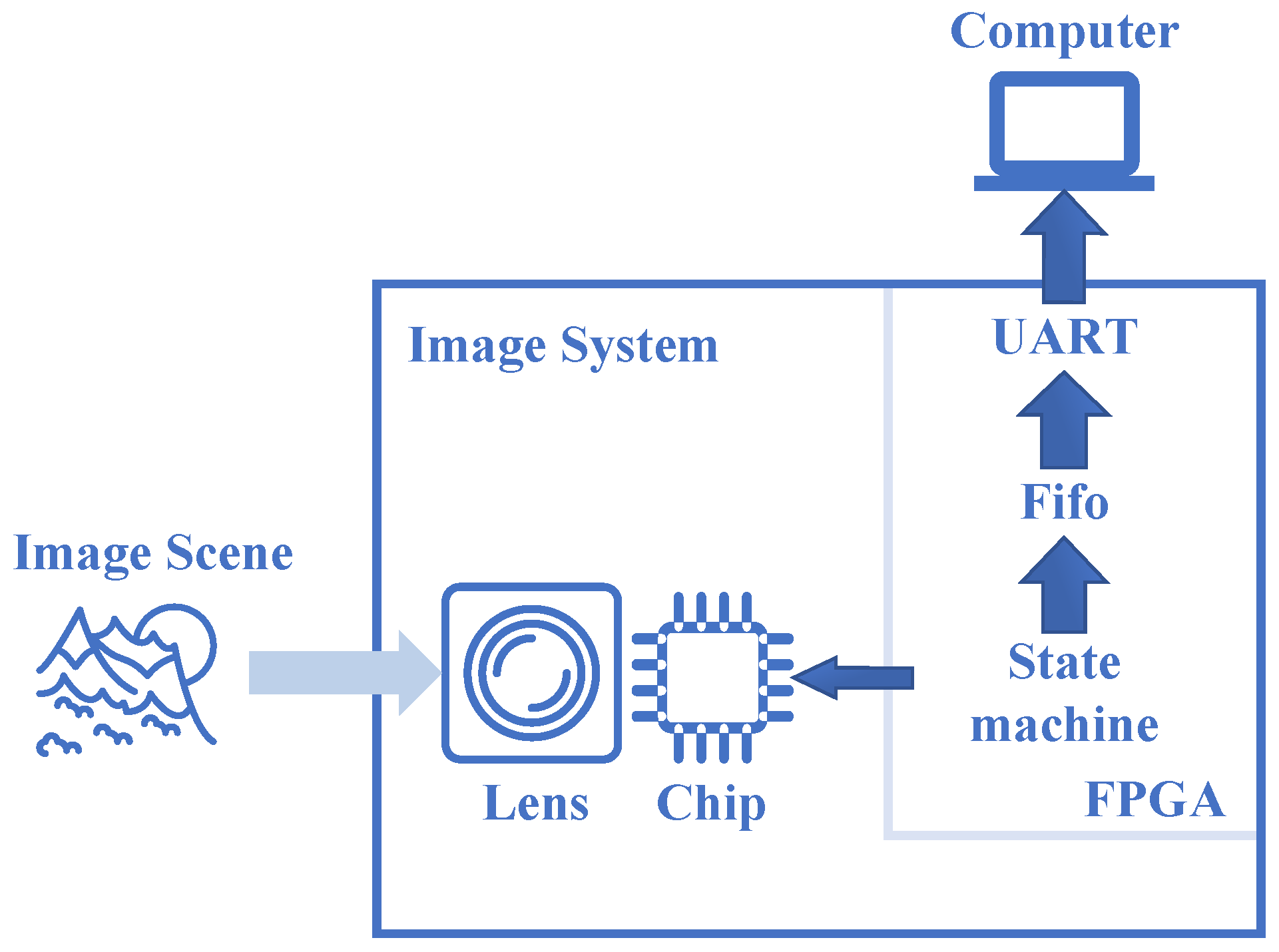
The imaging system comprises a lens, a SPAD imaging chip, and an FPGA system, as shown in Figure 8. The chip and FPGA are connected through a PCB, which also supplies power. Data from the chip are transmitted to the FPGA, which sends control signals to the chip.
We use the Cyclone IV FPGA series designed by Altera, specifically the EP4CE15F17C8 model, which is responsible for timing control and data transfer. The FPGA’s internal control system includes several modules, such as the PLL module, state machine, asynchronous FIFO, and UART data readout module.
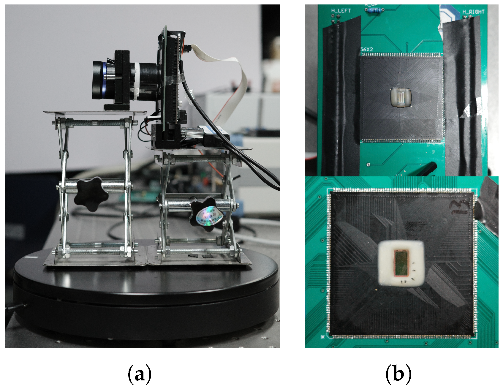
Figure 9a showcases the experimental imaging system, while Figure 9b presents pictures of the gating chip (upper image) and free-running chip (lower image). The chip is placed on a turntable with a 35 mm camera lens for line scan imaging. Due to the scanning method, slight discrepancies may appear in the captured images.

4. Experiment Results and Discussions

In this section, we present the photon count, SNR curves, and images captured by the two chips during experiments. This validation process substantiates the proposed theoretical models. Finally, we will analyze potential non-ideal noise elements.

4.1. Validation of Theoretical Models by Curves

To model the real imaging process, various parameters need to be quantified. The dead time of the free-running chip and gating chip is calculated by detecting the saturation photon count. The outcome for the free-running chip is 7 ns, and that of the gating chip is 12.5 ns under a 40 MHz gating frequency. The effective exposure time is 1 ms, and the PDP is 20%, quantified by the results in Figure 7.
To avoid deviations from pixel-to-pixel variability, data collection is confined to a single pixel. We estimate the light intensity ϕ ^ p h o t o n from the photon count N T according to a mapping relationship, and the dark noise intensity ϕ ^ d a r k is determined by dark counts. The SNR is calculated using Formula (15).
S N R = 20 log ϕ ^ p h o t o n R M S E ( ϕ ^ p h o t o n ) + R M S E ( ϕ ^ d a r k ) ,
where ϕ ^ p h o t o n = ϕ ^ ( N p h o t o n N d a r k ) and ϕ ^ d a r k = ϕ ^ ( N d a r k ) .
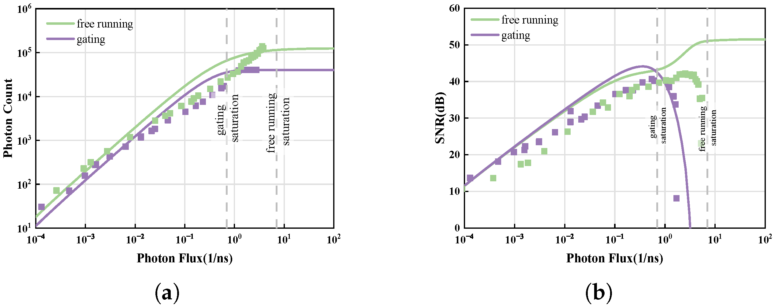
For comparison, both the theoretical and experimental curves are shown in Figure 10. The lines depict theoretical curves, while the dots present experimental results. Saturation limits are explicitly marked in the theoretical images. The higher green curves represent the free-running mode, and the purple curves represent the gating mode.
Figure 10a displays photon count curves, with the free-running mode recording more photons than the gating mode, consistent with the theory. The gating mode saturates at a much lower limit than the free-running mode, indicating that it is more prone to saturation. Before saturation, the photon count in the experiment was slightly lower than in theory, which may have been caused by experimental error in the light-intensity measurement. The photon count in the free-running mode under extremely high light intensity cannot be measured, potentially due to the active quenching circuit. These non-ideal factors are discussed in the following section.
In Figure 10b, the SNR increases with the rising light intensity before rapidly declining upon reaching saturation, aligning with theoretical predictions. The free-running mode sustains a saturation limit approximately ten times that of the gating mode, making it more suitable for imaging scenarios with significant light-intensity variations, such as outdoor environments. In low-light intensity environments, the SNR in the gating mode exceeds that of the free-running mode, making the gating mode better suited for indoor environments. The overall SNR in the experiment is lower in theory, as also seen in Figure 10a. This discrepancy is likely due to experimental error. The non-ideal properties, such as the earlier saturation of the free-running mode, will be discussed at the end of this section.
We also conducted experiments to validate the influence of pulse frequency on the SNR in the gating mode. Figure 11 shows the SNR across four different frequencies, indicating little difference under low light. At higher light intensity, the saturation limits increase with frequency, aligning well with the theoretical curves in Figure 4.

4.2. Imaging Comparison in Bright Scenes

Figure 12 illustrates the impact of the mapping method. Figure 12a shows the original image obtained from the SPAD sensor operating in the free-running mode, while Figure 12b presents the result after applying the mapping method. Details of the building exterior, characterized by higher light intensity, can be distinguished after mapping, while the interior scene remains unchanged. This behavior arises from the linear mapping relationship in low-light conditions and the nonlinear relationship in high-light intensity.
To illustrate the disparities in the SNR between the two imaging modes intuitively, we present images captured by both chips. Both images portray the same scene: a building viewed through a window on a sunny day. To mitigate errors caused by differences in pixels, image processing involves a flat-field correction method [42]. To calculate the sensor offset and calibrate the pixel response, we obtained a dark image and a light image. The calculation method is expressed as follows:
ϕ f f = k · ϕ ^ p h o t o n ϕ ^ d a r k ϕ ^ l i g h t ϕ ^ d a r k .
k is the brightness factor, referred to as the image brightness. ϕ ^ p h o t o n , ϕ ^ d a r k , and ϕ ^ l i g h t are based on the photon count without light and under an uniform-plane light source, respectively.
Images taken in bright environments are depicted in Figure 13, captured by the free-running chip and the gating chip. We equalized the brightness of the buildings in two images by adjusting the factor k. The left image indicates that the free-running chip can distinguish wall textures. In the right image taken in the gating mode, the brightest areas, those exposed to direct sunlight, appear saturated. Moreover, the highlighted part of the tree branch seems overexposed with the loss of texture details in the gating image. These observations suggest that the free-running chip has a superior saturation limit, allowing it to operate effectively across a broader range of brightness compared to the gating chip. Consequently, the free-running mode presents a notable advantage in outdoor environments.
Figure 14 presents a comparison of different frequencies in the gating mode. These images were captured at 40 MHz, 20 MHz, 10 MHz, and 4 MHz, respectively, on a cloudy day without direct sunlight. Figure 14a exhibits superior image quality and less noise than others. The brightest part of the last image, that of the building exterior, is saturated. This saturation effect even influences the entire column, reinforcing the conclusion that extended dead times will reduce saturation limits.

4.3. Imaging Comparison in Darker Scenes

We set up a darker imaging scene in a dark room, enabling us to adjust the light intensity. In this scenario, we evaluated the SNR within a specified area of the images by incorporating a blank sheet of A4 paper into the scene. The images in Figure 15 were processed through the flat-field correction method and log transformation. Logarithmic transformation [43] can amplify details in the lower gray-scale portion of the image while compressing the high-gray-scale areas. This transformation can be mathematically represented as follows:
ϕ ^ l o g = k · log v + 1 ( 1 + v · r ) .
k controls the brightness, r ϵ [0,1] signifies the normalized light intensity, and v adjusts the degree of logarithmic compression. This method significantly enhances image quality in low-light conditions; we set v to 20 in the experiments.
The clock image captured by the gating chip, in the part circled in red, displays better image uniformity than the one taken in the free-running mode, suggesting that the gating mode has an advantage in darker scenarios. In indoor environments, the gating mode is preferred.
Figure 16 presents images captured by the four-frequency gating chip under an optical power of 8 uw. The images are processed via the flat-field correction method with the same factor k. As the gating frequency increases, there is a corresponding increase in photon count, enhancing the image’s brightness and resolution. For instance, Figure 16d, captured using a gating chip at a frequency of 4 MHz, displays the lowest brightness. Correspondingly, the calculated SNR with a lower gating frequency is lower.
To quantify the difference in image quality, we calculated the SNR of the blank paper in different imaging scenes. The computed image data underwent flat-field correction to eliminate noises caused by uneven pixels. Table 1 displays the results in four different indoor light intensities. The first row’s optical power was detected by an optical power meter placed in front of the camera lens. The results indicate that the SNR of the free-running chip is lower than in the gating mode by approximately 3 dB to 5 dB. The four gating chips with different frequencies exhibit minimal variation in low-light scenes.

4.4. Discussion

In this section, we will discuss the non-ideal factors that impact SPAD image quality.
During the experiments, we observed that charge release is limited, causing the voltage to rise above the detection threshold even in the absence of photons. The SPAD quenching process involves an avalanche and charge release to reset the sensor. When light intensity becomes extremely high, it becomes difficult to fully release the charge, resulting in increased after-pulsing noise [44]. Extremely high light intensity increases the voltage, making photon detection unstable, resulting in the phenomenon where the light count in the free-running mode becomes immeasurable.
Recharge errors significantly impact the entry and exit processes of SPADs into and out of their dead time, causing deviations from the expected exponential distribution in inter-photon time intervals. As previously discussed, dead time is theoretically determined based on the saturation photon count. Specifically, after saturation, the time between pulses shortens as the next photon is detected, and an avalanche begins before the previous one is fully quenched. This results in a shorter effective dead time in the free-running mode compared to its pre-saturation duration. In contrast, the gating mode imposes a fixed pulse frequency, thereby fixing the dead time. Consequently, under low-light conditions, the signal-to-noise Ratio (SNR) theoretically favors the free-running mode over the gating mode, contrary to experimental observations noted in prior studies [25].
Additionally, we observed that the free-running mode tends to saturate earlier, likely due to high-frequency quenching. As incident photons become more concentrated, the number of active SPAD pixels increases, resulting in higher power consumption. Specifically, with a 7 ns dead time in the free-running mode, the heating effect becomes more pronounced. As the temperature rises, the impact of dark noise increases, approximately doubling the dark count rate for every 20 K increase in temperature [45]. This also affects active quenching, preventing the free-running mode from functioning properly beyond a certain light intensity. Due to the use of the mapping method, at high-light intensity ranges, small differences in photon counting result in significant differences in mapped light flux. When dark noise becomes significant in photon counts, the mapping method amplifies this noise.

5. Conclusions

SPAD sensors show great promise as image sensors due to their sensitivity at the single-photon level and in high-dynamic ranges. In SPAD imaging, photon detection is crucial. The quenching mode not only affects the photon-detection capability and power consumption but also influences the imaging SNR and dynamic range. In this study, we proposed a theoretical model for SPAD imaging, focusing on the impact of two imaging modes, the free-running and gating modes, on imaging performance.
Firstly, we derived theoretical models for the free-running and gating imaging modes based on the Poisson distribution theory of incident photons. These models reveal the nonlinear response characteristics and high-dynamic range features of SPAD imaging. Additionally, we derived and validated theoretical formulas for noise and the SNR.
Secondly, we designed and fabricated two SPAD imaging chips using 180 nm CMOS technology, equipped with free-running and gating imaging modes. A rotating imaging system was built to achieve imaging with a 256 × 1 equivalent line array scale.
Thirdly, we conducted a comprehensive evaluation and analysis of image quality. Using mapping methods, we compared the two imaging modes under various light-intensity conditions. Experimental results validated the theoretical model and revealed that the free-running mode exhibits a higher saturation limit and is suitable for outdoor environments with high light intensity. In contrast, the gating mode demonstrates superior linearity and low noise characteristics, making it ideal for indoor imaging.
This study provides a solid foundation for a deeper understanding of the working principles and characteristics of SPAD image sensors. Furthermore, it offers theoretical guidance for optimizing and improving SPAD imaging in various academic and practical applications.

Author Contributions

Methodology, X.K.; software, H.Y.; validation, H.H. and X.S.; formal analysis, X.S.; investigation, X.S.; writing—original draft preparation, X.S.; writing—review and editing, C.M. and X.K; supervision, F.Y. All authors have read and agreed to the published version of the manuscript.

Funding

This research received no external funding.

Institutional Review Board Statement

Not applicable.

Informed Consent Statement

Not applicable.

Data Availability Statement

Data are contained within the article.

Conflicts of Interest

The authors declare no conflicts of interest.

References

  1. Schaart, D.R.; Schramm, G.; Nuyts, J.; Surti, S. Time of flight in perspective: Instrumental and computational aspects of time resolution in positron emission tomography. IEEE Trans. Radiat. Plasma Med. Sci. 2021, 5, 598–618. [Google Scholar] [CrossRef]
  2. Keshavarzian, P.; Ramu, K.; Tang, D.; Weill, C.; Gramuglia, F.; Tan, S.S.; Tng, M.; Lim, L.; Quek, E.; Mandich, D.; et al. A 3.3-Gb/s SPAD-based quantum random number generator. IEEE J. Solid-State Circuits 2023, 58, 2632–2647. [Google Scholar] [CrossRef]
  3. Leone, N.; Rusca, D.; Azzini, S.; Fontana, G.; Acerbi, F.; Gola, A.; Tontini, A.; Massari, N.; Zbinden, H.; Pavesi, L. An optical chip for self-testing quantum random number generation. APL Photonics 2020, 5, 101301. [Google Scholar] [CrossRef]
  4. Kumagai, O.; Ohmachi, J.; Matsumura, M.; Yagi, S.; Tayu, K.; Amagawa, K.; Matsukawa, T.; Ozawa, O.; Hirono, D.; Shinozuka, Y.; et al. 7.3 A 189 × 600 Back-Illuminated Stacked SPAD Direct Time-of-Flight Depth Sensor for Automotive LiDAR Systems. In Proceedings of the 2021 IEEE International Solid- State Circuits Conference (ISSCC), San Francisco, CA, USA, 13–22 February 2021; Volume 64, pp. 110–112. [Google Scholar] [CrossRef]
  5. Villa, F.; Severini, F.; Madonini, F.; Zappa, F. SPADs and SiPMs arrays for long-range high-speed light detection and ranging (LiDAR). Sensors 2021, 21, 3839. [Google Scholar] [CrossRef] [PubMed]
  6. Smith, J.T.; Rudkouskaya, A.; Gao, S.; Gupta, J.M.; Ulku, A.; Bruschini, C.; Charbon, E.; Weiss, S.; Barroso, M.; Intes, X.; et al. In vitro and in vivo NIR fluorescence lifetime imaging with a time-gated SPAD camera. Optica 2022, 9, 532–544. [Google Scholar] [CrossRef] [PubMed]
  7. Zickus, V.; Wu, M.L.; Morimoto, K.; Kapitany, V.; Fatima, A.; Turpin, A.; Insall, R.; Whitelaw, J.; Machesky, L.; Bruschini, C.; et al. Wide-field Fluorescence Lifetime Imaging Microscopy with a High-Speed Mega-pixel SPAD Camera. bioRxiv 2020. Available online: https://www.biorxiv.org/content/early/2020/06/08/2020.06.07.138685.full.pdf (accessed on 8 June 2020). [CrossRef]
  8. Ghezzi, A.; Farina, A.; Bassi, A.; Valentini, G.; Labanca, I.; Acconcia, G.; Rech, I.; D’Andrea, C. Multispectral compressive fluorescence lifetime imaging microscopy with a SPAD array detector. Opt. Lett. 2021, 46, 1353–1356. [Google Scholar] [CrossRef]
  9. Ma, J.; Chan, S.; Fossum, E.R. Review of Quanta Image Sensors for Ultralow-Light Imaging. IEEE Trans. Electron. Devices 2022, 69, 2824–2839. [Google Scholar] [CrossRef]
  10. Afshar, S.; Hamilton, T.J.; Davis, L.; Van Schaik, A.; Delic, D. Event-Based Processing of Single Photon Avalanche Diode Sensors. IEEE Sens. J. 2020, 20, 7677–7691. [Google Scholar] [CrossRef]
  11. Kong, X.; Mao, C.; Hu, X.; Yan, F. Time-Delay-Integration Imaging Implemented with Single-Photon-Avalanche-Diode Linear Array. IEEE Sens. J. 2021, 21, 6012–6023. [Google Scholar] [CrossRef]
  12. Morimoto, K.; Ardelean, A.; Wu, M.L.; Ulku, A.C.; Antolovic, I.M.; Bruschini, C.; Charbon, E. Megapixel time-gated SPAD image sensor for 2D and 3D imaging applications. Optica 2020, 7, 346–354. [Google Scholar] [CrossRef]
  13. Ogi, J.; Takatsuka, T.; Hizu, K.; Inaoka, Y.; Zhu, H.; Tochigi, Y.; Tashiro, Y.; Sano, F.; Murakawa, Y.; Nakamura, M.; et al. 7.5 A 250fps 124dB Dynamic-Range SPAD Image Sensor Stacked with Pixel-Parallel Photon Counter Employing Sub-Frame Extrapolating Architecture for Motion Artifact Suppression. In Proceedings of the 2021 IEEE International Solid- State Circuits Conference (ISSCC), San Francisco, CA, USA, 13–22 February 2021; Volume 64, pp. 113–115. [Google Scholar] [CrossRef]
  14. Erdogan, A.T.; Al Abbas, T.; Finlayson, N.; Hopkinson, C.; Gyongy, I.; Almer, O.; Dutton, N.A.; Henderson, R.K. A high dynamic range 128× 120 3-D stacked CMOS SPAD image sensor SoC for fluorescence microendoscopy. IEEE J. Solid-State Circuits 2022, 57, 1649–1660. [Google Scholar] [CrossRef]
  15. Liu, Y.; Gutierrez-Barragan, F.; Ingle, A.; Gupta, M.; Velten, A. Single-photon camera guided extreme dynamic range imaging. In Proceedings of the IEEE/CVF Winter Conference on Applications of Computer Vision, Waikoloa, HI, USA, 3–8 January 2022; pp. 1575–1585. [Google Scholar]
  16. Wang, Z.; Zhang, J.; Lin, M.; Wang, J.; Luo, P.; Ren, J. Learning a reinforced agent for flexible exposure bracketing selection. In Proceedings of the IEEE/CVF conference on computer vision and pattern recognition, Seattle, WA, USA, 14–19 June 2020; pp. 1820–1828. [Google Scholar]
  17. Niu, Y.; Wu, J.; Liu, W.; Guo, W.; Lau, R.W. Hdr-gan: Hdr image reconstruction from multi-exposed ldr images with large motions. IEEE Trans. Image Process. 2021, 30, 3885–3896. [Google Scholar] [CrossRef] [PubMed]
  18. Wang, L.; Yoon, K.J. Deep learning for hdr imaging: State-of-the-art and future trends. IEEE Trans. Pattern Anal. Mach. Intell. 2021, 44, 8874–8895. [Google Scholar] [CrossRef]
  19. Chi, Y.; Zhang, X.; Chan, S.H. Hdr imaging with spatially varying signal-to-noise ratios. In Proceedings of the IEEE/CVF Conference on Computer Vision and Pattern Recognition, Vancouver, BC, Canada, 17–24 June 2023; pp. 5724–5734. [Google Scholar]
  20. Jiang, W.; Scott, R.; Deen, M.J. Differential quench and reset circuit for single-photon avalanche diodes. J. Light. Technol. 2021, 39, 7334–7342. [Google Scholar] [CrossRef]
  21. Dervić, A.; Hofbauer, M.; Goll, B.; Zimmermann, H. High slew-rate quadruple-voltage mixed-quenching active-resetting circuit for SPADs in 0.35-μm CMOS for increasing PDP. IEEE Solid-State Circuits Lett. 2020, 4, 18–21. [Google Scholar] [CrossRef]
  22. Jiang, W.; Chalich, Y.; Scott, R.; Deen, M.J. Time-gated and multi-junction SPADs in standard 65 nm CMOS technology. IEEE Sens. J. 2021, 21, 12092–12103. [Google Scholar] [CrossRef]
  23. Xu, Y.; Lu, J.; Wu, Z. A compact high-speed active quenching and recharging circuit for SPAD detectors. IEEE Photonics J. 2020, 12, 1–8. [Google Scholar] [CrossRef]
  24. Jiang, W.; Scott, R.; Deen, M.J. High-Speed Active Quench and Reset Circuit for SPAD in a Standard 65 nm CMOS Technology. IEEE Photonics Technol. Lett. 2021, 33, 1431–1434. [Google Scholar] [CrossRef]
  25. Ingle, A.; Seets, T.; Buttafava, M.; Gupta, S.; Tosi, A.; Gupta, M.; Velten, A. Passive inter-photon imaging. In Proceedings of the IEEE/CVF Conference on Computer Vision and Pattern Recognition, Nashville, TN, USA, 20–25 June 2021; pp. 8585–8595. [Google Scholar]
  26. Park, S.Y.; Kim, H.J. CMOS image sensor with two-step single-slope ADC using differential ramp generator. IEEE Trans. Electron Devices 2021, 68, 4966–4971. [Google Scholar] [CrossRef]
  27. Glauber, R.J. Photon correlations. Phys. Rev. Lett. 1963, 10, 84. [Google Scholar] [CrossRef]
  28. Rempe, G.; Schmidt-Kaler, F.; Walther, H. Observation of sub-Poissonian photon statistics in a micromaser. Phys. Rev. Lett. 1990, 64, 2783. [Google Scholar] [CrossRef] [PubMed]
  29. Scholes, S.; Mora-Martín, G.; Zhu, F.; Gyongy, I.; Soan, P.; Leach, J. Fundamental limits to depth imaging with single-photon detector array sensors. Sci. Rep. 2023, 13, 176. [Google Scholar] [CrossRef] [PubMed]
  30. Ingle, A.; Velten, A.; Gupta, M. High flux passive imaging with single-photon sensors. In Proceedings of the IEEE/CVF Conference on Computer Vision and Pattern Recognition, Long Beach, CA, USA, 15–20 June 2019; pp. 6760–6769. [Google Scholar]
  31. Tangudu, J.; Gunturi, S.; Jalan, S.; Janardhanan, J.; Ganesan, R.; Sahu, D.; Waheed, K.; Wallberg, J.; Staszewski, R.B. Quantization noise improvement of time to digital converter (TDC) for ADPLL. In Proceedings of the 2009 IEEE International Symposium on Circuits and Systems, Taipei, Taiwan, 24–27 May 2009; pp. 1020–1023. [Google Scholar]
  32. Ota, Y.; Morimoto, K.; Sasago, T.; Shinohara, M.; Kuroda, Y.; Endo, W.; Maehashi, Y.; Maekawa, S.; Tsuchiya, H.; Abdelahafar, A.; et al. A 0.37 W 143dB-dynamic-range 1Mpixel backside-illuminated charge-focusing SPAD image sensor with pixel-wise exposure control and adaptive clocked recharging. In Proceedings of the 2022 IEEE International Solid-State Circuits Conference (ISSCC), San Francisco, CA, USA, 20–26 February 2022; Volume 65, pp. 94–96. [Google Scholar]
  33. Cushen, C.D.; Hudson, R.L. A quantum-mechanical central limit theorem. J. Appl. Probab. 1971, 8, 454–469. [Google Scholar] [CrossRef]
  34. Beenakker, C.; Schönenberger, C. Quantum shot noise. Phys. Today 2003, 56, 37–42. [Google Scholar] [CrossRef]
  35. Dutton, N.A.; Gyongy, I.; Parmesan, L.; Gnecchi, S.; Calder, N.; Rae, B.R.; Pellegrini, S.; Grant, L.A.; Henderson, R.K. A SPAD-based QVGA image sensor for single-photon counting and quanta imaging. IEEE Trans. Electron Devices 2015, 63, 189–196. [Google Scholar] [CrossRef]
  36. Yuan, Z.; Kardynal, B.; Sharpe, A.; Shields, A. High speed single photon detection in the near infrared. Appl. Phys. Lett. 2007, 91, 041114. [Google Scholar] [CrossRef]
  37. Fishburn, M.W.; Charbon, E. System Tradeoffs in Gamma-Ray Detection Utilizing SPAD Arrays and Scintillators. IEEE Trans. Nucl. Sci. 2010, 57, 2549–2557. [Google Scholar] [CrossRef]
  38. Mu, Y.; Wang, C.; Xu, Y.B.; Du, X.X.; Pan, Q.Y.; Zhang, H.Y.; Zhu, Y.J. Time-coordinated SPAD-based receiver for high-speed optical wireless communication. Opt. Commun. 2023, 526, 128706. [Google Scholar] [CrossRef]
  39. Altham, P.M. Two generalizations of the binomial distribution. J. R. Stat. Soc. Ser. C Appl. Stat. 1978, 27, 162–167. [Google Scholar] [CrossRef]
  40. Edwards, A. The meaning of binomial distribution. Nature 1960, 186, 1074. [Google Scholar] [CrossRef] [PubMed]
  41. Gramuglia, F.; Wu, M.L.; Bruschini, C.; Lee, M.J.; Charbon, E. A low-noise CMOS SPAD pixel with 12.1 ps SPTR and 3 ns dead time. IEEE J. Sel. Top. Quantum Electron. 2021, 28, 1–9. [Google Scholar] [CrossRef]
  42. Seibert, J.A.; Boone, J.M.; Lindfors, K.K. Flat-field correction technique for digital detectors. In Proceedings of the Medical Imaging 1998: Physics of Medical Imaging, San Diego, CA, USA, 21–26 February 1998; Volume 3336, pp. 348–354. [Google Scholar]
  43. Wang, W.; Wu, X.; Yuan, X.; Gao, Z. An experiment-based review of low-light image enhancement methods. IEEE Access 2020, 8, 87884–87917. [Google Scholar] [CrossRef]
  44. Cheng, Z.; Zheng, X.; Palubiak, D.; Deen, M.J.; Peng, H. A Comprehensive and Accurate Analytical SPAD Model for Circuit Simulation. IEEE Trans. Electron Devices 2016, 63, 1940–1948. [Google Scholar] [CrossRef]
  45. Buttafava, M.; Villa, F.; Castello, M.; Tortarolo, G.; Conca, E.; Sanzaro, M.; Piazza, S.; Bianchini, P.; Diaspro, A.; Zappa, F.; et al. SPAD-based asynchronous-readout array detectors for image-scanning microscopy. Optica 2020, 7, 755–765. [Google Scholar] [CrossRef]
Figure 1. The three different imaging modes. The first schematic diagram is a traditional camera sensor, which can detect photons constantly. The second shows the free-running mode and the third is the gating mode. Both the free-running and gating modes have nonlinear response curves.
Photonics 11 00721 g001
Figure 2. Comparison of theoretical curves for free-running and gating-quenching modes under the conditions of exposure time T = 1   ms , dead time τ = 25   ns , and photon-detection probability p = 18 % . To ensure consistency, the constants in these formulas were set to be the same. (a) The number of detected photons. (b) SNR without mapping. (c) SNR with mapping.
Photonics 11 00721 g002
Figure 3. Influence of the dead time τ and photon-detection probability p in the free-running quenching mode. The exposure time is 1 ms. (a) SNR curves for τ = 7   ns , 25   ns , 100   ns and 250   ns while p = 20 % . (b) SNR curves for p = 60 % , 40 % , 20 % , and 10 % while τ is 25 ns.
Photonics 11 00721 g003
Figure 4. The SNR curves of different frequencies predicted by Formula (6) in the gating mode, where the exposure time is 1 ms.
Photonics 11 00721 g004
Figure 5. The circuit of the free-running SPAD image chip. (a) The layout picture of a single cell in the free-running chip, including the pixel, the quenching circuit, and the counter. (b) The active quenching circuit in the free-running SPAD chips.
Photonics 11 00721 g005
Figure 6. The gating quenching circuits integrated in SPAD image chips: passive quenching circuit.
Photonics 11 00721 g006
Figure 7. Photon-detection probability of the pixels from the free-running chip and gating chip across a wavelength range of 350 nm to 950 nm. (a) Photon-detection probability of pixels in the free-running chip. (b) Photon-detection probability of pixels in the gating chip.
Photonics 11 00721 g007
Figure 8. The structure of the SPAD imaging system: the SPAD chip captures image data through a lens. These data are then processed by an FPGA, which transfers image data to a computer after caching them using an Asyn-FIFO.
Photonics 11 00721 g008
Figure 9. Experimental SPAD imaging system. (a) Imaging system containing a turntable, lens, chip, and FPGA. (b) The PCB photos of the free-running chip and gating chip.
Photonics 11 00721 g009
Figure 10. Comparison of theoretical curves and experiment results of the free-running and gating chips in the condition of exposure time T = 1   ms , photon detection probability p = 20 % , dead time τ = 7   ns , and 12.5 ns, respectively. The lines depict theoretical curves, and the dots represent experimental results. (a) Theoretical curve and experiment result of photon count. (b) Theoretical curve and experiment result of the SNR with mapping.
Photonics 11 00721 g010
Figure 11. The impact of pulse frequency on the SNR in the gating mode, with an exposure time of 1 ms.
Photonics 11 00721 g011
Figure 12. Experimental comparison of the utilization of mapping: (a) original photo captured by the free-running chip. (b) Photo after mapping processing.
Photonics 11 00721 g012
Figure 13. Pictures captured in high-brightness scenes by the free-running and gating chips in the exposure time 10 ms. The red box highlights the region affected by the saturation limit. (a) Photo captured by the free-running chip (b) Photo captured by the gating chip.
Photonics 11 00721 g013
Figure 14. Comparison of different frequencies in the gating mode with an exposure time of T = 10   ms in an outdoor environment. (a) Picture of frequency 40 MHz. (b) Picture of frequency 20 MHz. (c) Picture of frequency 10 MHz. (d) Picture of frequency 4 MHz.
Photonics 11 00721 g014
Figure 15. Pictures captured in high-brightness scenes by the free-running and gating chips with an exposure time of 10 ms. The red box highlights the region where the two pictures differ in SNR, showing the impact of the imaging mode. (a) Photo captured by the free-running chip (b) Photo captured by the gating chip.
Photonics 11 00721 g015
Figure 16. Comparison of different frequencies in the gating mode in an indoor environment. Exposure time T = 10   ms . (a) Picture of frequency 40 MHz. (b) Picture of frequency 20 MHz. (c) Picture of frequency 10 MHz. (d) Picture of frequency 4 MHz.
Photonics 11 00721 g016
Table 1. The SNR of blank paper in four different light intensities.
Optical Power5 uw8 uw10 uw12 uw
free running11.3720.7323.724.78
gating (40 MHz)15.9324.5826.4127.23
gating (20 MHz)14.7823.2824.4125.95
gating (10 MHz)14.8823.4325.2225.79
gating (4 MHz)14.5323.9825.225.6
Disclaimer/Publisher’s Note: The statements, opinions and data contained in all publications are solely those of the individual author(s) and contributor(s) and not of MDPI and/or the editor(s). MDPI and/or the editor(s) disclaim responsibility for any injury to people or property resulting from any ideas, methods, instructions or products referred to in the content.