Article

Ultra-Sensitive Refractive Index Sensing Based on Quasi-BICs in All-Dielectric Nanorod Array

1
Shandong Provincial Engineering and Technical Center of Light Manipulations & Shandong Provincial Key Laboratory of Optics and Photonic Device, School of Physics and Electronics, Shandong Normal University, Jinan 250358, China
2
Collaborative Innovation Center of Light Manipulation and Applications, Shandong Normal University, Jinan 250358, China
*
Authors to whom correspondence should be addressed.
Photonics 2024, 11(6), 503; https://doi.org/10.3390/photonics11060503
Submission received: 5 April 2024 / Revised: 21 May 2024 / Accepted: 23 May 2024 / Published: 25 May 2024
(This article belongs to the Section Lasers, Light Sources and Sensors)

Abstract

:
We propose an all-dielectric nanorod array for ultra-sensitive refractive index sensing based on quasi-bound states in the continuum (BICs). The nanorod is fabricated by silicon or silicon with an air hole, i.e., the hollow silicon nanorod. The quasi-BICs are formed in the hollow silicon nanorod array due to the symmetry-breaking of air holes. The high-quality factor (Q-factor) and ultra-narrow reflectance spectral width at quasi-BICs contribute to high performances of the sensor. The numerical results show that the sensitivity and figure of merit (FOM) can reach up to 602.9 nm/RIU and 34,977, respectively. The results indicate that the proposed nanostructures of quasi-BICs are promising for advanced biosensing applications.

1. Introduction

Optical sensing has unique and important applications in many fields, such as biomolecules [1,2], chemical detection [3], real-time biochemical reactions, or environmental monitoring [4]. Various optical technologies have been proposed for optical sensors in recent years, for example, surface plasmon resonance (SPR) [5] in metallic nanostructures. Plasma nanostructure-based sensors are susceptible to strong electric fields where the analyte is located [6]. However, plasmonic nanostructures suffer from high losses due to the intrinsic absorption of plasmonic metals [7,8,9], which results in a lower quality factor (Q-factor) and limits sensing performance. In recent years, high-refractive index dielectric nanostructures have gained attention in metasurfaces and nanoantennas [10,11] due to their efficient and flexible light control at the nanoscale and their potential for biosensing applications [10,12,13]. Optically resonant sensors are characterized not only by the shift in resonance wavelength per refractive-index-unit change (S) but also by the high Q-factor of the resonance mode, which is related with another performance of sensor, i.e., the figure of merit (FOM) [14]. And thus, the orientation to improve the performance of optical sensors is to narrow the optical spectral width and to improve the Q-factor of resonance modes in metasurfaces or nanoantennas.
In 1985, Friedrich and Wintgen proposed BICs using a generic two-level non-Hermitian Hamiltonian [15,16]. Their approach was applied to a photonic wave-guide system by Bulgakov et al. in 2008 [17] and was experimentally demonstrated by Plotnik et al. in 2011 [18].
However, BIC is symmetry-protected and cannot be observed in real systems [14]. When the structural symmetry is broken, the BIC with an infinite Q-factor can be trans-formed into quasi-BICs [19]. These quasi-BICs typically take the form of finite Q-factor and non-zero linewidth. Quasi-BICs are highly valued in nonlinear optics [20], nanolasing [21], and other areas [22,23,24,25,26] due to their high Q-factor and large electric field enhancement. Nanostructures have unique properties that make them ideal for biosensing and chemical sensing applications. Their high Q-factor and narrow linewidth make them particularly suitable for biosensing. At the same time, the attachment of chemical biomolecules to the surface of the nanostructures is critical for chemical sensing.
The quasi-BICs for sensing have been widely investigated in recent years, e.g., Li et al. proposed an all-dielectric column structure with broken symmetry that supports quasi-BICs to achieve ultrasensitive sensing in the terahertz range, and the sensitivity achieved 170.58 GHz/RIU [27]. Liu et al. proposed a dielectric corrugated structure surrounded by two monolayer graphene sheets. By introducing a phase difference between the upper and lower surfaces of dielectric grating, the symmetry of the structure was broken, and the BIC turned into quasi-BICs, with a high-sensitivity resonant mode of 810 nm/RIU and a high FOM of 5.7 × 10⁴ [28]. Samadi et al. proposed an all-dielectric silicon metasurface based on complementary split-ring resonators (CSRRs), achieving a sensitivity of 155 nm/RIU and a high FOM of 3.875×10⁵ [29]. Zhao et al. investigated an all-dielectric hypersurface with an asymmetric dielectric constant, which consists of rectangular tetramer clusters with symmetric structural parameters, by changing the material of the rectangle and the material asymmetry to achieve the asymmetry of the dielectric constant. The two sets of rectangles were made of Si and InAs, with sensitivities of 170 nm/RIU and 182 nm/RIU and FOMs of 567 and 910, respectively [30]. Wang et al. proposed an asymmetric dual-nanorod type of metasurface sensor. By adjusting the width of the nanorods, the ideal BIC was converted to quasi-BICs. The resonance frequency and linewidth could be changed by varying the asymmetry parameters of the nanorods. The sensitivity of resonant mode is 408 nm/RIU with an FOM of 107 [31]. Chen et al. proposed an asymmetric all-dielectric metasurface. The resonances could be transformed into the electric dipole and the toroidal dipole quasi-BICs’ resonance with high-quality factors by breaking the symmetry of the metasurface, with the sensitivity of resonant mode as 402 nm/RIU and an FOM of 2400 [32]. Huo et al. proposed a highly sensitive sensor based on toroidal dipole (TD) quasi-BICs. The metasurface consists of an array of single non-coaxial core-shell cylinder nanostructures with a sensitivity of 342 nm/RIU and an FOM of 1295 [14]. Cao et al. designed a multi-wavelength optical switch based on an all-dielectric metastructure consisting of four asymmetric semi-circular rings. The sensitivity and the FOM are 197 nm/RIU and 492, respectively [33]. Sun et al. designed an all-dielectric hollow nanocylinder dimer metastructure. By breaking the symmetry (height symmetry or aperture symmetry) of two hollow nanocylinders, a sensitivity of 870 nm/RIU and an FOM of 600 were achieved [34]. Chen et al. proposed a refractive index sensor with high performance by introducing an asymmetric parameter to generate quasi-BICs. The simulation results showed that the proposed metastructure had excellent sensing properties with a Q-factor of 3668, sensitivity of 350 nm/RIU, and FOM of 1000 [35].
The resonant modes of the quasi-BICs proposed so far mainly confine the electro-magnetic fields inside high-index materials. This is problematic for chemical sensors because chemical biomolecules are usually attached to the surface of nanostructures. Therefore, in order to improve the sensing performance, it is necessary to design those nanostructures that can confine electromagnetic fields in the surface region [36,37]. It has been demonstrated that nanostructures that confine electromagnetic fields in the surface region can indeed improve sensing performance. This provides us with a new idea: by designing suitable nanostructures, we can make more effective use of the properties of quasi-BICs and thus improve the performance of chemical biosensors.
In this paper, we propose an all-dielectric nanorod array for ultra-sensitive refractive index sensing based on quasi-BICs. The transformation between BIC and quasi-BICs can be controlled by varying the central through-hole offsets of the nanorod arrays. Crucially, the positions of these quasi-BICs induced by relative shifts remain nearly unchanged due to their bonding mode characteristics. The hollow silicon nanorod with an air hole is a unit of the array. The quasi-BICs are achieved by the symmetric breaking of the air hole in an individual nanorod under the ultra-high sensitivity planewave illumination and FOM are simultaneously obtained in the optimized nanostructures.

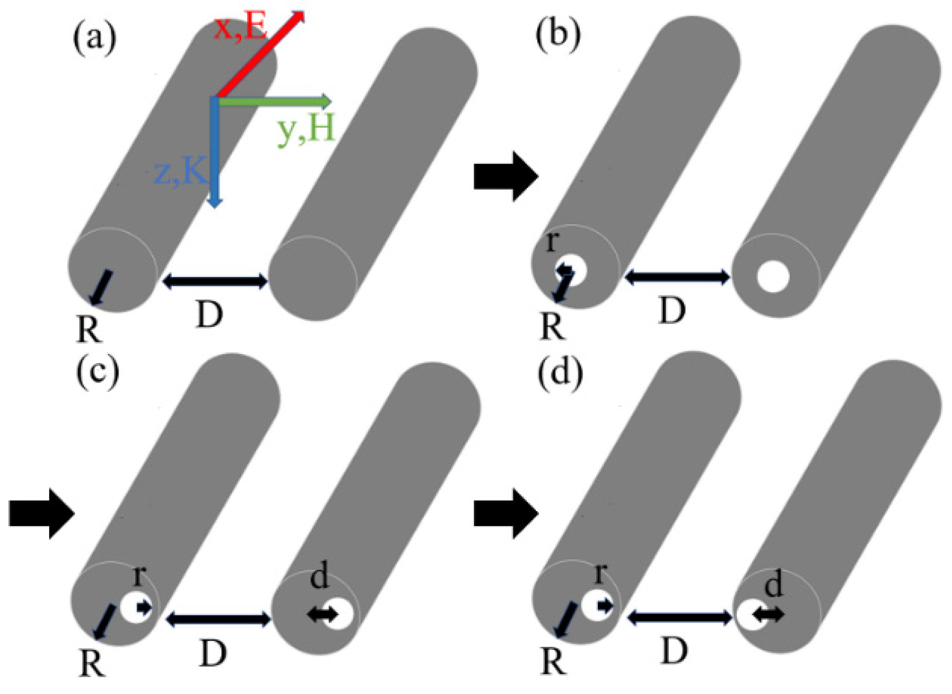
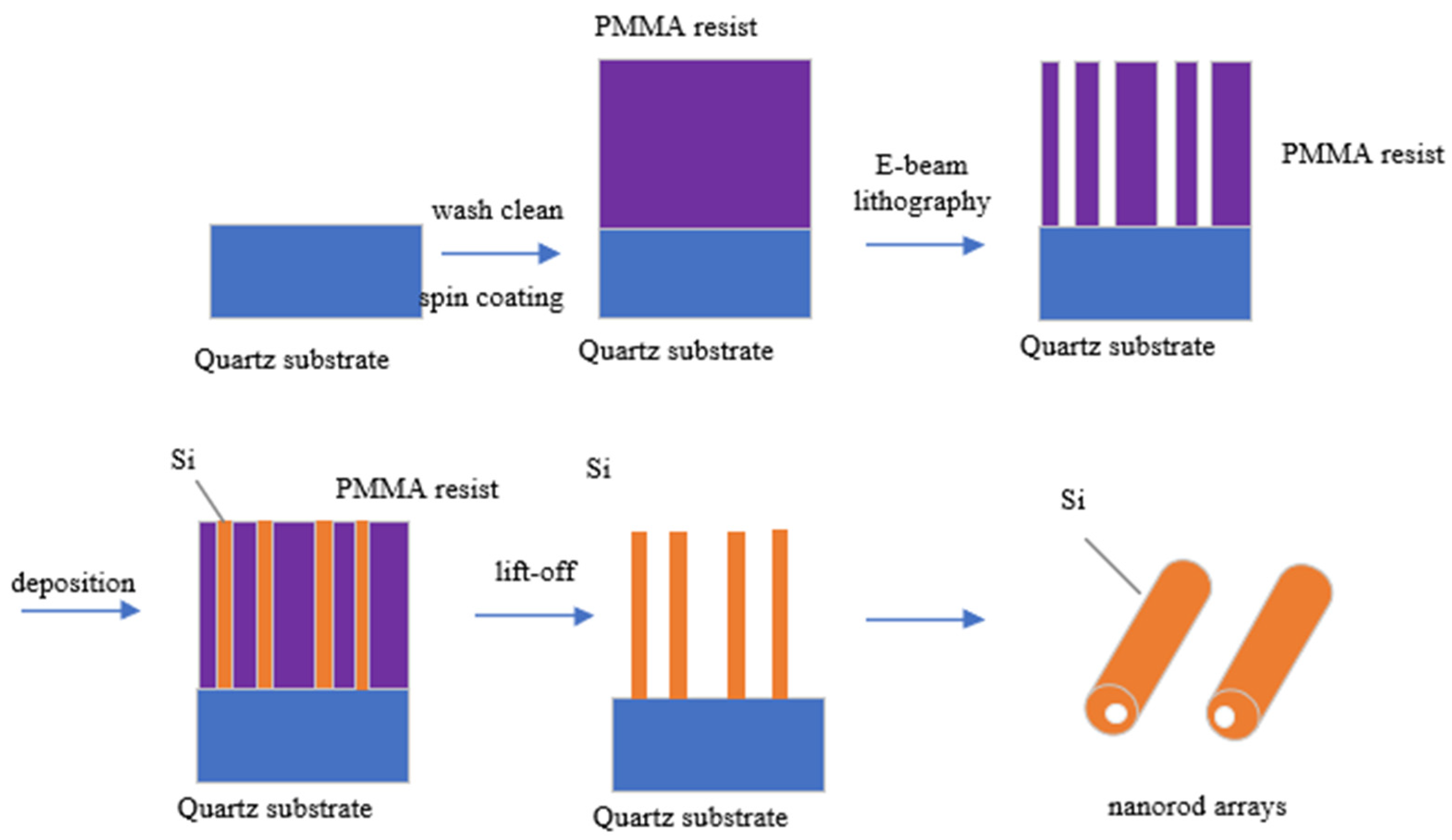
2. Structure and Theory

Figure 1 shows the schematic of the proposed optical sensor structures. Figure 1a shows the solid silicon nanorod array for comparison. Figure 1b gives the silicon nanorod of the air hole at the center, Figure 1c presents the holes which shift in the same direction, and Figure 1d shows the two adjacent holes which shift in the opposite direction. All the proposed nanostructures are entirely immersed in a liquid with a refractive index of 1.312. The refractive index of silicon is n s = 3.42.
The parameters of the sensor proposed in this paper are the following: the period of the rod array is P, the radius of the individual rod array is R, and the spacing between the two nanorods is D. The radius of the hole is r, and the offset of the hole to the center of the nanorod is d, which plays a crucial role in determining the Fano resonance line shape and the quality factor of the sensor. By varying these parameters, the properties of the sensor can be optimized to achieve high-quality factors and improve its performance in various applications. It was calculated that silicon has no absorption at the operating wavelength [38].
Sensitivity and FOM are commonly used to evaluate the performance of a sensor and can be expressed as [39]
S = Δ λ r e s / Δ n w ,
F O M = S / Δ λ ,
where Δ λ r e s is the resonance wavelength shift, Δ n w is the amount of n w variation, Δ λ is the full width at half maximum (FWHM) of resonance line-shape, and n w is the refractive index of the surrounding medium, which varies from 1.312 to 1.316.
All simulations are performed using the finite element method in COMSOL Multiphysics software. The two-dimensional structure is utilized, which is considered infinite in the x-direction and periodically aligned in the y-direction. The incident plane wave is set to propagate in the z-direction with an electric field parallel to the x-direction (transverse electric field, TE mode).

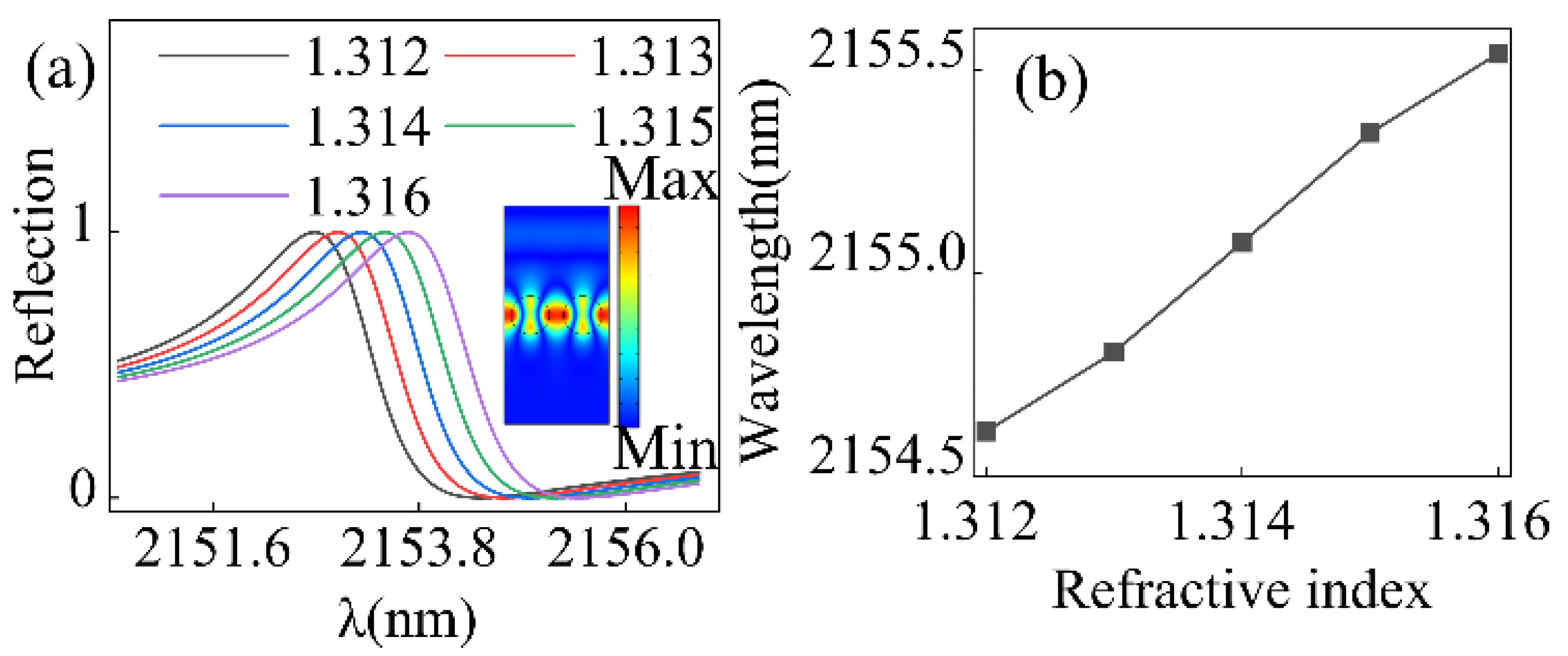
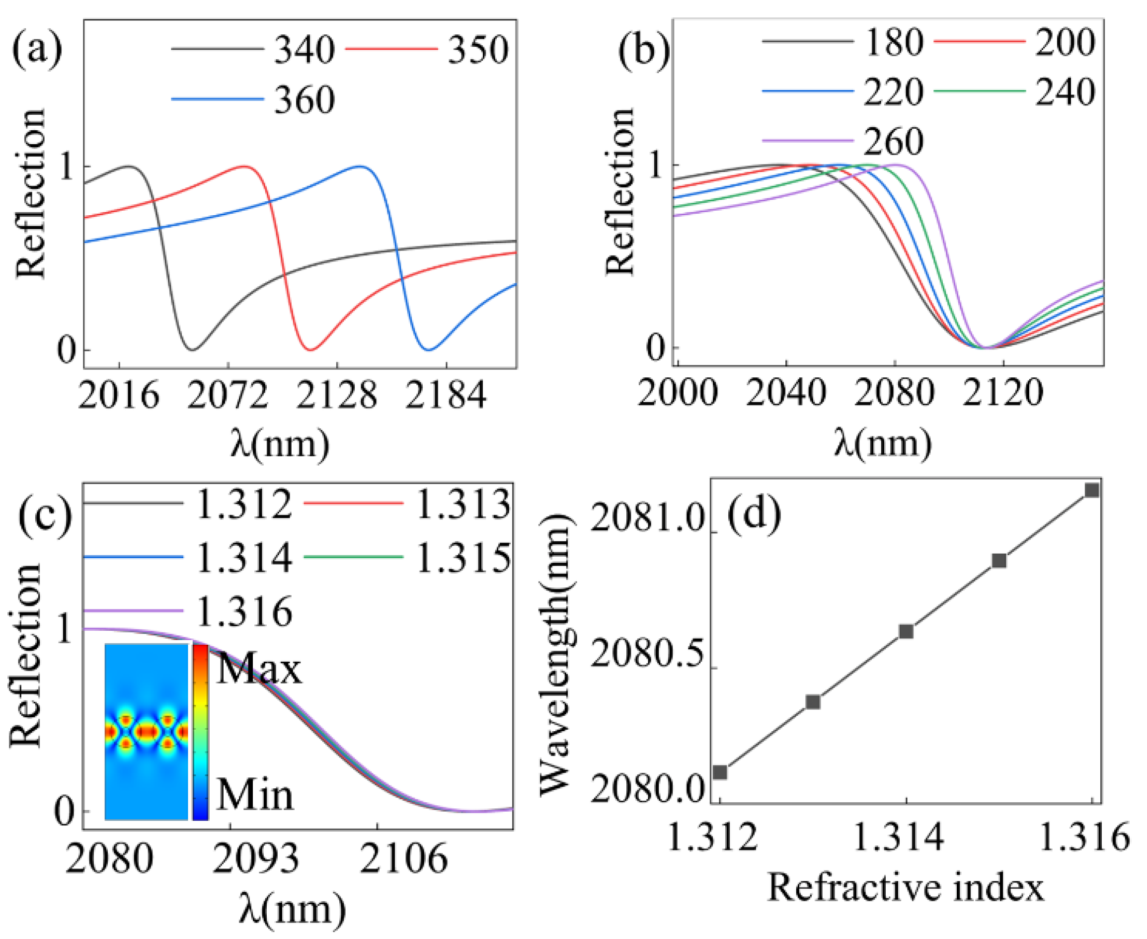
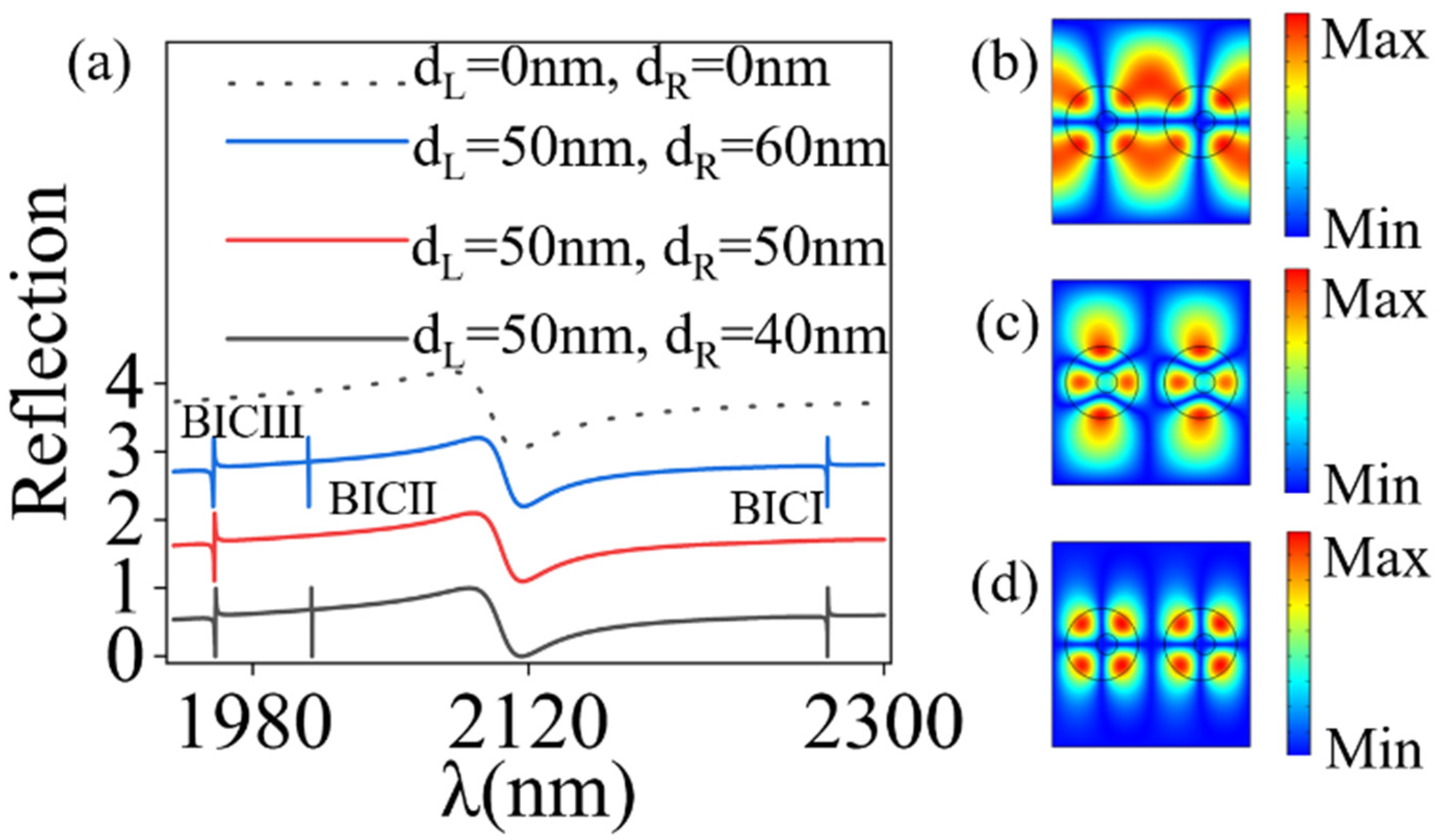
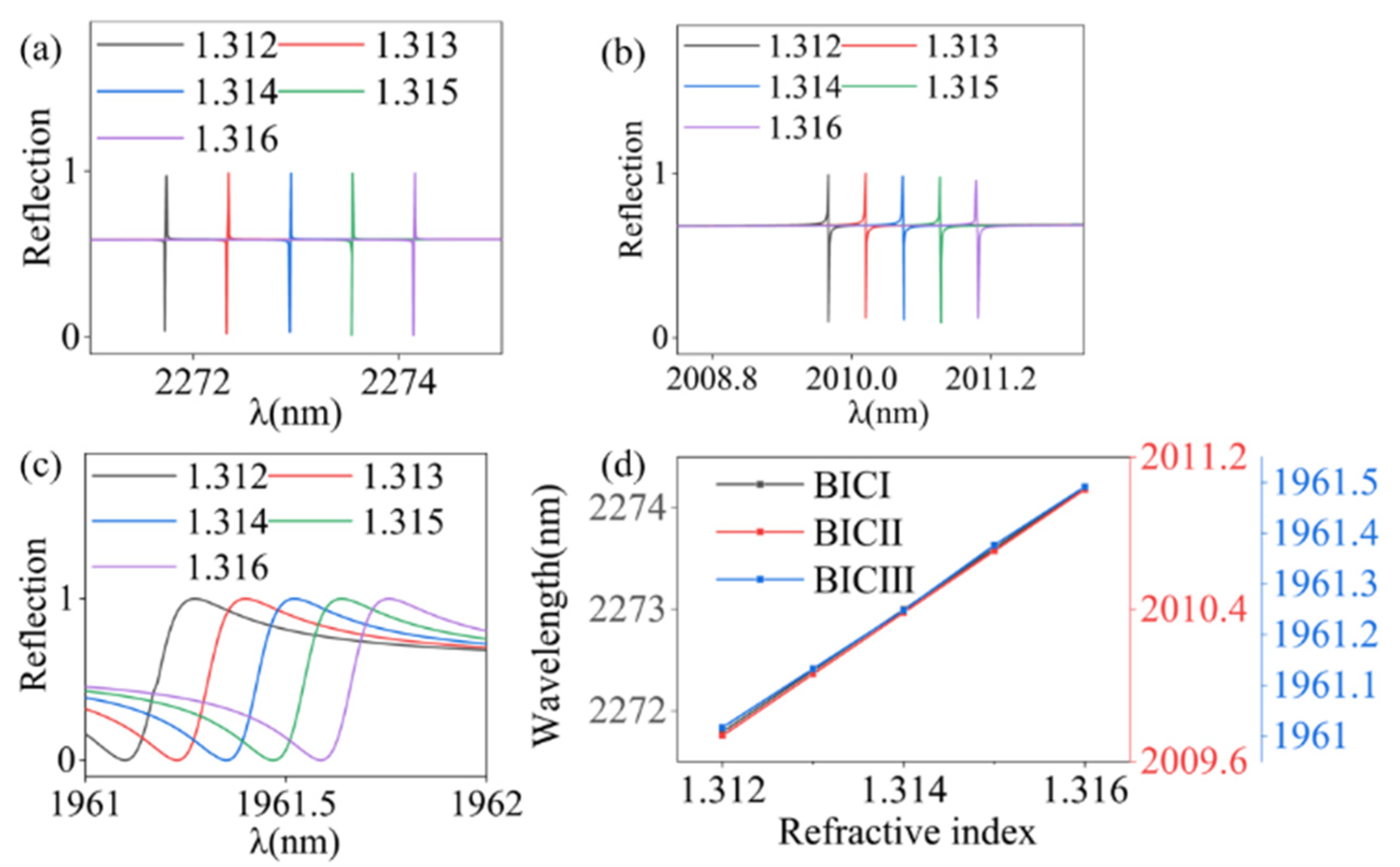
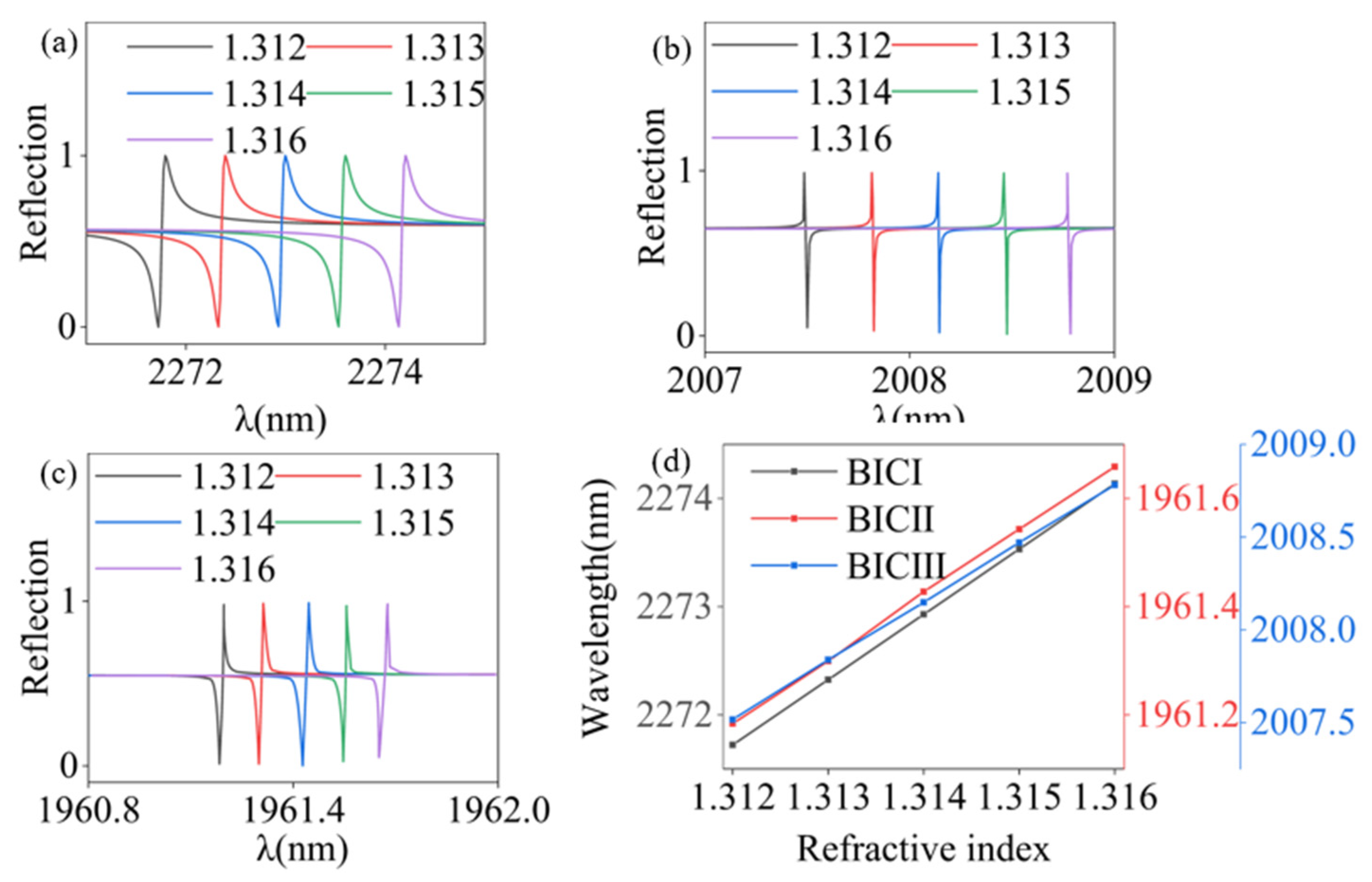
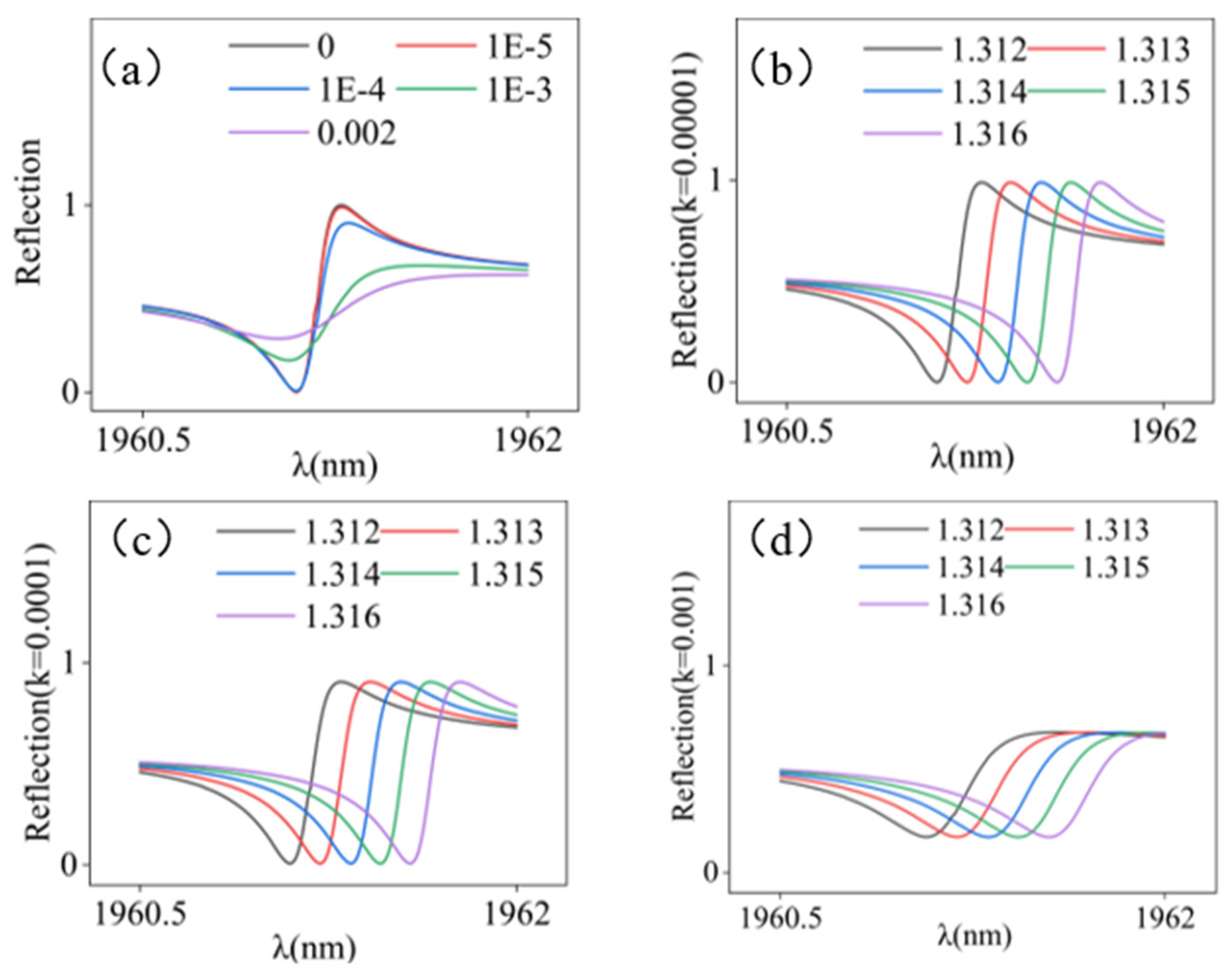
3. Results and Discussion

First, we calculated the reflectance spectra of the pristine rod arrays (R = 350 nm) without changing the external medium, as shown in Figure 2.
Figure 2a shows the reflectance spectra of a nanorod array at different refractive indices when the distance between the two nanorod widths is 260 nm (D = 260 nm), while the rod radius is 350 nm (R = 350 nm). The electric field at the resonance mode is shown in the inset. The field is concentrated in the gap between two nanorods. The resonance frequency has a redshift when the refractive index of the surrounding medium increases from 1.312 to 1.316, as shown in Figure 2b. The resonance peak shifts by 0.26 nm for the change in the refractive index of 0.001, with the sensitivity S = 263 nm/RIU. The FOM is calculated to be around 145. This result is even worse than the performance of some plasma metasurfaces. We have therefore made subsequent improvements.
The optical response in the nanorod array when the holes are introduced and placed at the center of nanorods (Figure 1b) is further studied, as shown in Figure 3, while we keep the holes of r = 100 nm and n 0 = 1 to test.
Figure 3a shows the reflectance spectrum of the nanorod array with a constant spacing of 260 nm and the same refractive index n w = 1.312, and Figure 3b presents the reflectance spectrum with varying nanorod array spacing while maintaining the same refractive index n w = 1.312 and nanorod radius R = 350 nm. We keep the nanorod array of R = 250 nm and D = 260 nm to test the sensing property, as shown in Figure 3c. The resonance peak shifts by 0.26 nm for a 0.001 change in the refractive index (as shown in Figure 3d). The sensitivity is S = 193 nm/RIU and the FOM = 5.7, with a resonance frequency of 2114 nm (Figure 1b). The resonance frequency has a redshift when the refractive index of the surrounding medium increases from 1.312 to 1.316 and the peaks or dips in the reflectance spectra shift towards larger wavelengths with the increases in the radius of the nanorod array. Similar to a resonant cavity, when the expansion of the radius of the nanorods can be seen as an increase in the proportion of the medium in a certain space, the air decreases, resulting in an increase in the relative refractive index; when the refractive index of the medium in the resonant cavity increases, the resonance frequency is affected. This is because the refractive index change changes the propagation speed of light waves in the cavity, and the resonant frequency is related to the propagation speed. The propagation speed of light in a medium can be described by the following equation: v = c/n, where v is the propagation speed of light in a medium, c is the speed of light in a vacuum, and n is the refractive index of the medium. The resonant frequency of the resonant cavity can be approximated by the following formula: f = c/(2L), where f is the resonant frequency, c is the speed of light in a vacuum, and L is the effective length of the resonant cavity. When the refractive index n of the medium increases, the propagation velocity v of light in the medium decreases because an increase in n means that the medium’s ability to refract light increases. According to the above equation, a decrease in the propagation velocity results in a decrease in the resonant frequency. When the radius increases, the effective length of the resonator increases, resulting in a decrease in the resonant frequency.
The results show that the performance of the sensor in the nanorod arrays with holes at the center was poorer than that in the solid nanorod array. Through previous experiments [40], we have found that breaking the symmetry of the nano-array structure can effectively improve the optical properties such as the sensitivity of the sensor [14].
The electric field distribution in the dielectric rods suggests that the waveguide modes are similar as a coupled analogue quadrupole system of systems. Thus, the output waves above and below the rod array have the same phase symmetry. This is related to the emergence of BIC [41]. Due to the coupling of the two nanorods, the left and right rods in the formed dimer are coupled in a dipole-quadrupole mode.
Next, we offset the holes to further study the optical responses. We first study the case when the holes shift to the same direct, i.e., two nanorods are considered as a group with the hole in the left rod shifting to the right direction of a constant value dL = 50 nm, while the hole in the right rod also shifts to the right direction of a value dR (Figure 1c).
Figure 4a shows the reflectance spectra in the nanorod arrays with different dR when the gap between two nanorods is 260 nm, and the radius of nanorod is 350 nm. For comparison, the reflectance spectra in the nanorod with the holes at the center are also shown in Figure 4a.
It is clear that a new resonance peak around 1960 nm appears in the reflectance spectrum when dR = dL = 50 nm. The peak originates from the shift of the hole from the center. That means that there is a BIC mode at such frequency when the holes are at the center of the nanorods. The shift breaks the symmetry of the nanostructure to give the quasi-BIC. It is interesting that there are two additional peaks occurring at around 2010 nm and 2273 nm when dRdL. That means that two additional BIC modes exist in the nanostructure with the holes at the center of the nanorods and turn into the quasi-BICs due to the further symmetry breaking. The electric field distributions at the quasi-BIC mode are shown in Figure 4b, c, and d, respectively. When the left hole is offset at 50 nm and the right hole is offset at 40 nm, the Q-factors are as follows: Q1 = 1.52 × 10⁴ (wavelength = 1960 nm), Q2 = 1.08 × 10⁶ (wavelength = 2010 nm), Q3 = 8 × 10 (wavelength = 2114 nm), and Q4 = 3.79 × 10⁶ (wavelength = 2273 nm). The optical performance of the structure is superior to that of nanorod arrays without holes or with holes only in the center.
The reflectance spectra around the three quasi-BICs in the nanostructure (R = 350 nm, D = 260 nm, r = 100 nm, dL = 50 nm, dR = 40 nm) under the different refractive indices of the surroundings are shown in Figure 5a–c.
The sensitivity and the FOM are calculated. For the first quasi-BIC mode, the resonance peak shifts by 0.6 nm for a 0.001 change in the refractive index. The sensitivity is S = 602.9 nm/RIU, and the FOM = 34977, with a resonance frequency of 2272 nm (Figure 5a). For the second quasi-BIC mode, the resonance frequency shifts by 0.023 nm for a 0.001 change in the refractive index, with a resonance frequency of 2009 nm. The sensitivity is S = 323.4 nm/RIU, and the FOM = 23900 (Figure 5b). For the third quasi-BIC mode, the resonance frequency shifts by 0.13 nm for a 0.001 change in the refractive index, with a resonance frequency of 2010 nm. The sensitivity is S = 118.96 nm/RIU, and the FOM = 700, with a resonance frequency of 1961.2 nm (Figure 5c).
We finally investigate the optical response in the last configuration when two adjacent holes shift in the opposite direction, i.e., two nanorods are considered as a group with the hole in the left rod shifting to the right direction at a constant value of dL = 50 nm, while the hole in the right rod shifts to the left direction of a value dR. (Figure 1d). The reflectance spectra in the nanorod arrays with different dR values (R = 350 nm, D = 260 nm, n w = 1.312, r = 50 nm) are shown in Figure 6a. The similar phenomena are obtained as those in the last configuration. The one quasi-BIC mode and three quasi-BIC modes are observed when dR = dL and dRdL, respectively. When the left hole offset at 50 nm and the right hole offset at 40 nm, the Q-factors are as follows: Q1 = 1.22 × 10⁶ (wavelength = 1960 nm), Q2 = 1.02 × 10⁶ (wavelength = 2010 nm), Q3 = 8 × 10 (wavelength = 2114 nm), Q4 = 3.25 × 10⁴ (wavelength = 2273 nm).
The electric field distributions are given in Figure 6b–d. Such quasi-BICs also originate from the symmetry breaking. The reflectance spectra around the three quasi-BICs in the nanostructure (R = 350 nm, D = 260 nm, r = 100 nm, dL = 50 nm, and dR = 40 nm) under the different refractive indices of the surroundings are shown in Figure 7a–c.
The sensitivity and the FOM are also analyzed. The S = 602.7 nm/RIU and FOM = 8744, S = 316.8 nm/RIU and FOM = 23,500, and S = 115.5 nm/RIU and FOM = 9269, are obtained for the first, second, and third quasi-BICs modes, respectively.
Overall, the maximum sensitivity S = 602.7 nm/RIU and FOM = 34,977 are simultaneously observed in the nanostructure when two adjacent nanorods are considered as a group with the hole shifting to the same direction but with different values. The comparison of the performance of our proposed nanostructure with the reported results shown in Table 1. Although the sensitivity of our proposed nanostructures is some lower than that reported in the other nanostructures of quasi-BICs [34,42,43], the FOM in our nanostructures is indeed ultrahigh. The results indicate that our proposed nanostructure can simultaneously give high sensitivity and FOM for high-performance sensors.
For the real surrounding medium, the extinction coefficient κ is probably not zero at the resonance wavelengths, e.g., the κ is around 10−5 or 10−6 for pentane, octane, methanol, ethanol, propanol, benzene, and toluene at 2 μm [47]. In order to investigate the influence of light absorption caused by surrounding medium on the reflection spectrum of the structure, different extinction coefficients (κ) are set in the nanostructure of the left hole offset at 50 nm and the right hole offset at 40 nm, respectively, as shown in Figure 8. The thickness of surrounding medium is assumed to be 2 μm to save the simulation time.
When the extinction coefficient κ = 10−5, the reflectance spectrum is almost over-lapped with that without the extinction coefficient, while the peak(dip) values decrease (increase) and the lineshapes become broader when the κ increases (Figure 8a). The resonance wavelengths are kept, and thus, the sensitivity is almost unchanged under the difference refractive index of the surrounding medium (Figure 8b–d). Even the thickness of the surrounding medium is 100 um (1 mm), the transmission is still around 99.4% (93.9%) as the κ = 10−5, and the Q-factor does not decrease too much, nor does the FOM.
Furthermore, it is possible to optimize the structure so that the resonance mode is in the wavelength region where the absorption of surrounding medium is neglected. The high sensitivity and FOM can both be kept.
Although this study is limited to the simulation level, the feasibility of the experiment is demonstrated in Figure 9 and Figure 10. BIC metasurfaces are usually prepared and processed using the electron beam exposure process, with the core equipment being an electron beam exposure machine (Electron Beam Lithography, EBL), which uses a vapor deposition process to prepare the etched metal mask. It is compatible with semiconductor micro-nanofabrication processes (lithography, etching, etc.) [48,49].
First, photoresist is spin-coated on a sufficiently cleaned quartz substrate, and after the photoresist is sufficiently cured, the PMMA nanoarray structure is obtained by electron beam lithography. Silicon is fully deposited in the PMMA nanorod arrays. The rest of the PMMA photoresist was then completely cleaned to obtain the silicon nanorod arrays.

4. Conclusions

In summary, we investigate the optical sensing in an all-dielectric nanorod array. The ultra-high sensitivity and FOM are observed in the designed nanostructure of two adjacent nanorods of holes shifting in the same direction but at different values. The maximum sensitivity and FOM reach up to 602.9 nm/RIU and FOM = 34,977. We believe that such proposed nanostructure has great potential applications as highly sensitive optical sensors.

Author Contributions

Y.Z., T.N. and Z.F. performed the theoretical analysis. Z.W. performed data measurement and analysis. All authors have read and agreed to the published version of the manuscript.

Funding

This work is supported by the National Natural Science Foundation of China (Nos. 42271093 and 12174228) and Natural Science Foundation of Shandong Province (No. ZR2020MA082).

Institutional Review Board Statement

Not applicable.

Informed Consent Statement

Not applicable.

Data Availability Statement

The data supporting the findings of this study are available from the corresponding authors upon reasonable request.

Conflicts of Interest

The authors declare no conflicts of interest.

References

  1. Kumar, S.; Singh, R. Recent optical sensing technologies for the detection of various biomolecules: Review. Opt. Laser Technol. 2021, 134, 106620. [Google Scholar] [CrossRef]
  2. Moreno, Y.; Song, G.; Xing, Z.; Sun, Y.; Yan, Z. Hybrid tilted fiber gratings-based surface plasmon resonance sensor and its application for hemoglobin detection. Chin. Opt. Lett. 2020, 18, 100601. [Google Scholar] [CrossRef]
  3. Sen, S.; Ahmed, K. Design of terahertz spectroscopy based optical sensor for chemical detection. SN Appl. Sci. 2019, 1, 1215. [Google Scholar] [CrossRef]
  4. Chocarro-Ruiz, B.; Fernandez-Gavela, A.; Herranz, S.; Lechuga, L. Nanophotonic label-free biosensors for environmental monitoring. Curr. Opin. Biotechnol. 2017, 45, 175–183. [Google Scholar] [CrossRef] [PubMed]
  5. Wang, X.; Deng, H.; Yuan, L. High sensitivity cascaded helicalcore fiber SPR sensors. Chin. Opt. Lett. 2021, 19, 091201. [Google Scholar] [CrossRef]
  6. Anker, J.; Hall, W.; Lyandres, O.; Shah, N.; Zhao, J.; Van Duyne, R. Biosensing with plasmonic nanosensors. Nat. Mater. 2008, 7, 442–453. [Google Scholar] [CrossRef] [PubMed]
  7. Monticone, F.; Alu, A. Metamaterial, plasmonic and nanophotonic devices. Rep. Prog. Phys. 2017, 80, 036401. [Google Scholar] [CrossRef] [PubMed]
  8. Wang, J.; Du, J. Plasmonic and Dielectric Metasurfaces: Design, Fabrication and Applications. Appl. Sci. 2016, 6, 239. [Google Scholar] [CrossRef]
  9. Tseng, M.; Fang, X.; Savinov, V.; Wu, P.; Ou, J.; Zheludev, N.; Tsai, D. Coherent selection of invisible high-order electromagnetic excitations. Sci. Rep. 2017, 7, 44488. [Google Scholar] [CrossRef]
  10. Yang, Y.; Kravchenko, I.; Briggs, D.; Valentine, J. All-dielectric metasurface analogue of electromagnetically induced transparency. Nat. Commun. 2014, 5, 5753. [Google Scholar] [CrossRef]
  11. Regmi, R.; Berthelot, J.; Winkler, P.; Mivelle, M.; Proust, J.; Bedu, F.; Ozerov, I.; Begou, T.; Lumeau, J.; Rigneault, H.; et al. All-Dielectric Silicon Nanogap Antennas To Enhance the Fluorescence of Single Molecules. Nano Lett. 2016, 16, 5143–5151. [Google Scholar] [CrossRef]
  12. Bontempi, N.; Chong, K.; Orton, H.; Staude, I.; Choi, D.; Alessandri, I.; Kivshar, Y.; Neshev, D. Highly sensitive biosensors based on all-dielectric nanoresonators. Nanoscale 2017, 9, 4972–4980. [Google Scholar] [CrossRef] [PubMed]
  13. Tseng, M.; Jahani, A.; Leitis, A.; Altug, H. Dielectric Metasurfaces Enabling Advanced Optical Biosensors. ACS Photonics 2018, 8, 47–60. [Google Scholar] [CrossRef]
  14. Huo, Y.; Zhang, X.; Yan, M.; Sun, K.; Jiang, S.; Ning, T.; Zhao, L. Highly-sensitive sensor based on toroidal dipole governed by bound state in the continuum in dielectric non-coaxial core-shell cylinder. Opt. Express 2022, 30, 19030–19041. [Google Scholar] [CrossRef] [PubMed]
  15. Friedrich, H.; Wintgen, D. Physical realization of bound states in the continuum. Phys. Rev. A 1985, 31, 3964–3966. [Google Scholar] [CrossRef]
  16. Friedrich, H.; Wintgen, D. Interfering resonances and bound states in the continuum. Phys. Rev. A 1985, 32, 3231–3242. [Google Scholar] [CrossRef] [PubMed]
  17. Bulgakov, E.; Sadreev, A. Bound states in the continuum in photonic waveguides inspired by defects. Phys. Rev. B 2008, 78, 075105. [Google Scholar] [CrossRef]
  18. Plotnik, Y.; Peleg, O.; Dreisow, F.; Heinrich, M.; Nolte, S.; Szameit, A.; Segev, M. Experimental Observation of Optical Bound States in the Continuum. Phys. Rev. Lett. 2011, 107, 183901. [Google Scholar] [CrossRef] [PubMed]
  19. Xiao, S.; Qin, M.; Duan, J.; Wu, F.; Liu, T. Polarization-controlled dynamically switchable high-harmonic generation from all-dielectric metasurfaces governed by dual bound states in the continuum. Phy. Rev. B 2022, 105, 195440. [Google Scholar] [CrossRef]
  20. Liu, D.; Yu, X.; Wu, F.; Du, W.; Chen, L.; Liu, F.; Kuwahara, M.; Ono, S. Terahertz asymmetric metallic hole arrays with polarization-independent quasi-bound states in the continuum for membrane sensing. Opt. Express 2023, 31, 23608–23620. [Google Scholar] [CrossRef]
  21. Ning, T.; Li, X.; Zhao, Y.; Yin, L.; Huo, Y.; Zhao, L.; Yue, Q. Giant enhancement of harmonic generation in all-dielectric resonant waveguide gratings of quasi-bound states in the continuum. Opt. Express 2020, 28, 34024–34034. [Google Scholar] [CrossRef] [PubMed]
  22. Koshelev, K.; Favraud, G.; Bogdanov, A.; Kivshar, Y.; Fratalocchi, A. Nonradiating photonics with resonant dielectric nanostructures. Nanophotonics 2019, 8, 725–745. [Google Scholar] [CrossRef]
  23. Wu, F.; Wu, J.; Guo, Z.; Jiang, H.; Sun, Y.; Li, Y.; Ren, J.; Chen, H. Giant Enhancement of the Goos-Hänchen Shift Assisted by Quasibound States in the Continuum. Phys. Rev. Appl. 2019, 12, 014028. [Google Scholar] [CrossRef]
  24. Li, W.; Liu, Y.; Ling, L.; Sheng, Z.; Cheng, S.; Yi, Z.; Wu, P.; Zeng, Q.; Tang, B.; Ahmad, S. The tunable absorber films of grating structure of AlCuFe quasicrystal with high Q and refractive index sensitivity. Surf. Interfaces 2024, 48, 104248. [Google Scholar] [CrossRef]
  25. Li, W.; Liu, M.; Cheng, S.; Zhang, H.; Yang, W.; Zao, Y.; Zeng, Q.; Tang, B.; Ahmad, S.; Sun, T. Polarization independent tunable bandwidth absorber based on single-layer graphene. Diam. Relat. Mater. 2024, 142, 110793. [Google Scholar] [CrossRef]
  26. Li, W.; Xu, F.; Cheng, S.; Yang, W.; Liu, B.; Liu, M.; Yi, Z.; Tang, B.; Chen, J.; Sun, T. Six-band rotationally symmetric tunable absorption film based on AlCuFe quasicrystals. Opt. Laser Technol. 2024, 169, 110186. [Google Scholar] [CrossRef]
  27. Li, Z.; Xiang, Y.; Xu, S.; Dai, X. Ultrasensitive terahertz sensing in all-dielectric asymmetric metasurfaces based on quasi-BIC. J. Opt. Soc. Am. B 2022, 39, 286–291. [Google Scholar] [CrossRef]
  28. Liu, W.; Yan, B.; Jiang, X. High performance sensor based on phase difference induced quasi-BIC and Fermi energy. Opt. Lett. 2023, 48, 6012–6014. [Google Scholar] [CrossRef] [PubMed]
  29. Samadi, M.; Abshari, F.; Algorri, J.; Varona, P.; Cobo, L.; Higuera, J.; Prna, J.; Zografopoulos, D.; Dell’Olio, F. All-Dielectric Metasurface Based on Complementary Split-Ring Resonators for Refractive Index Sensing. Photonics 2022, 9, 130. [Google Scholar] [CrossRef]
  30. Yu, S.; Wang, Y.; Gao, Z.; Li, H.; Song, S.; Yu, J.; Zhao, T. Dual-band polarization-insensitive toroidal dipole quasi-bound states in the continuum in a permittivity-asymmetric all-dielectric meta-surface. Opt. Express 2022, 30, 4084–4095. [Google Scholar] [CrossRef]
  31. Wang, T.; Liu, S.; Zhang, J.; Xu, L.; Yang, M.; Ma, D.; Jiang, S.; Jiao, Q.; Tan, X. Dual high-Q Fano resonances metasurfaces excited by asymmetric dielectric rods for refractive index sensing. Nanophotonics 2024, 13, 463–475. [Google Scholar] [CrossRef]
  32. Chen, H.; Fan, X.; Fang, W.; Cao, S.; Sun, Q.; Wang, D.; Niu, H.; Li, C.; Wei, X.; Bai, C.; et al. Investigation of Multiple High Quality-Factor Fano Resonances in Asymmetric Nanopillar Arrays for Optical Sensing. Photonics 2024, 11, 68. [Google Scholar] [CrossRef]
  33. Cao, S.; Fan, X.; Fang, W.; Chen, H.; Bai, C.; Tong, C. A high-performance multi-wavelength optical switch based on multiple Fano resonances in an all-dielectric metastructure. Optoelectron. Lett. 2024, 20, 193–199. [Google Scholar] [CrossRef]
  34. Sun, Q.; Fan, X.; Fang, W.; Chen, H.; Wang, D.; Cao, S.; Niu, H.; Li, C.; Bai, C.; Wei, X. High sensitivity multiple Fano resonances sensing in all-dielectric hollow nanocylinder dimer metastructure. Opt. Quant. Electron. 2024, 56, 337. [Google Scholar] [CrossRef]
  35. Chen, H.; Fan, X.; Fang, W.; Zhang, B.; Cao, S.; Sun, Q.; Wang, D.; Niu, H.; Li, C.; Wei, X.; et al. High-Q Fano resonances in all-dielectric metastructures for enhanced optical biosensing applications. Biomed. Opt. Express 2024, 15, 294–305. [Google Scholar] [CrossRef] [PubMed]
  36. Liang, S.; Xu, F.; Li, W.; Yang, W.; Cheng, S.; Yang, H.; Chen, J.; Yi, Z.; Jiang, P. Tunable smart mid infrared thermal control emitter based on phase change material VO2 thin film. Appl. Therm. Eng. 2023, 232, 121074. [Google Scholar] [CrossRef]
  37. Shangguan, Q.; Zhao, Y.; Song, Z.; Wang, J.; Yang, H.; Chen, J.; Liu, C.; Cheng, S.; Yang, W.; Yi, Z. High sensitivity active adjustable graphene absorber for refractive index sensing applications. Diam. Relat. Mater. 2022, 128, 109273. [Google Scholar] [CrossRef]
  38. Pierce, D.; Spicer, W. Electronic structure of amorphous Si from photoemission and optical studies. Phys. Rev. B 1972, 5, 3017–3029. [Google Scholar] [CrossRef]
  39. Zhao, X.; Zhang, X.; Zhu, X.; Shi, Y. Long-range surface plasmon resonance sensor based on the GK570/Ag coated hollow fiber with an asymmetric layer structure. Opt. Express 2019, 27, 9550–9560. [Google Scholar] [CrossRef]
  40. Zhao, C.; Huo, Y.; Liu, T.; Liao, Z.; Xu, C.; Zhang, T. All-dielectric metasurface with multiple Fano resonances supporting high-performance refractive index sensing. J. Opt. Soc. Am. B 2023, 41, 36. [Google Scholar] [CrossRef]
  41. Pu, M.; Song, M.; Yu, H.; Hu, C.; Wang, M.; Wu, X.; Luo, J.; Zhang, Z.; Luo, X. Fano resonance induced by mode coupling in all-dielectric nanorod array. Appl. Phys. Express 2014, 7, 032002. [Google Scholar] [CrossRef]
  42. Sun, W.; Liang, Z.; Shi, X.; Yang, F.; Dong, Y.; Dai, R.; Jia, Y.; Xin, W.; Hou, E.; Wu, Z. Potential of high Q dual band Mid-Infrared metasurfaces with Quasi-BIC for refractive index sensing. Opt. Laser Technol. 2024, 174, 110631. [Google Scholar] [CrossRef]
  43. Luo, M.; Zhou, Y.; Zhao, X.; Guo, Z.; Li, Y.; Wang, Q.; Liu, J.; Luo, W.; Shi, Y.; Liu, A.; et al. High-Sensitivity Optical Sensors Empowered by Quasi-Bound States in the Continuum in a Hybrid Metal–Dielectric Metasurface. ACS Nano 2024, 18, 6477–6486. [Google Scholar] [CrossRef]
  44. Lu, X.; Zheng, G.; Zhou, P. High performance refractive index sensor with stacked two-layer resonant waveguide gratings. Results Phys. 2019, 12, 759–765. [Google Scholar] [CrossRef]
  45. Shi, C.; Liu, X.; Hu, J.; Han, H.; Zhao, J. High performance optical sensor based on double compound symmetric gratings. Chin. Opt. Lett. 2022, 20, 021201. [Google Scholar] [CrossRef]
  46. Zhou, X.; Wang, Y.; Sun, Y.; Wang, F.; Yan, X.; Zhang, X.; Suzuki, T.; Ohishi, Y.; Cheng, T. High sensitivity and stability probe-type refractive index sensor based on an optical fiber metasurface. J. Opt. Soc. Am. B 2023, 40, 1945–1952. [Google Scholar] [CrossRef]
  47. Myers, T.; Tonkyn, R.; Danby, T.; Taubman, M.; Bernacki, B.; Birnbaum, J.; Sharpe, S.; Johnson, T. Accurate measurement of the optical constants n and k for a series of 57 inorganic and organic liquids for optical modeling and detection. Appl. Spectrosc. 2018, 72, 535–550. [Google Scholar] [CrossRef] [PubMed]
  48. Yoon, G.; Kim, I.; So, S.; Mun, J.; Kim, M.; Rho, J. Fabrication of three-dimensional suspended, interlayered and hierarchical nanostructures by accuracy-improved electron beam lithography overlay. Sci. Rep. 2017, 7, 6668. [Google Scholar] [CrossRef]
  49. Liu, Z.; Guo, T.; Tan, Q.; Hu, Z.; Sun, Y.; Fan, H.; Zhang, Z.; Jin, Y.; He, S. Phase Interrogation Sensor Based on All-Dielectric BIC Metasurface. Nano Lett. 2023, 23, 10441–10448. [Google Scholar] [CrossRef]
Figure 1. Schematic of: (a) solid silicon nanorod array; (b) nanorod array with holes at the center; (c) nanorod array with holes shifting in the same direction; (d) nanorod array with two adjacent holes shifting in the opposite direction to form a group. The incident plane wave is set as propagating along the z-direction, the electric field is parallel to the x-direction (transverse electric, TE mode) with an amplitude of 1, and the magnetic field is parallel to the y-direction.
Photonics 11 00503 g001
Figure 2. (a) Reflectance spectra of nanorod array with the surrounding medium of different refractive indices. The inset shows the norm of the electric field along z-direction at the resonance mode at n = 1.312. (b) Resonance wavelength changes with refractive index.
Photonics 11 00503 g002
Figure 3. Reflectance spectra in the nanostructures of different (a) radii (D = 260 nm) and (b) spacing (R = 350 nm). (c) Reflectance spectra at different refractive indices (R = 250 nm, D = 260 nm). The inset shows the norm of the electric field along the z-direction at the resonance mode at n = 1.312. (d) Resonance wavelength changes with refractive index.
Photonics 11 00503 g003
Figure 4. (a) The reflectance spectra in the nanostructures when the two holes shift in the same direction with the left hole offset at 50 nm and the right hole offset at different values (40 nm, 50 nm, and 60 nm) ( n w = 1.312, R = 350 nm, D = 260 nm, r = 100 nm). The norm of the electric field distribution along z-direction at the first (b), second (c), and third (d) quasi-BIC resonance wavelengths when the dR = 40 nm.
Photonics 11 00503 g004
Figure 5. Reflectance spectra around the first (a), second (b), and third (c) quasi-BICs at different refractive indices. (d) The three quasi-BICs’ resonance wavelengths change with refractive index.
Photonics 11 00503 g005
Figure 6. (a) The reflectance spectra in the nanostructures when the two holes shift in the opposite direction with the left hole of 50 nm right-offset and the right hole of different left-offset values (40 nm, 50 nm, and 60 nm) ( n w = 1.312, R = 350 nm, D = 260 nm, r = 100 nm). The norm of electric field distribution along the z-direction at the first (b), second (c), and third (d) quasi-BIC resonance wavelengths when the dR = 40 nm.
Photonics 11 00503 g006
Figure 7. Reflectance spectra around the first (a), second (b), and third (c) quasi-BICs at different refractive indices. (d) The three quasi-BICs’ resonance wavelengths change with refractive index.
Photonics 11 00503 g007
Figure 8. (a) Reflectance spectra of different extinction coefficients ( n w = 1.312, BIC III). (b) The reflectance spectra in the nanostructures when the two holes shift in the same direction with κ = 10−5. (c) The reflectance spectra in the nanostructures when the two holes shift in the same direction with κ = 10−4. (d) The reflectance spectra in the nanostructures when the two holes shift in the same direction with κ = 10−3.
Photonics 11 00503 g008
Figure 9. The diagram scheme of the process for fabricating the BIC nanorod array (y-direction section diagram).
Photonics 11 00503 g009
Figure 10. The diagram scheme of the process for fabricating the BIC nanorod array (z-direction section diagram).
Photonics 11 00503 g010
Table 1. Properties of BIC-based metasurface sensors.
StructureIndex Sensitivity (nm/RIU)Wavelength (nm)FOMReferences
Non-coaxial core-shell cylinder nanostructure342750–8801295[14]
All-dielectric hollow nanocylinder dimer metastructure8701000–1600600[34]
Silicon triangular-hole nanodisk array248 1100–15003815[40]
Four elliptical nanodisks and a circular nanodisk23076000–70001792[42]
Optical sensor composed of a hybrid cylindrical tetramer metasurface (HCTM)497.2600–950266.3[43]
Stacked two-layer resonant waveguide gratings497.83 ——551[44]
Double compound symmetric gratings472 ——31,467[45]
Probe-type sensor based on an optical fiber metasurface1415 600–1600——[46]
Symmetric nanorod arrays with center hole602.9 1900–230034977This work
Disclaimer/Publisher’s Note: The statements, opinions and data contained in all publications are solely those of the individual author(s) and contributor(s) and not of MDPI and/or the editor(s). MDPI and/or the editor(s) disclaim responsibility for any injury to people or property resulting from any ideas, methods, instructions or products referred to in the content.

