Article

High-Bandwidth Lumped Mach-Zehnder Modulators Based on Thin-Film Lithium Niobate

1
Microsystem Packaging Research Center, Institute of Microelectronics of The Chinese Academy of Sciences, Beijing 100029, China
2
University of Chinese Academy of Sciences, Beijing 100049, China
*
Authors to whom correspondence should be addressed.
Photonics 2024, 11(5), 399; https://doi.org/10.3390/photonics11050399
Submission received: 18 March 2024 / Revised: 7 April 2024 / Accepted: 9 April 2024 / Published: 25 April 2024
(This article belongs to the Section Optoelectronics and Optical Materials)

Abstract

:
Recently, lumped Mach-Zehnder Modulators (MZMs) have received renewed attention due to their potential for low power consumption and compact size. However, the practicality of lumped MZMs with conventional lumped electrodes (C−LEs) is limited by their lower electro−optical (EO) bandwidth. The reduction in EO bandwidth results from the inherent trade−off between EO bandwidth and half−wave voltage length product ( V π L ) within the C−LE architecture. This paper proposes a thin−film lithium niobate (TFLN)−based lumped MZM with capacitively−loaded lumped electrodes (CL−LEs). The purely linear EO effect of the LN eliminates the parasitic capacitance in the doped PN junction and enhances the EO bandwidth. Furthermore, the CL−LE structure can break the limitation between EO bandwidth and V π L inherent in the C−LE design. Simulations show the proposed device achieves a high EO bandwidth of 32.4 GHz and a low V π L of 1.15 V·cm. Due to the reduced capacitance and lower V π L , the power consumption of the device is as low as 0.1 pJ/bit. Simulation results indicate that the open−eye diagrams are achieved at 64 Gb/s for 1.5 mm TFLN lumped MZM, with an ER of 2.97 dB. Consequently, the proposed device architecture substantially enhances the performance of lumped MZMs, showing promise for application in short−reach optical interconnects within data centers.

1. Introduction

Electro−optical (EO) modulators, as the main hardware in optical communication networks, are required to meet the requirements of low power consumption, low cost, and compact footprint [1,2,3]. Among the various modulator designs explored, the Traveling Wave Electrode Mach-Zehnder Modulator (TWE−MZM) features high modulation rates and broad optical bandwidth [4]. Nonetheless, the large footprint and high power consumption of the TWE−MZM reduces the integration density and increases the device cost. In contrast, the Micro−Ring Modulator (MRM) offers a more compact size and consumes less power [5]. However, the MRM faces challenges due to its restricted optical bandwidth, which renders its resonance severely sensitive to temperature fluctuations [6,7]. Modulators based on photonic crystals [8] and Bragg gratings [9] have also been reported. However, their application is limited by narrow optical bandwidth and a high sensitivity to fabrication errors.
Recently, there has been a renewed focus on lumped MZMs due to their potential for low power consumption and compact size [10,11,12,13,14,15,16,17,18,19,20,21,22]. Compared to the TWE, lumped electrodes act as capacitive elements that only consume energy during signal conversion, thus reducing the power consumption of the device [1,10]. Lumped MZMs combine the wide optical bandwidth of a Mach-Zehnder interferometer (MZI) with the compactness and energy efficiency of a lumped electrode [11]. However, their lower EO bandwidth hinders the practicality of lumped MZMs with conventional lumped electrodes (C−LEs) [11,12,13,14,15]. This reduced EO bandwidth is attributed to the intrinsic trade−off between EO bandwidth and the half−wave voltage length product ( V π L ) in the C−LE configuration. This trade−off limits the performance improvement of the device. Additionally, the silicon−based lumped MZMs suffer from increased parasitic capacitance due to doped PN junctions, further reducing their EO bandwidth [11,12,13,14,15,16,17,18,19,20]. Various efforts have been taken to increase the EO bandwidth, including the adoption of low output impedance [12] or switched capacitor drive circuits [13], equalizers [14,15], and predistortion techniques [16]. However, these approaches introduce additional power consumption, complexity, and costs. The lumped MZM on a thin−film lithium niobate (TFLN) platform with capacitively−loaded lumped electrodes (CL−LEs) is a promising solution [22]. The purely linear EO effect of the LN eliminates the parasitic capacitance in the doped PN junction and enhances the EO bandwidth. Furthermore, the CL−LE structure can break the limitation between EO bandwidth and V π L inherent in the C−LE structure and enhance the device performance.
In this paper, we propose a TFLN lumped MZM with CL−LE. Simulation results show that the proposed device can achieve a high EO bandwidth of 32.4 GHz and a low V π L of 1.15 V·cm. This is attributed to the fact that the CL−LE structure breaks the trade−off between EO bandwidth and V π L . This work demonstrates an improvement in EO bandwidth for lumped MZMs. Thanks to the reduced capacitance and lower V π L , the device exhibits low power consumption at 0.1 pJ/bit. Simulation results show that the device exhibits modulation rates up to 64 Gbps. Consequently, the proposed device architecture substantially enhances the performance of lumped MZMs, showing promise for application in short−reach optical interconnects within data centers.

2. Device and Principle
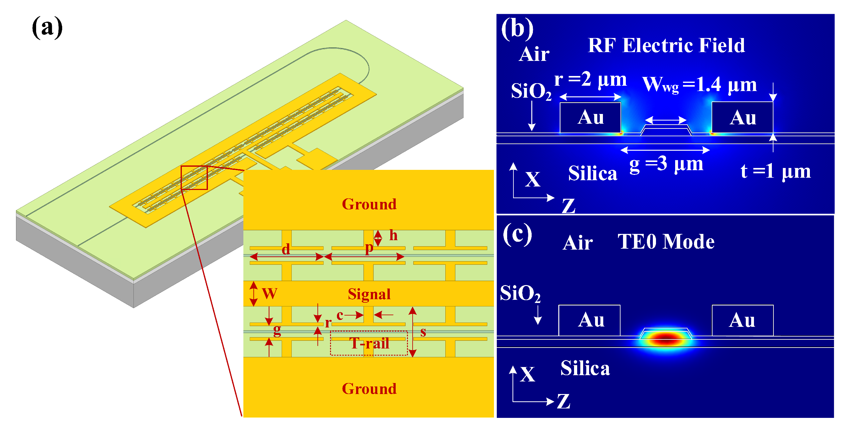
2.1. Device Layout

Figure 1a,b show the TFLN lumped MZM with C−LE structure and CL−LE structure, respectively. The modulator interfaces with an ultra−high numerical aperture (UHNA7) fiber, with a mode field diameter (MFD) of 3.2 μ m, through two LN edge couplers. A 1 × 2 multimode interferometer (MMI) ensures a 50:50 light splitting ratio. Light in the two modulation arms generates delayed and advanced phase shifts, resulting in intensity interference within the MMI. The proposed TFLN lumped MZM structure is based on X−cut LNOI wafers, which are characterized by a 600 nm thick LN layer on top and a 4.7 μ m thick oxygen−buried layer. The LNOI waveguide has a ridge width of 1.4 μ m, an etching depth of 0.3 μ m, and a bending radius of 125 μ m. The length of the device is 1.5 mm and the total length of the waveguide is 4 mm. Connection of the RF signal to the midpoint of the lumped electrode effectively halves the equivalent length and doubles the boundary frequency, as indicated by the formula: f = c/(4L n RF ) [1,13]. The effective refractive index n RF of the microwave signal in the LNOI modulator is 2.25 and the lumped electrode length L is 1.5 mm. This connection strategy increases the boundary frequency from 22.2 GHz to 44.4 GHz.

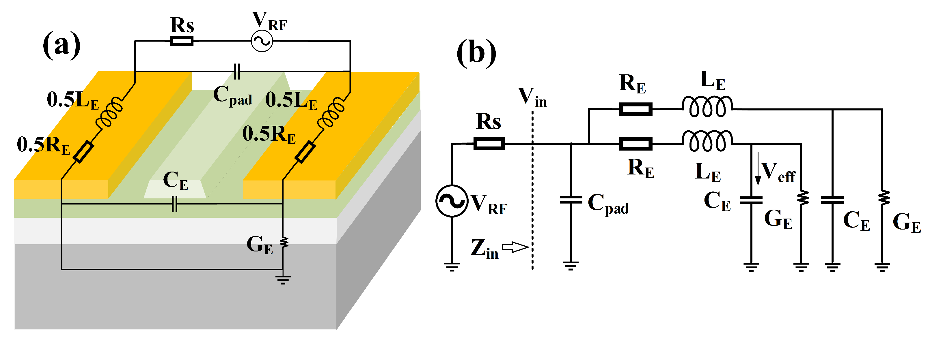
2.2. Theoretical EO Response

2.2.1. Electrical Cutoff Frequency

Generally, the EO bandwidth of lumped MZM is limited by the optical transit time and the RC constant of the device [10,12,21]. These two limitations are described separately below. Frequency−related variations in the parasitic parameters of devices cause a decrease in capacitor voltage, thereby limiting the EO bandwidth of the device. Figure 2a illustrates the configuration for driving a single arm of the lumped modulator. Figure 2b shows the Resistor−Inductor−Capacitor (RLC) equivalent circuit schematic. As shown in Figure 2b, feeding the RF signal from the center of the lumped electrodes effectively parallels two open transmission lines to the signal source. R E , L E , G E , and C E represent the resistance, inductance, conductance, and capacitance of the lumped electrodes, respectively. Meanwhile, R S and C pad represent the internal resistance of the signal source and the parasitic capacitance of the electrode pad, respectively. The RLGC parameters of the lumped electrode can be determined from the simulated S−parameters using the described method in [23]. Furthermore, C pad can be obtained from numerical software.
We evaluate the changes in the effective voltage ( V eff ) across the capacitor, which influences the phase shift. The V eff / V RF ratio indicates the voltage transfer efficiency, with its frequency dependence illustrating the EO response due to the RC constant. The calculation results are shown in Figure 3a. The EO bandwidths, limited by the RC constant, are 17 GHz and 13 GHz for device lengths of 1.5 mm and 2 mm, respectively.

2.2.2. Optical Transit Time

Optical transit time is another factor limiting the EO bandwidth of lumped MZMs, due to the finite transit time of light from input to output, which cannot instantaneously respond to RF signal changes [12]. We assume that a voltage with a swing of V RF is applied to the lumped electrodes, which can be expressed by V RF e j ω RF t , where t denotes the time and ω RF denotes the modulating signal angular frequency. The frequency−dependent phase shift is given by:
Δ φ ( ω RF ) Δ φ ( 0 ) = 1 τ 0 0 τ 0 e j ω RF t d t
where τ 0 denotes the time required for optical transit through the length of the device, given by τ 0 = L n g / c . L, n g , and c are the device length, the refractive index of the optical group, and the speed of light, respectively. According to the definition of EO bandwidth [24], the EO bandwidth influenced by the optical transit time can be expressed as:
S 21 op ( ω RF ) = 20 log 10 e j w RF τ 0 1 j w RF τ 0
The calculation results are shown in Figure 3b. For device lengths of 1.5 mm and 2 mm, the optical transit time limited EO bandwidths are 40 GHz and 30 GHz, respectively. The EO bandwidth, which accounts both the optical transit time and the RC constant, is illustrated by the dashed line in Figure 3b. The EO bandwidths for the 1.5 mm and 2 mm devices are 16 GHz and 12 GHz, respectively. Therefore, the simulation results show that the EO bandwidth is mainly limited by the RC constant.

2.2.3. Model Validation

To verify the accuracy of the model, we designed and fabricated a 2 mm long TFLN lumped MZM. The test results for the EO bandwidth of the device are shown in Figure 4, indicating a tested 3 dB EO bandwidth of 11 GHz. In Figure 4, the orange line depicts the calculated value for the EO model, demonstrating a 3 dB EO bandwidth of 12 GHz. The agreement between experimental results and theoretical calculations confirms the accuracy of the EO model. Therefore, we can use the EO model to qualitatively characterize the EO response of TFLN lumped MZMs.

3. EO Bandwidth Enhancement

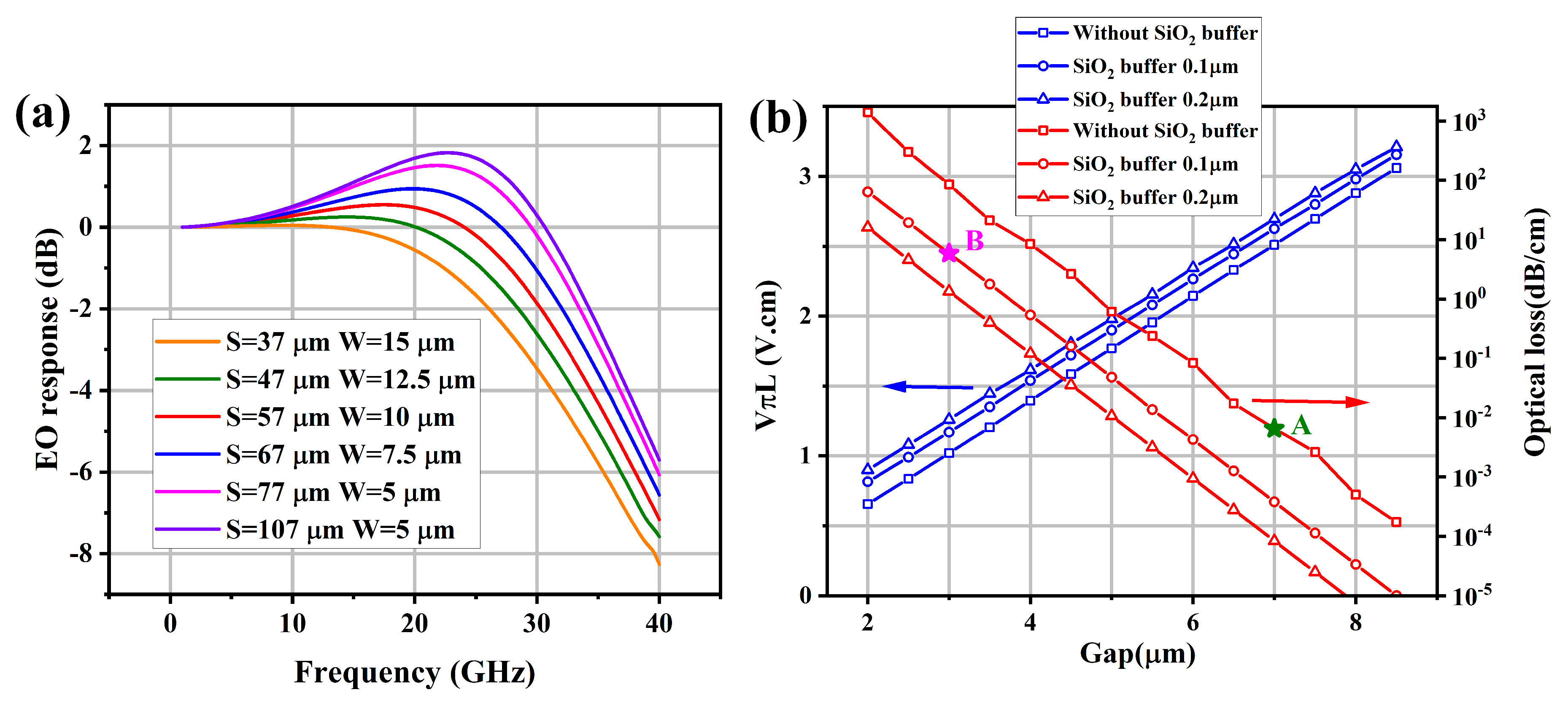
3.1. Limitations of Conventional Lumped Electrodes

In recent years, various efforts have been taken to improve the EO bandwidth of lumped MZMs. These efforts can be divided into several main categories. Firstly, the EO bandwidth can be increased by employing low output impedance drive circuits [12] or switched capacitor drive circuits [13]. However, achieving low output impedance in driver circuits presents significant complexity and challenges. In switched capacitor drive circuits, series capacitors reduce voltage across the modulator electrodes. Secondly, incorporating a terminating resistor can alleviate the rapidly decreasing frequency response of the capacitor at low frequencies, thus extending the EO bandwidth [12,17]. However, parallel resistors decrease the input impedance and reduce the electrode voltage. Lastly, implementing predistortion techniques [16] or RC equalizers [14,15] can also improve the EO bandwidth of the device. However, these approaches introduce additional power consumption, complexity, and costs. Therefore, optimizing the design of lumped MZMs to increase the EO bandwidth presents advantages such as simplicity, cost−effectiveness, and reduced power consumption compared to the above techniques.
The design optimization of the lumped MZM mainly involves RLGC parameters. Typically, the EO bandwidth is minimally influenced by resistance and conductance. Consequently, our study focuses primarily on the impact of inductance and capacitance on the EO bandwidth. Figure 5a illustrates the relationship between the capacitance per unit length and the EO response. Simulation results indicate that lower capacitance enhances the LC series resonance effect, thereby increasing the EO bandwidth. Consequently, the EO bandwidth increases from 11.8 GHz to 39 GHz as capacitance decreases from 150 pF/m to 15 pF/m. Figure 5b illustrates the relationship between inductance per unit length and the EO response. Simulation results indicate that increased inductance enhances the LC series resonance effect, enhancing the high−frequency component of the EO response, which in turn expands the EO bandwidth. Therefore, increasing the inductance from 300 nH/m to 800 nH/m enhances EO bandwidth from 12 GHz to 14 GHz. However, a further increase in inductance from 800 nH/m to 1200 nH/m slightly reduces the EO bandwidth. The reduction is attributed to the LC resonance frequency falling below the RC cutoff frequency, which constricts the EO bandwidth.
The above analysis indicates that reducing the capacitance and appropriately increasing the inductance of the modulator can improve the EO bandwidth. In practical designs, the structural parameters of modulator electrodes influence the parasitic capacitance and inductance. In a Ground−Signal−Ground (GSG) configuration, lumped electrodes can be modeled as two parallel metallic conductors. Their inductance and capacitance can be derived using the equations below [16]:
C = ϵ 0 ε r S 4 π k d × l
L = μ 0 l 2 π l n d w + t + 3 2
where ε 0 , μ 0 , and ε r denote the permittivity in vacuum, the magnetic permeability in vacuum, and the relative permittivity of the medium, respectively. S, d, L, w, and t correspond to the GSG electrode relative area, electrode gap, device length, signal electrode width, and electrode thickness, respectively. Equations (3) and (4) illustrate that expanding the electrode gap and narrowing the electrode width leads to higher inductance and lower capacitance. These adjustments favor the expansion of the EO bandwidth.
Figure 6a presents a TFLN lumped MZM with a C−LE. The insets illustrate the optical mode and RF electric field distributions across the cross−section of the modulation arm, respectively. Figure 6c,d show the signal electrode width and electrode gap versus capacitance and inductance per unit length for the C−LE configuration, respectively. When increasing the electrode gap from 2 μ m to 10 μ m, the capacitance decreases from 263 pF/m to 116 pF/m and the inductance increases from 298 nH/m to 471 nH/m. Concurrently, the EO bandwidth increases from 6.3 GHz to 15.9 GHz, which is consistent with the conclusions drawn from Equations (3) and (4). However, the electrode gap also affects the V π L , requiring a trade−off between EO bandwidth and V π L . Figure 6b shows that an increased electrode gap results in a higher V π L . Therefore, to balance V π L and EO bandwidth, the electrode gap must not be excessively large. The designed device has an electrode gap of 7 μ m and a signal electrode width of 10 μ m, marked with a white cross in Figure 6. Simulations reveal that for the 2 mm device, the EO bandwidth and V π L are 13.6 GHz and 2.56 V·cm, respectively. The relatively large capacitance ( 0.3 pF) introduced by the electrodes results in a lower EO bandwidth [22]. Therefore, TFLN lumped MZMs with C−LE structure encounter an intrinsic trade−off between EO bandwidth and V π L , which constrains enhancements in the EO bandwidth.

3.2. Capacitively−Loaded Lumped Electrodes

It is crucial to design an electrode structure that minimizes the capacitance of the device while preserving a low V π L , thereby breaking the trade−off between V π L and EO bandwidth [25,26,27,28,29]. The CL−LE structure, illustrated in Figure 7a, offers a promising solution. In the CL−LE structure, capacitance is primarily determined by the gap between the wide, unloaded electrodes without T−rails, whereas V π L depends on the gap between the T−rails [26]. Therefore, it is feasible to enlarge the gap between the unloaded electrodes while keeping the gap between the T−rails constant. This approach allows for preserving a low V π L while reducing the capacitance of the device.
Figure 8d,e depict the correlation between the unloaded electrode gap (S) and the unloaded signal electrode width (W) with the capacitance and inductance per unit length of the device, respectively, when the CL−LE structure is employed. Simulation results show that when S is extended from 17 μ m to 107 μ m, the capacitance decreases from 86.8 pF/m to 64.9 pF/m, and the inductance increases from 532 nH/m to 878 nH/m. Concurrently, the EO bandwidth increases from 28.1 GHz to 33.1 GHz at a device length of 1.5 mm, as shown in Figure 8f. Moreover, maintaining a constant gap between the T−rails ensures a low V π L for the device. Table 1 presents the parameters of the designed TFLN lumped MZM using the CL−LE structure, marked by a white cross in Figure 8. In the design of the CL−LE structure, we avoided selecting the maximum electrode spacing (S) and the minimum signal electrode width (W). This decision was made because such parameter combinations would lead to a significant overshoot in the EO response curve, as depicted in Figure 9a, distorting the signal. Considering the EO bandwidth and signal quality, we chose electrode spacings (S) of 57 μ m and signal electrode widths (W) of 10 μ m. To minimize the V π L of the device, the gap between T−rails was chosen to be 3 μ m. A 100 nm thick silica buffer layer was used to reduce the ohmic absorption loss of light by the metal as shown in Figure 9b. At this configuration, ohmic absorption loss drops to 3.96 dB/cm. Nevertheless, given the relatively short modulation region ( 1.5 mm), the incremental increase in ohmic absorption loss is a minimal 0.6 dB. To reduce the capacitance of the device, the electrodes were not covered with silica cladding [27]. Figure 8a,b compare the capacitance and inductance per unit length for the C−LE and CL−LE structures, respectively. Simulation results show that the CL−LE structure can greatly reduce the capacitance of the device. Figure 8c shows that the EO bandwidth can be increased from 13.6 GHz to 24.5 GHz by using a CL−LE structure at a device length of 2 mm. Furthermore, the EO bandwidth can be increased to 32.4 GHz when the device length is 1.5 mm. Additionally, the smaller gap between T−rails results in a lower V π L of 1.15 V·cm for the device. Therefore, the EO bandwidth can be significantly increased and the V π L reduced by utilizing the CL−LE structure. This is attributed to the fact that the CL−LE structure breaks the trade−off between EO bandwidth and V π L . Notably, integrating the CL−LE structure into the lumped MZMs aims to achieve both reduced capacitance and enhanced modulation efficiency. However, the introduction of the CL−TWE structure into the LN TWE−MZM aims to minimize microwave losses and preserve high modulation efficiency [25,26,27,28,29]. There is a difference in principle between them.

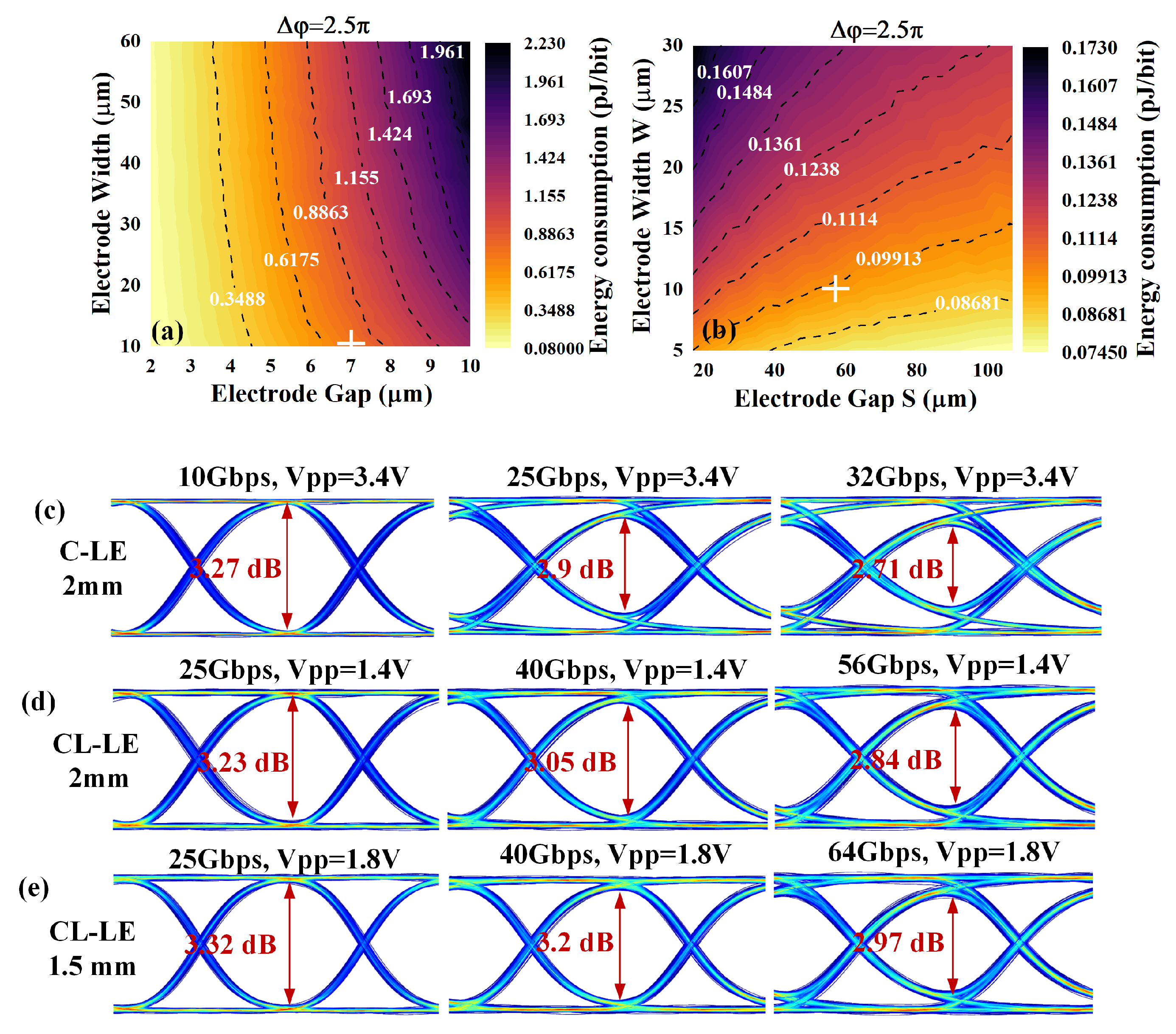
3.3. Energy Consumption and Eye Diagrams

The lumped electrodes can be viewed as a capacitive device that consumes energy only during signal conversion. The energy consumption per bit E lumped of the lumped modulator can be calculated using the following equation [11]:
E lumped = C V p p 2 M 2 l o g 2 M i = 0 M 1 M i i M 1 2
where C represents the capacitance of the device and M represents the modulation order.
Figure 10a shows the calculated E lumped of the TFLN lumped MZM with C−LE structure when the phase difference is 2.5 π (ER∼3.5 dB). While expanding the electrode gap decreases capacitance, the increase in voltage leads to a quadratic increase in power consumption. Therefore, a wider electrode gap results in higher energy consumption. With an electrode gap of 7 μ m and a signal electrode width of 10 μ m, the E lumped is 0.72 pJ/bit. Figure 9b shows the E lumped of TFLN lumped MZMs with CL−LE structure. Thanks to the lower capacitance and reduced V π L , the E lumped of the CL−LE structure is significantly lower than that of the C−LE structure. The TFLN lumped MZM designed with the CL−LE structure achieves a E lumped of 0.1 pJ/bit. The adoption of a segmented lumped modulating structure can further decrease E lumped while maintaining high bandwidth [30,31].
We characterize the large−signal properties of the TFLN lumped MZM. Figure 10 presents simulated eye diagrams for TFLN lumped MZMs featuring different electrode configurations. Pseudo−random sequences are used as modulation signals with a pattern length of 2 15 1 . ASE noise and random jitter have been added to the RF signals to simulate practical modulated waveforms. Here, the ASE features a power spectral density of 1 × 10 13 W/Hz, and the random jitter exhibits an amplitude of 0.02 unit intervals (UI) [32]. A continuous wave laser is used as the light source with a linewidth of 2 MHz, a power of 14 dBm, and a wavelength of 1550 nm. The PIN detector is characterized by a responsivity of 0.6 A/W, dark current of 5 nA, and thermal noise of 1 E 22 A / Hz 0.5 . The RC frequency response and optical transmission time effects are modeled by an RC low−pass filter and a fourth−order Bessel filter, respectively [16]. Figure 10c presents the simulated eye diagram for a 2 mm long TFLN lumped MZM with a C−LE structure. Simulation results show clear eye diagrams at 10 Gbps and 25 Gbps rates with extinction ratios of 3.27 dB and 2.9 dB, respectively. The eye diagram at 25 Gbps shows slight degradation consistent with the modeled EO bandwidth analysis (∼13.6 GHz). Figure 10d demonstrates that a TFLN MZM of the same length, utilizing a CL−LE structure, achieves a higher transmission rate. The eye diagram remains open up to 56 Gbps, with an extinction ratio of 2.84 dB. For a 1.5 mm long device, the eye can stay open for up to 64 Gbps with an extinction ratio of 2.97 dB. Therefore, the TFLN lumped MZM with a CL−LE structure offers superior eye quality and reduced energy consumption.

4. Discussion

Table 2 summarizes the currently reported performance parameters of lumped MZMs on silicon and TFLN platforms, including our research. Compared with previously reported devices, our proposed device eliminates the parasitic capacitance due to the doped PN junction. In addition, the CL−LE structure minimizes the device capacitance while maintaining a low V π L , thus breaking the trade−off between V π L and EO bandwidth. As a result, the device achieves a high EO bandwidth of 32.4 GHz and a low V π L of 1.15 V·cm. Due to the reduced capacitance and lower V π L , the power consumption of the device is as low as 0.1 pJ/bit. Thus, the proposed device structure greatly improves the performance of lumped MZM in terms of EO bandwidth, V π L , and power consumption. Finally, it is feasible to use a segmented lumped modulator structure to further reduce the power consumption while maintaining a high EO bandwidth.

5. Conclusions

In this paper, we propose a novel TFLN lumped MZM featuring CL−LE structure. Simulation results demonstrate that the device achieves a high EO bandwidth of 32.4 GHz and a low V π L of 1.15 V·cm. This is attributed to the CL−LE structure breaking the inherent trade−off between V π L and EO bandwidth of the C−LE. Thanks to the reduced capacitance and lower V π L , the device exhibits low power consumption at 0.1 pJ/bit. Furthermore, simulation results indicate the device achieves an open eye diagram at a data rate of 64 Gbps and an extinction ratio of 2.97 dB. Consequently, the proposed device architecture substantially enhances the performance of lumped MZMs, showing promise for application in short−reach optical interconnects within data centers.

Author Contributions

P.Y.: conceptualization, methodology, software, investigation, formal analysis, and writing—original draft; S.S.: conceptualization, methodology, software, and writing—review and editing; Y.Z.: data curation and writing—original draft; R.C.: visualization and investigation; H.H.: resources and supervision; H.X.: software and validation; F.L.: conceptualization, resources, supervision, and writing—review and editing. All authors have read and agreed to the published version of the manuscript.

Funding

This research received no external funding.

Institutional Review Board Statement

Not applicable.

Informed Consent Statement

Not applicable.

Data Availability Statement

Data are contained within the article.

Conflicts of Interest

The authors declare no conflicts of interest.

References

  1. Witzens, J. High-speed silicon photonics modulators. Proc. IEEE 2018, 106, 2158–2182. [Google Scholar] [CrossRef]
  2. Rao, A.; Fathpour, S. Compact lithium niobate electrooptic modulators. IEEE J. Sel. Top. Quantum Electron. 2017, 24, 1–14. [Google Scholar] [CrossRef]
  3. Zhang, M.; Wang, C.; Kharel, P.; Zhu, D.; Lončar, M. Integrated lithium niobate electro-optic modulators: When performance meets scalability. Optica 2021, 8, 652–667. [Google Scholar] [CrossRef]
  4. Wang, C.; Zhang, M.; Chen, X.; Bertrand, M.; Shams-Ansari, A.; Chandrasekhar, S.; Winzer, P.; Lončar, M. Integrated lithium niobate electro-optic modulators operating at CMOS-compatible voltages. Nature 2018, 562, 101–104. [Google Scholar] [CrossRef] [PubMed]
  5. Bahadori, M.; Yang, Y.; Hassanien, A.E.; Goddard, L.L.; Gong, S. Ultra-efficient and fully isotropic monolithic microring modulators in a thin-film lithium niobate photonics platform. Opt. Express 2020, 28, 29644–29661. [Google Scholar] [CrossRef] [PubMed]
  6. Sun, J.; Kumar, R.; Sakib, M.; Driscoll, J.B.; Jayatilleka, H.; Rong, H. A 128 Gb/s PAM4 silicon microring modulator with integrated thermo-optic resonance tuning. J. Light. Technol. 2018, 37, 110–115. [Google Scholar] [CrossRef]
  7. Bogaerts, W.; De Heyn, P.; Van Vaerenbergh, T.; De Vos, K.; Kumar Selvaraja, S.; Claes, T.; Dumon, P.; Bienstman, P.; Van Thourhout, D.; Baets, R. Silicon microring resonators. Laser Photonics Rev. 2012, 6, 47–73. [Google Scholar] [CrossRef]
  8. Li, M.; Ling, J.; He, Y.; Javid, U.A.; Xue, S.; Lin, Q. Lithium niobate photonic-crystal electro-optic modulator. Nat. Commun. 2020, 11, 4123. [Google Scholar] [CrossRef] [PubMed]
  9. Pohl, D.; Messner, A.; Kaufmann, F.; Escalé, M.R.; Holzer, J.; Leuthold, J.; Grange, R. 100-GBd waveguide Bragg grating modulator in thin-film lithium niobate. IEEE Photonics Technol. Lett. 2020, 33, 85–88. [Google Scholar] [CrossRef]
  10. Li, X.; Yang, F.; Zhong, F.; Deng, Q.; Michel, J.; Zhou, Z. Single-drive high-speed lumped depletion-type modulators toward 10 fJ/bit energy consumption. Photonics Res. 2017, 5, 134–142. [Google Scholar] [CrossRef]
  11. Mao, D.; Alam, M.S.; Parvizi, M.; El-Fiky, E.; Abdo, A.; Ben-Hamida, N.; Plant, D.V. Design, analysis, and characterization of a compact silicon photonic modulator with meandered phase shifters. Opt. Express 2022, 30, 32990–33002. [Google Scholar] [CrossRef] [PubMed]
  12. Azadeh, S.S.; Nojić, J.; Moscoso-Mártir, A.; Merget, F.; Witzens, J. Power-efficient lumped-element meandered silicon Mach-Zehnder modulators. In Proceedings of the Silicon Photonics XV, SPIE, Bellingham, WA, USA, 26 February 2020; Volume 11285, pp. 65–75. [Google Scholar]
  13. Zhou, S.; Wu, H.T.; Sadeghipour, K.; Scarcella, C.; Eason, C.; Rensing, M.; Power, M.J.; Antony, C.; O’Brien, P.; Townsend, P.D.; et al. Optimization of PAM-4 transmitters based on lumped silicon photonic MZMs for high-speed short-reach optical links. Opt. Express 2017, 25, 4312–4325. [Google Scholar] [CrossRef] [PubMed]
  14. Sobu, Y.; Tanaka, S.; Tanaka, Y. High-speed-operation of all-silicon lumped-electrode modulator integrated with passive equalizer. Ieice Trans. Electron. 2020, 103, 619–626. [Google Scholar] [CrossRef]
  15. Tanaka, S.; Simoyama, T.; Aoki, T.; Mori, T.; Sekiguchi, S.; Jeong, S.H.; Usuki, T.; Tanaka, Y.; Morito, K. Ultralow-power (1.59 mW/Gbps), 56-Gbps PAM4 operation of Si photonic transmitter integrating segmented PIN Mach–Zehnder modulator and 28-nm CMOS driver. J. Light. Technol. 2018, 36, 1275–1280. [Google Scholar] [CrossRef]
  16. Murray, B.; Antony, C.; Talli, G.; Townsend, P.D. Predistortion for high-speed lumped silicon photonic mach-zehnder modulators. IEEE Photonics J. 2022, 14, 1–11. [Google Scholar] [CrossRef]
  17. Cong, G.; Maegami, Y.; Ohno, M.; Yamada, K. Ultra-compact non-travelling-wave silicon carrier-depletion Mach-Zehnder modulators towards high channel density integration. IEEE J. Sel. Top. Quantum Electron. 2020, 27, 1–11. [Google Scholar] [CrossRef]
  18. Cong, G.; Ohno, M.; Maegami, Y.; Okano, M.; Kou, R.; Yamamoto, N.; Yamada, K. Ultra-compact non-travelling-wave silicon Mach-Zehnder modulator. In Proceedings of the 45th European Conference on Optical Communication (ECOC 2019), IET, Dublin, Ireland, 22–26 September 2019; pp. 1–3. [Google Scholar]
  19. Azadeh, S.S.; Merget, F.; Romero-García, S.; Moscoso-Mártir, A.; von den Driesch, N.; Müller, J.; Mantl, S.; Buca, D.; Witzens, J. Low V π Silicon photonics modulators with highly linear epitaxially grown phase shifters. Opt. Express 2015, 23, 23526–23550. [Google Scholar] [CrossRef] [PubMed]
  20. Cammarata, S.; Velha, P.; Palla, F.; Di Pasquale, F.; Saponara, S.; Faralli, S. 30 Gb/s NRZ Transmission with Lumped-Element Silicon Photonic Mach-Zehnder Modulator. In Proceedings of the 2022 IEEE Photonics Conference (IPC), Rome, Italy, 10–14 November 2024; pp. 1–2. [Google Scholar]
  21. Dourado, D.M.; de Farias, G.B.; Bustamante, Y.R.; Rocha, M.d.L.; Carmo, J. Capacitive Silicon Modulator Design With V-Shaped SiO2 Gate Waveguide to Optimize Vπ×L and Bandwidth Trade-Off. IEEE J. Sel. Top. Quantum Electron. 2019, 26, 1–8. [Google Scholar] [CrossRef]
  22. Wang, C.; Zhang, M.; Stern, B.; Lipson, M.; Lončar, M. Nanophotonic lithium niobate electro-optic modulators. Opt. Express 2018, 26, 1547–1555. [Google Scholar] [CrossRef] [PubMed]
  23. Patel, D.; Ghosh, S.; Chagnon, M.; Samani, A.; Veerasubramanian, V.; Osman, M.; Plant, D.V. Design, analysis, and transmission system performance of a 41 GHz silicon photonic modulator. Opt. Express 2015, 23, 14263–14287. [Google Scholar] [CrossRef] [PubMed]
  24. Ghione, G. Semiconductor Devices for High-Speed Optoelectronics; Cambridge University Press: Cambridge, UK, 2009; Volume 116. [Google Scholar]
  25. Kharel, P.; Reimer, C.; Luke, K.; He, L.; Zhang, M. Breaking voltage–bandwidth limits in integrated lithium niobate modulators using micro-structured electrodes. Optica 2021, 8, 357–363. [Google Scholar] [CrossRef]
  26. Liu, X.; Xiong, B.; Sun, C.; Wang, J.; Hao, Z.; Wang, L.; Han, Y.; Li, H.; Luo, Y. Sub-terahertz bandwidth capactively-loaded thin-film lithium niobate electro-optic modulators based on an undercut structure. Opt. Express 2021, 29, 41798–41807. [Google Scholar] [CrossRef]
  27. Liu, X.; Xiong, B.; Sun, C.; Hao, Z.; Wang, L.; Wang, J.; Han, Y.; Li, H.; Luo, Y. Capacitively-loaded thin-film lithium niobate modulator with ultra-flat frequency response. IEEE Photonics Technol. Lett. 2022, 34, 854–857. [Google Scholar] [CrossRef]
  28. Chen, G.; Chen, K.; Gan, R.; Ruan, Z.; Wang, Z.; Huang, P.; Lu, C.; Lau, A.P.T.; Dai, D.; Guo, C.; et al. High performance thin-film lithium niobate modulator on a silicon substrate using periodic capacitively loaded traveling-wave electrode. APL Photonics 2022, 7, 026103. [Google Scholar] [CrossRef]
  29. Xu, M.; Zhu, Y.; Pittalà, F.; Tang, J.; He, M.; Ng, W.C.; Wang, J.; Ruan, Z.; Tang, X.; Kuschnerov, M.; et al. Dual-polarization thin-film lithium niobate in-phase quadrature modulators for terabit-per-second transmission. Optica 2022, 9, 61–62. [Google Scholar] [CrossRef]
  30. Breyne, L.; Ramon, H.; Van Gasse, K.; Verplaetse, M.; Lambrecht, J.; Vanhoecke, M.; Van Campenhout, J.; Roelkens, G.; Ossieur, P.; Yin, X.; et al. 50 GBd PAM4 transmitter with a 55nm SiGe BiCMOS driver and silicon photonic segmented MZM. Opt. Express 2020, 28, 23950–23960. [Google Scholar] [CrossRef] [PubMed]
  31. Vanhoecke, M.; Aimone, A.; Argyris, N.; Dris, S.; Vaernewyck, R.; Verheyen, K.; Gruner, M.; Fiol, G.; Apostolopoulos, D.; Avramopoulos, H.; et al. Segmented optical transmitter comprising a CMOS driver array and an InP IQ-MZM for advanced modulation formats. J. Light. Technol. 2016, 35, 862–867. [Google Scholar] [CrossRef]
  32. Xu, J.; Du, J.; Ren, R.; Ruan, Z.; He, Z. Optical interferometric synthesis of PAM4 signals based on dual-drive Mach–Zehnder modulation. Opt. Commun. 2017, 402, 73–79. [Google Scholar] [CrossRef]
Figure 1. TFLN lumped modulators with different electrode structures (a) Conventional lumped electrodes (C−LE) and (b) capacitively−loaded lumped electrodes (CL−LE).
Photonics 11 00399 g001
Figure 2. (a) Schematic drive diagram of a single modulation arm. (b) The RLC equivalent circuit model of the TFLN lumped MZM.
Photonics 11 00399 g002
Figure 3. (a) Calculated 20log10 ( V eff / V RF ) as a function of frequency for different device lengths, and the gray dashed line indicates the −3 dB bandwidth. (b) Calculated S 21 op ( ω ) and the EO response of the device. The solid line indicates the EO response due to the optical transmission time, the dashed line indicates the EO response considering both the RC constant and the optical transmission time, and the gray dashed line indicates the −3 dB bandwidth.
Photonics 11 00399 g003
Figure 4. EO response for testing and simulation. The blue and red lines indicate the tested EO response, the orange dashed line indicates the EO response calculated by the EO model, and the pink dashed line indicates the −3 dB bandwidth.
Photonics 11 00399 g004
Figure 5. (a) Capacitance per unit length versus EO response. (b) Inductance per unit length versus EO response. The gray dashed line indicates the −3 dB bandwidth.
Photonics 11 00399 g005
Figure 6. (a) TFLN lumped MZM with C−LE structure; inset shows optical mode distribution and RF electric field distribution in the modulator. (b) Optical ohmic absorption loss, V π L versus electrode gap. The relationship between electrode gap, and signal electrode width, and (c) capacitance per unit length, (d) inductance per unit length, and (e) EO bandwidth when C−LE structure is used.
Photonics 11 00399 g006
Figure 7. (a) TFLN lumped MZM with CL−LEs; the inset shows an enlarged view of the electrodes. (b) RF electric field distribution and (c) optical mode distribution on the cross−section of the modulation arm.
Photonics 11 00399 g007
Figure 8. Comparison between (a) capacitance per unit length, (b) inductance per unit length, and (c) EO bandwidth with C−LE and CL−LE structures. The relationship between electrode gap S, signal electrode width W, and (d) capacitance per unit length, (e) inductance per unit length, and (f) EO bandwidth when CL−LE structure is used. The arrows in the figure indicate the change in capacitance, inductance, and −3 dB EO bandwidth by the modulator from a C−LE structure to a CL−LE structure.
Photonics 11 00399 g008
Figure 9. (a) EO response for different signal electrode widths (W) and electrode gaps (S). (b) V π L and optical loss versus electrode gap (g) for different silica buffer layer thicknesses. Point A corresponds to the case of 7 μ m spacing in the C−LE structure and point B corresponds to the case of 3 μ m spacing in the CL−LE structure.
Photonics 11 00399 g009
Figure 10. Energy consumption per bit E lumped of TFLN lumped modulators for (a) C−LE structure and (b) CL−LE structure. Simulated eye diagrams of TFLN lumped MZMs at different rates with (c) 2 mm long C−LE, (d) 2 mm long CL−LE, and (e) 1.5 mm long CL−LE.
Photonics 11 00399 g010
Table 1. Parameters of the CL−LE structure.
ParameterValueParameterValue
W10 μ mg3 μ m
S57 μ mr2 μ m
c5 μ mh3 μ m
d45 μ mp50 μ m
Table 2. Performance comparison of lumped MZMs on Si and TFLN platforms.
Implementation DetailsSimulation Bandwidth (GHz)Measurement Bandwidth (GHz)Bit Rate (Gb/s)LengthReference
SOI Lumped13.57.7PAM4∼106 a1.6 mm[11]
SOI Lumped10.18.7NRZ∼251.4 mm[12]
SOI Lumped53PAM4∼36 b1.5 mm[13]
SOI LumpedN.A6.2PAM4∼50 c1.5 mm[16]
SOI Lumped32 d26NRZ∼28.11.1 mm[17]
SOI Lumped1814NRZ∼252 mm[17]
SOI LumpedN.A13NRZ∼251.1 mm[18]
SOI LumpedN.A8.9NRZ∼301.5 mm[20]
LNOI LumpedN.A15NRZ∼222 mm[22]
LNOI Capacitively−Loaded Lumped24.5N.ANRZ∼56 *2 mmThis Work
LNOI Capacitively−Loaded Lumped32.4N.ANRZ∼64 *1.5 mmThis Work
a DSP processing. b Switched capacitor drive circuit. c Predistortion techniques. d Comb−like electrode. * Simulation values.
Disclaimer/Publisher’s Note: The statements, opinions and data contained in all publications are solely those of the individual author(s) and contributor(s) and not of MDPI and/or the editor(s). MDPI and/or the editor(s) disclaim responsibility for any injury to people or property resulting from any ideas, methods, instructions or products referred to in the content.

