1. Introduction
Photonic-integrated circuits (PICs) are nowadays considered a versatile platform for quantum technology applications due to their scalability, robustness, and miniaturization characteristics [
1,
2]. By exploiting fabrication advances in the mature optical integrated circuits for the telecommunications field, on-chip scale manipulation of quantum light states [
3,
4,
5,
6,
7,
8,
9] in integrated quantum photonics systems improves dramatically the component density, loss, and phase stability compared to other bulkier optical approaches. These implementations have allowed for initial demonstrations of the operating principle of quantum simulators [
10], quantum machine learning [
11], fundamental tests of quantum mechanics, and a new generation of quantum optical processors [
12,
13]. However, to develop a fully operational standalone quantum PIC, issues in photon generation, light manipulation, and detection, all taking place on the same chip, have to be overcome. The full integration of a photonic system remains a pending challenge for the photonic community because of the specialized material requirements for each distinct component. For this reason, a number of emitters [
14,
15,
16] and photonic platforms [
17] have been proposed, combining individual material components toward the development of complete hybrid photonic systems [
17].
Silica-on-silicon [
2] is an ideal candidate for waveguide quantum circuits since it couples efficiently to single-mode optical fibers and exhibits low waveguide propagation losses, as well as low insertion losses in fiber connectivity. In addition, silica is transparent to a wide range of wavelengths, enabling the integration of various quantum single-photon emitters, extending from the UV to the IR optical region. Also, silica on silicon provides some additional advantages such as an improved qubit thermalization process for on-chip quantum processes and, also, generally increased heat dissipation through the Silicon substrate. Furthermore, silica exhibits minimal fluorescence emissions during the pumping/excitation of nanowires, thus leading to decreased quantum noise, which is crucial in quantum applications. Recent demonstrations of on-chip single-photon detectors, thermo-optical phase shifters for reconfigurable circuits [
18], or on-chip implementation of quantum gates [
9,
19] enable silica as a platform for the realization of fully integrated quantum photonic systems.
Although these pioneering achievements illustrate the silica-based platform as a remarkable platform for integrated quantum applications, the on-chip incorporation of a single-photon emitter remains a challenging task, since, at present, the most common mechanism to generate single photons is by a spontaneous parametric down-conversion of light externally [
6] or on-chip [
20], which is highly inefficient and probabilistic in nature. This also limits the scalability by not providing means of on-chip embedded single-photon sources. A promising solution to this problem, among other single-photon sources, is the use of quantum dots (QDs) which are suitable for on-demand single and entangled photon generation, exhibit indistinguishability, and narrow emission linewidth and emission tunability upon being electrically pumped [
21,
22,
23]. In addition, by embedding the QD in a photonic nanowire (NW) during the growth process, directional and Gaussian profile emission is observed since the QD spontaneous emission couples to the nanowire’s fundamental mode, making the nanowire quantum dot (NWQD) system [
24,
25,
26] suitable for coupling to internal or external waveguides. Up until now, efficient NWQD coupling has been achieved in silicon nitride [
27,
28,
29] and Si platforms [
30,
31] due to the compatibility of the corresponding channel waveguide dimensions and refractive indices with NWQD structures.
Nanowire, or NWQD, integration in silica or silica-on-silicon optical waveguides has not been possible until now due to major incompatibility issues between the material, optical, and waveguiding properties of semiconductor nanowires and silica-based waveguides. Furthermore, an important method of fabricating silica-based optical circuits is by direct laser writing (DLW), by employing various laser sources such as excimer lasers, femtosecond lasers [
32,
33], and ultraviolet lasers [
6]. Laser-induced refractive index modification defines channel-optical waveguides, thus allowing for the rapid customization and fabrication of complex highly functional optical circuits. However, this DLW method creates optical waveguides of low-refractive index change (typical refractive index increase ~5·10
−3) of low- or medium-optical confinement and a typical waveguide mode diameter larger than 5 μm, setting additional incompatibility and restrictive issues for NWQD coupling to such laser-written waveguides. Similar waveguiding characteristics are also apparent in buried in-diffused waveguides fabricated by other chemical and physical techniques different from laser writing. Furthermore, the refractive index contrast between overcladding and the core waveguide is still low for silica-based waveguides and circuits fabricated with high-cost lithographic techniques [
2] such as reactive ion etching (RIE).
In such low-refractive index contrast-optical waveguides, the modal characteristics are highly incompatible to NWQDs in terms of numerical aperture, waveguide modal size, and refractive index, and it was shown recently [
34,
35] that these factors can limit the coupling to a level <5%, which is inadequate for practical applications.
Various architectures for free-space beam coupling or mode conversion between dissimilar waveguides’ coupling have been developed by using strong surface-diffraction gratings in silicon nitride or by employing specially designed meta-waveguides [
36,
37]. Although they are efficient but complex solutions that could be designed and fabricated in high-refractive platforms requiring subwavelength patterning resolution, their employment would not be possible in the considered silica platform with the intrinsic low-refractive index contrast. It is clear that new coupling approaches are needed to overcome the problem and enable the incorporation of single-photon sources in silica-based waveguides.
In this work, we propose for the first time a systematic study of a novel approach for coupling a NWQD to a low-refractive index contrast single-mode buried silica waveguide. We demonstrate this coupling scheme by providing the design and the performance evaluation together with performance limitations and tolerances studies for the representative and most challenging case of coupling a typical semiconductor NWQD to a typical laser-written channel waveguide in silica. The coupling scheme is based on the photonic nanojet action of a suitably designed microsphere [
38] that is placed between the nanowire and the channel waveguide and excites efficiently the waveguide through the nanojet’s optical field. The approach of the nanojet’s assisted light coupling could be of generic application and could be used in various light coupling problems in photonics. However, in this paper, we focus on the specific case between nanowire and channel optical waveguides, which attracts considerable interest in integrated quantum-computing applications.
2. NWQD Coupling Limitations with Waveguides
This section provides the background-problem formulation by employing numerical simulations on the coupling of a typical III–V semiconductor NWQD photon emitter to a laser-written single-mode silica waveguide (WG). The major obstacles preventing the efficient coupling of these two photonic components arise from their very different sizes and optical properties. A key characteristic of the silica platform, is that the silica refractive index is low (1.452), while the laser induced refractive index modification, which defines the waveguide core, lies in the range of 10−3–5·10−3.This low-refractive index contrast of core/cladding poses limitations to the waveguide’s diameter, which is typically 3–5 μm, to ensure a single-mode operation. On the other side, the diameter of a III–V semiconductor NWQD is much smaller at 200–400 nm diameter range, and, when tapered, its end diameter can be down to 80–150 nm, while its refractive index value is as high as 3.4. The cross-sectional area of a SiO2 waveguide, assuming a 3μm diameter, is almost 600 times larger than that of the tapered NWQD tip, requiring additional components to adjust the mode field diameter accordingly.
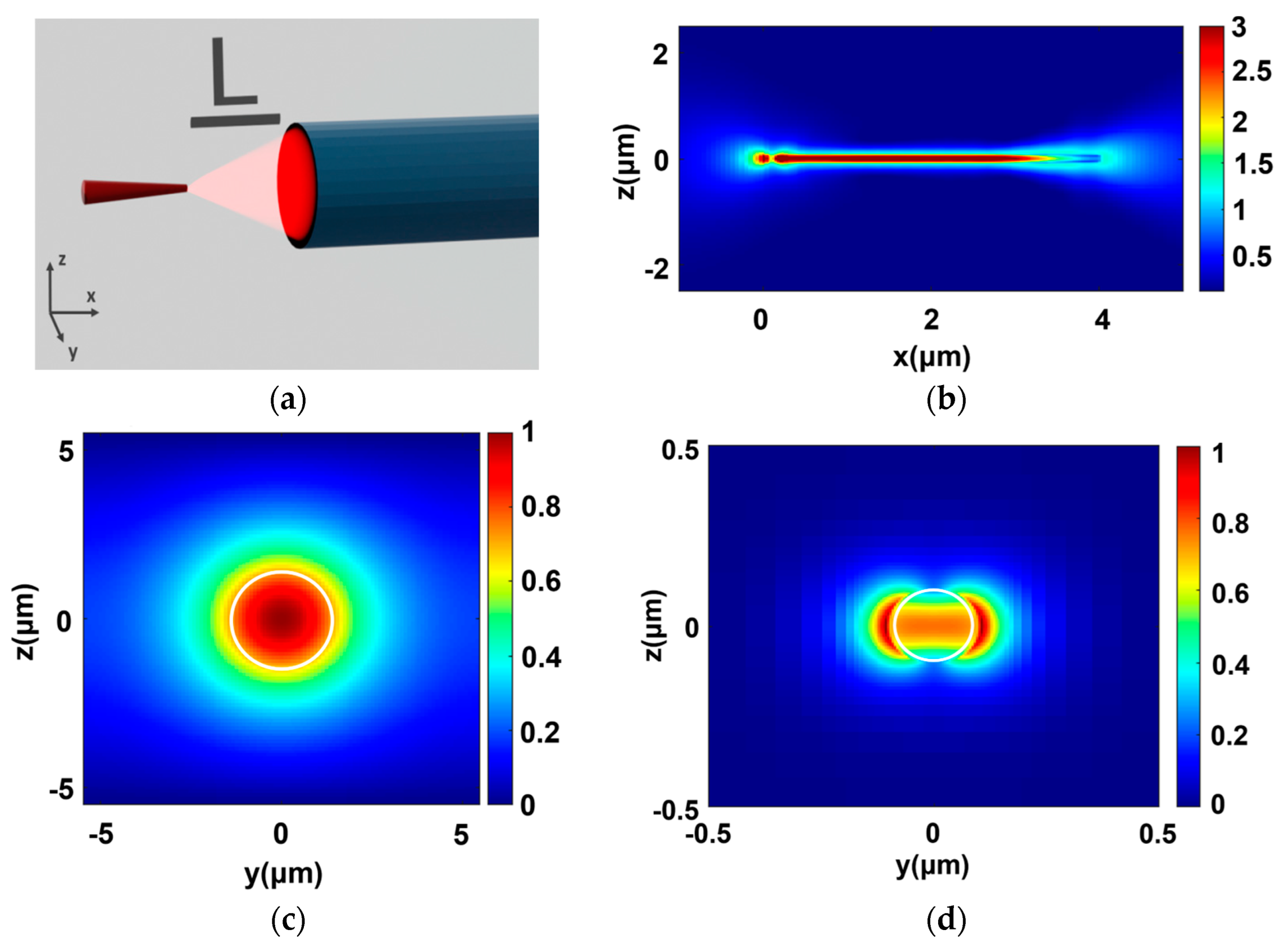
As an introduction to the aforementioned problem, an initial study on the coupling limitations is provided. As a physical-simulation scenario, it is considered an arrangement of a nanowire quantum-dot emitter and a buried channel waveguide in a homogeneous medium, as shown in
Figure 1a. The single-photon emitter is a typical [
39] III–V Indium Arsenide Phosphide InAsP QD, which is embodied in an Indium Phosphide InP NW during the growth process. The designed NW is 4 μm long with a diameter of 200 nm, while the taper diameter at the end of the NW is 109 nm, corresponding to a taper angle of 2°. The location of the QD is 200 nm from the NW’s base. This specific nanowire geometry is designed and tuned for 880 nm operating wavelength. The considered NWQD was a typical and characteristic option, with high availability for future experimental validation, while this choice does not restrict the applicability of the results in other nanowires of similar or larger dimensions, various tapering shapes, and at different operating wavelength bands, as also discussed in [
35].
We consider here the simplified case of a uniform cylindrical optical waveguide with a circular cross-section embedded in the homogeneous medium of a lower-refractive index. Such a channel waveguide refers to a typical laser written or, in general, a buried waveguide. To ensure single-mode operation for the photonic channel at the 880 nm QD’s emission wavelength, the refractive-index contrast, Δ = (n2core − n2cladding)/2n2core, between the core and the cladding has to be adjusted properly. For a silica medium (n = 1.452) as the cladding in our system, we assume a core-refractive index laser modification of Δn = 5·10−3 for a waveguide of 3 μm diameter. A refractive-index difference of this value ensures a single TE/TM mode operation and provides moderate confinement along the waveguide’s cross-section plane, thus striking a balance between light guidance and minimizing the effects of fabrication or modeling imperfections.
Initially, we examine the geometry shown in
Figure 1a, assuming that both NWQD and the WG are aligned in an inline arrangement and L is their relative distance. To facilitate our calculations, we regard that the whole structure (NWQD and WG) is surrounded by homogeneous SiO
2 material. In general, to achieve efficient coupling between the two distinct waveguides of different dimensions, one has to carefully design the two structures in order to obtain (i) similar effective refractive indices and (ii) maximum overlap integral between the fields of the two interacting modes. In our case, the supported TE/TM fundamental modes for both the NWQD and the SiO
2 waveguide are shown in
Figure 1c,d.
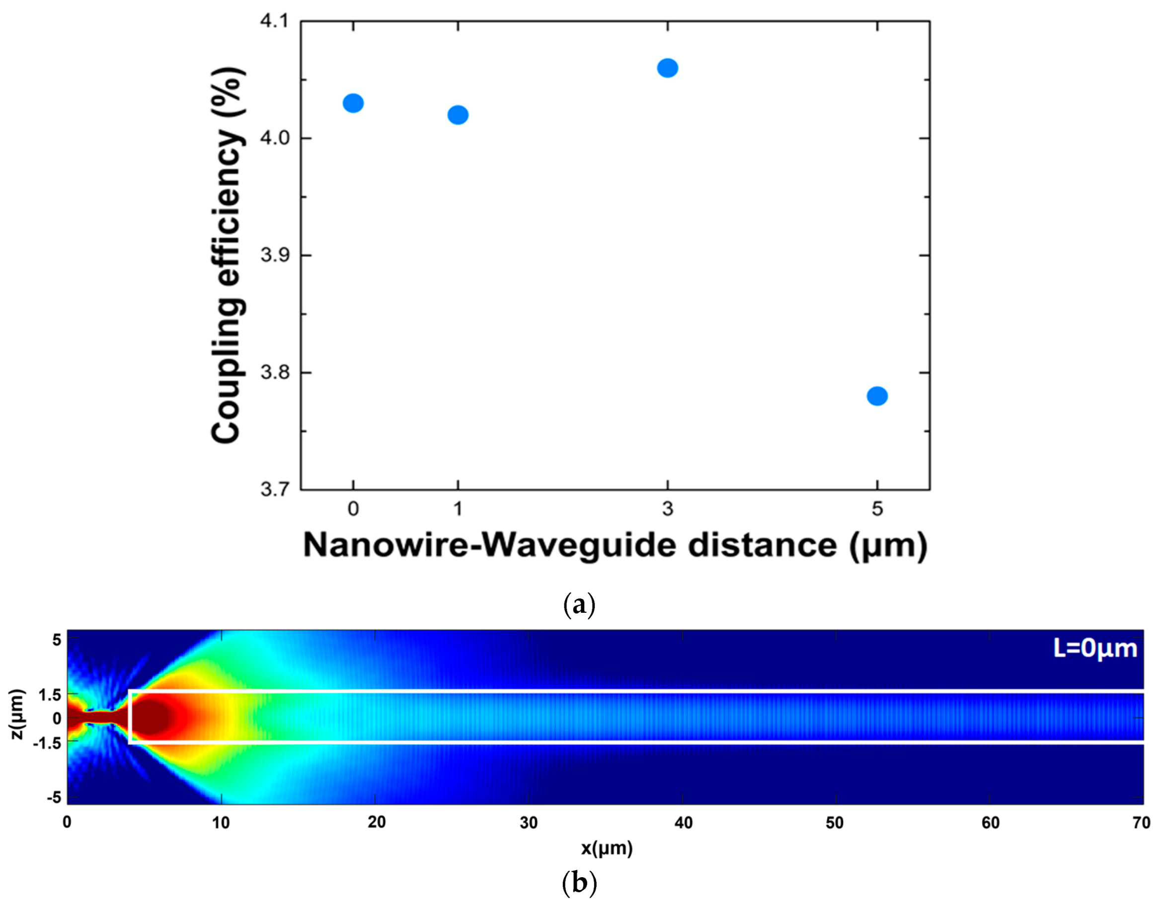
The calculation of the light coupling is performed by 3-dimensional (3D) Finite-Difference Time-Domain (FDTD) numerical simulations (Lumerical Inc, Vancouver, BC, Canada). The model considers the overlap between a QD TE electric dipole moment, embedded in the nanowire, and the waveguide’s fundamental TE mode to accurately compute the coupling. In
Figure 2a, the evaluated coupling values are shown as a function of the relative distance L for a TE dipole NWQD emission. The corresponding distribution of the TE electric field along the XZ plane is shown in
Figure 2b. From the electric field distribution at the XZ plane, we observe that most of the NWQD emitted light dissipates out of the waveguide, and only a small portion of that couples to the waveguide’s fundamental TE mode, dramatically reducing the coupling value to ~4%, while for higher coupling above 10%, a Δn much higher than 10
−2 is required [
35], which is beyond the current fabrication capabilities in silica platform. This finding confirms that the major hurdle behind the inefficient coupling between the NWQD and the WG is the large NA difference between the two photonic blocks due to the low-refractive index contrast of the channel waveguide.
3. NWQD–Waveguide Coupling Scheme
To overcome the aforementioned inherent light-coupling limitation and negate the high NA difference, the use of an optical dielectric microsphere as an intermediate element placed between the NWQD and the WG is proposed for the first time. It is demonstrated in the paper that in the mesoscale microsphere regime proposed here, the induced photonic nanojet [
40,
41,
42] succeeds in ejecting the light, illuminated by the NWQD, into the receiving channel waveguide.
Figure 3a illustrates the investigated photonic system with the addition of the microsphere represented in a generic case with a cylindrically shaped waveguide embedded in a uniform lower-refractive index medium. In the same
Figure 3a, a more realistic implementation of the microsphere’s arrangement between a buried channel waveguide and a suitably aligned nanowire is represented schematically. The incorporation of the nanowire and the microsphere in alignment with the waveguide would be possible with well-established micromachining techniques by the fabrication of suitable hosting slots by Reactive Ion Etching (RIE) or Focused Ion Beam (FIB) milling, which can have a resolution of better than 100 nm. This approach is also compatible with the fabrication approach of silica-based circuits with standard optical lithography for waveguide patterning, as it could also be used for the patterning of the nanowire and microsphere-hosting slots. In general, depending on the size of the microspheres and the required accuracy, lower-precision techniques such as femtosecond laser micromachining, followed by wet etching, could be used. Following the integration of nanowires and microspheres post-processing with a suitable polymer overlayer matched to silica-refractive index, which could seal and secure their placement. However, for clarity of the results’ presentation and the demonstration of the operating principle, we restrict our study here to the ideal case of a cylindrical waveguide, assuming a seamless integration of microsphere and nanowire. It has been confirmed by our studies that similar behavior and coupling performance can be achieved for the buried waveguide case. However, as this geometry includes various additional parameters for optimization, it will be reported in a future study.
More specifically, in this generic arrangement of the proposed coupling method, we consider that the separation between the end tip of NWQD and the adjacent surface of the microsphere is L, while the separation between the surface of the microsphere adjacent to the end of the waveguide and the waveguide is D. For a specified optical nanowire and a specified channel optical waveguide, the microsphere can be appropriately designed and selected in terms of characteristics, such as: (i) refractive index, (ii) dimension (diameter), and arranged properly in terms of (iii) geometrical separation between the nanowire and the microsphere, (iv) geometrical separation between the microsphere and the waveguide in order to achieve the maximum light coupling from the nanowire to the optical waveguide. In the generic case, the microsphere could be a proper dielectric microelement such as a cylinder, a half cylinder, or a half sphere. However, for simplicity, the study here was concentrated only on microspheres, which are readily available.
For a properly designed arrangement, the photonic nanojet emitted by the microsphere induces proper launching conditions near the adjacent waveguide, leading to proper excitation of the waveguide’s low-loss supported guided optical modes. It is stressed here that the proposed coupling system and method is based on this excitation of waveguides by the induced photonic nanojet. The microsphere does not act as a focusing ball lens that concentrates light into a single point, as it happens in other focusing techniques when using focusing balls of dimensions much greater than 30·λ, which is determined by geometrical optics principles with a well-defined optical focal point.
The microspheres considered in this study have a diameter in the range of 2–12 μm. In this scale, where the size of the microsphere is comparable to the wavelength of the incident light, their interaction with light cannot be described by a geometrical optics approach or by Rayleigh scattering formalism. However, a full description of light interaction with spherical particles of arbitrary size can be provided by the Mie theory and associated following formalisms as in [
42], where it has been shown that the field enhancement by dielectric mesoscale spheres (with radius R spanning from 1–30·λ) leads to a jet-shaped beam, usually called a photonic nanojet. The spatial characteristics of a photonic nanojet can be easily modulated [
40,
41,
42], as they depend on the microsphere size, the refractive index ratio between the microsphere, the surrounding material, and the wavelength of the light.
Until today, the employment of a microsphere for the generation of a photonic nanojet to launch and couple light in a waveguide was never considered and applied in practice, or, even more specifically, to launch light in a waveguide when illuminated by a nanowire or by a nanowire with a quantum dot acting as a single-photon source. Photonic nanojets were studied and demonstrated only in the following cases and applications: enhanced Raman spectroscopy, photolithography, nanoparticle detection and manipulation, enhanced optical absorption in photovoltaics and photodiodes, laser materials processing and dry laser cleaning, fluorescence sensing, and high-density optical data storage [
40], but not for coupling light to waveguides as described and demonstrated in this work.
3.1. Simulation of Photonic Nanojet Action
To highlight the role of the microsphere’s characteristics in the nanojet’s formation, such as the refractive index and radius, we initially simulate by FDTD a standalone microsphere illuminated by the NWQD, assuming no presence of a waveguide near the microsphere. Photonic nanojet simulation can be efficiently and reliably performed by the Finite Element Method (FEM) [
43] or by FDTD, as is used here, with an adequately dense computational grid [
41], leading to a very close agreement with analytical derivations based on the Bromwich scalar potential formulation [
42]. Here, an FDTD simulation approach was used to include and study light propagation in the entire system of the nanowire, microsphere, and channel waveguide. To formulate the problem, we consider microspheres with refractive index spanning from 1.6 to 2.5, simulating different microsphere materials such as polystyrene (n = 1.6), alumina (Al
2O
3, n
Al = 1.76), barium titanate (n
Ba = 1.9, 2.2) or titania (n
Ti = 2.5).
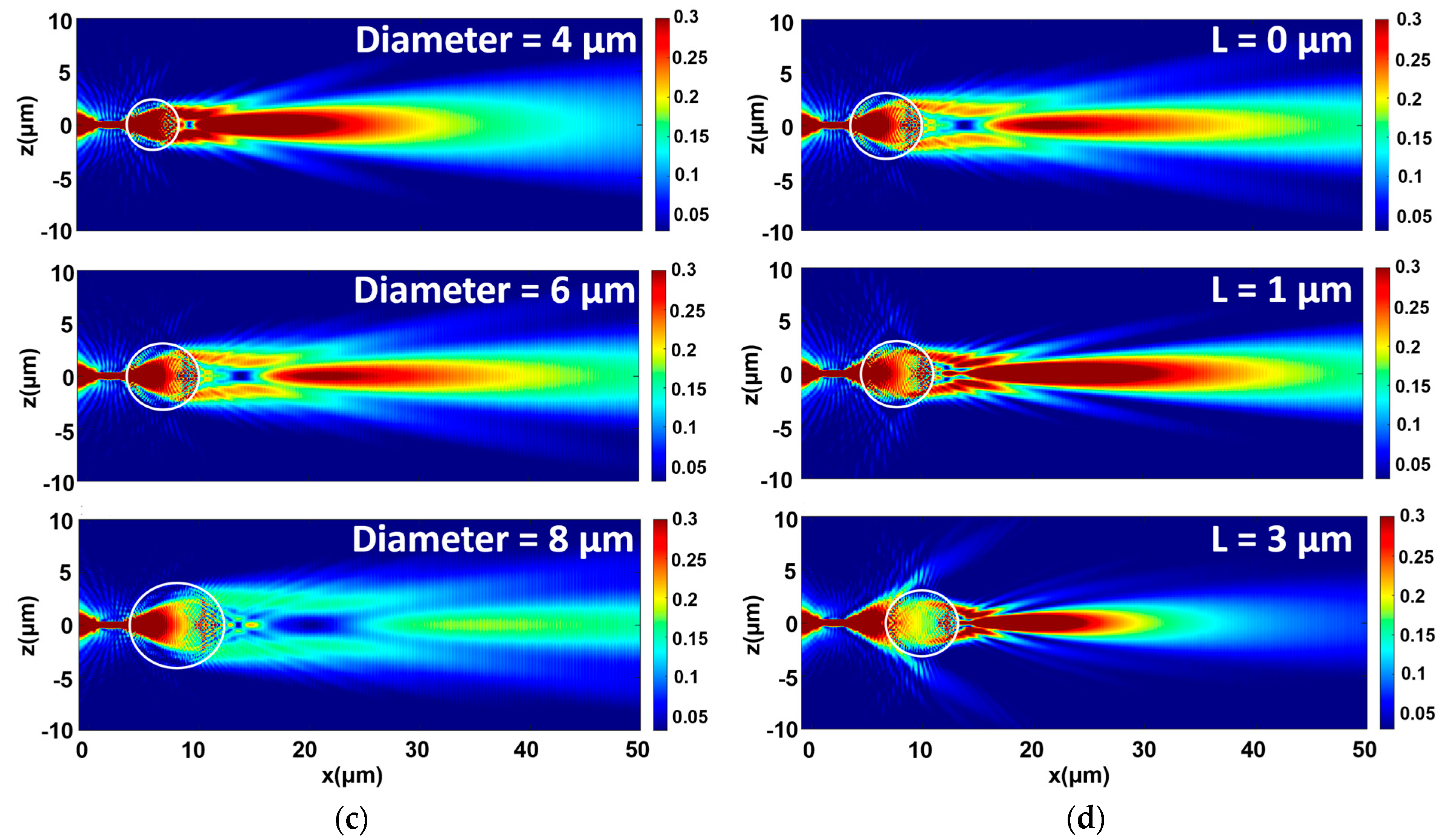
Figure 3b,c, summarizes the results obtained from FDTD simulations for different microsphere refractive indices and diameters at a NWQD–microsphere distance of L = 0 μm.
Figure 3d shows the nanojet formation for a NWQD–microsphere distance equal to L = 0, 1, 3 μm with a microsphere-refractive index of 1.9, and a diameter set to 6 μm. The background refractive index is n = 1.452.
In
Figure 3b, where the microsphere’s diameter is kept constant and equal to 6 μm, we observe that as the microsphere’s refractive index increases, the formation of the photonic nanojet occurs closer to the shadow side surface or even inside the microsphere for a high enough refractive index (e.g., 2.5). In addition, the nanojet’s elongation along the propagation axis reduces, the peak intensity increases, and the FWHM becomes narrower. The results presented here are in agreement with existing findings [
41]. In
Figure 3c, the effect of an increasing microsphere diameter with n = 1.9 is examined, and it is observed that the nanojet is formed effectively for lower-diameter microspheres. Additionally, in
Figure 3d, the distance between the nanowire and the microsphere is altered for the case of a microsphere with a diameter of 6 μm and a refractive index of 1.9. As the nanowire–microsphere distance increases from 0 μm to 1 μm and 3 μm, we notice that the nanojet increases in intensity with a shorter length along the propagation axis and moves closer to the microsphere’s shadow side. This observation is quite comprehensible, as in this specific microsphere with a relatively high refractive index (n = 1.9); when the distance from the source is increased, the microsphere collects the impinged light in a larger angle and redirects it closer to the shadow surface forming a more compact and higher-intensity photonic nanojet.
3.2. Coupling to Waveguide through the Nanojet Excitation
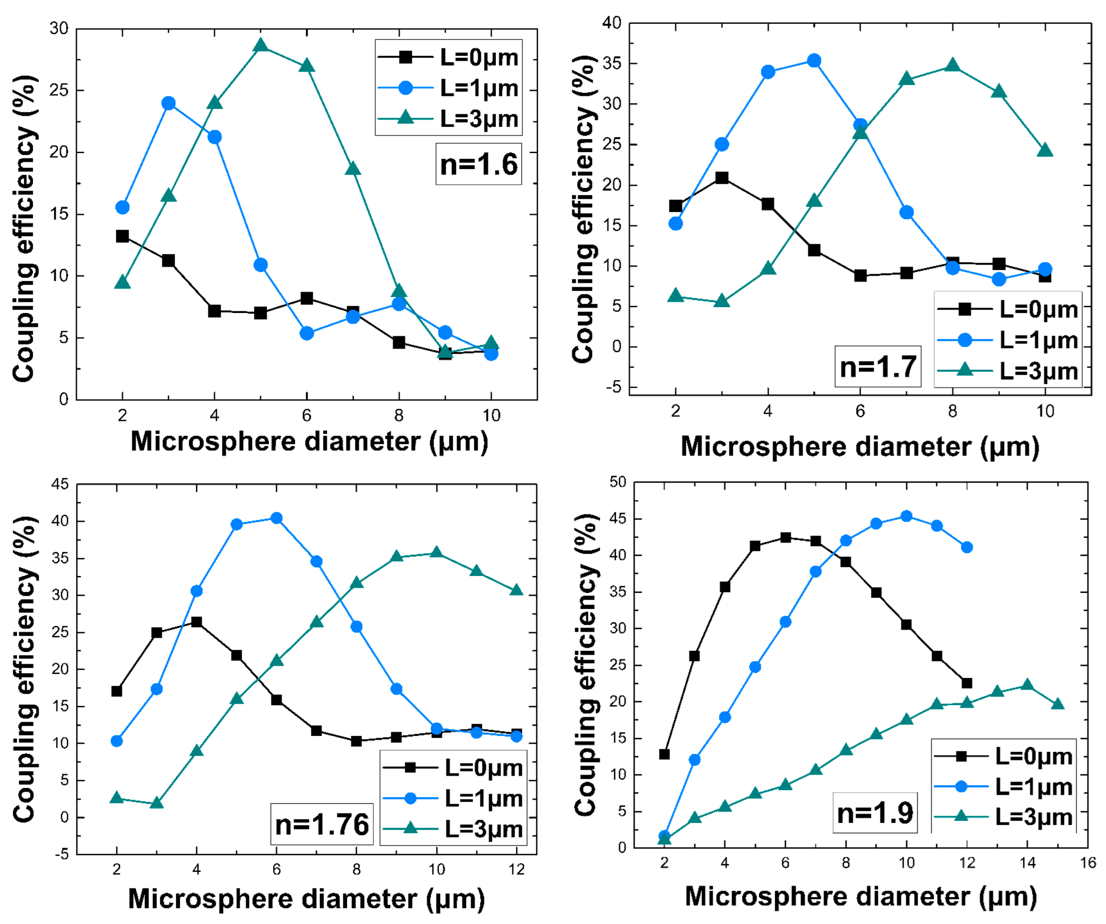
Το evaluate the effect of the microsphere in the NWQD–WG coupling, we conducted extensive 3D–FDTD simulations in the full photonic structure, as depicted in
Figure 3a. The parameters examined are the microsphere’s diameter and refractive index. Furthermore, to relate our study to a more realistic experimental implementation of a photonic circuit, we consider the effect of the relative distance L between the NWQD and the microsphere on the coupling calculation.
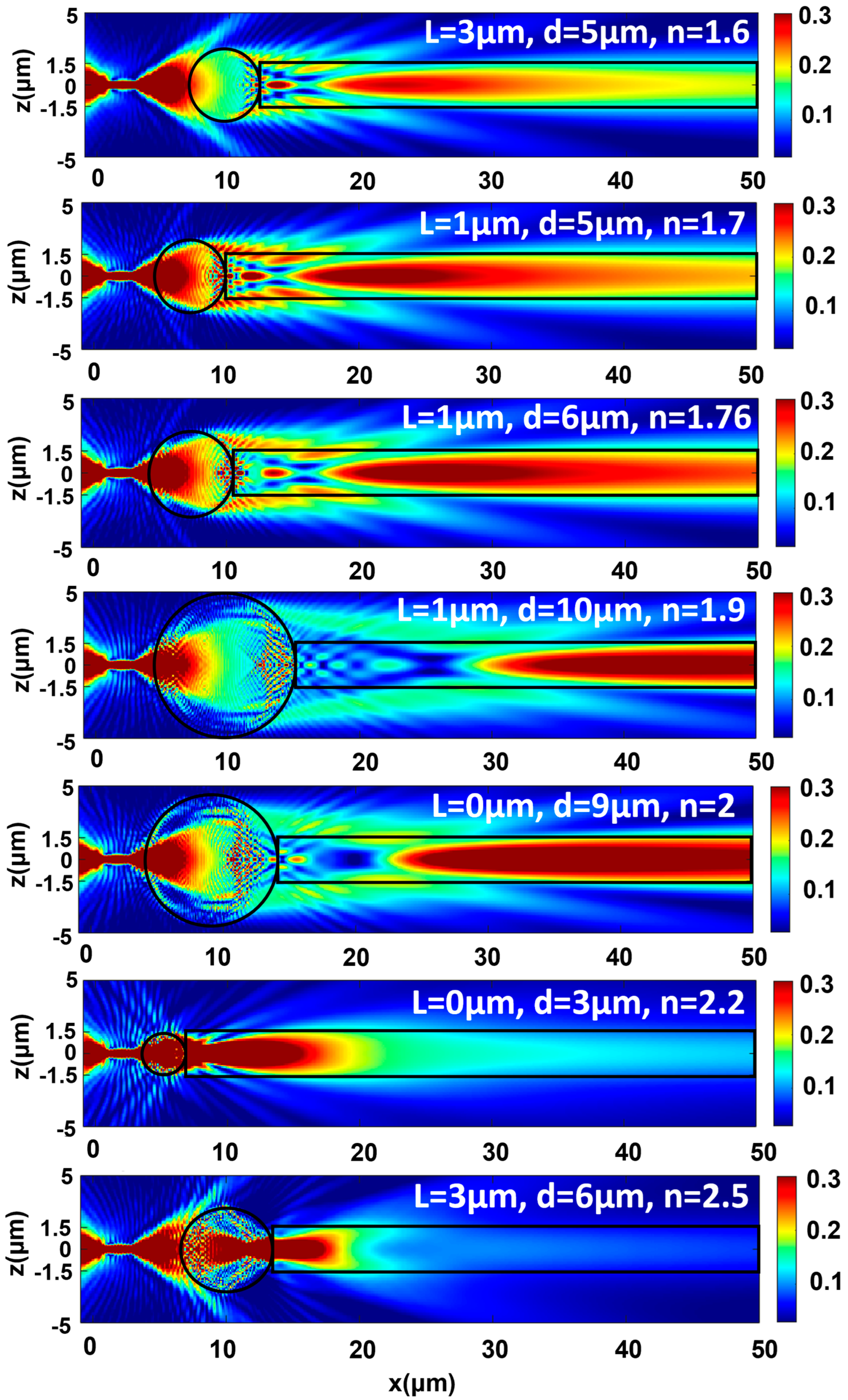
The coupling efficiency values are extracted for microspheres of different refractive index values (n = 1.6 to 2.5) and are plotted in
Figure 4 as a function of diameter and relative distance L. It is clearly demonstrated that the incorporation of a microsphere appears to significantly improve the NWQD–WG coupling by selecting the appropriate microsphere characteristics and the relative distance L. More specifically, TE mode coupling values as high as 40–45% can be achieved with a precise control of the relative distance L in the case of the n = 1.76, n = 1.9 and n = 2 microspheres, while for microspheres with a refractive index lower than 1.7 or higher than 2, the coupling is not efficient. Noteworthy is the fact that the coupling efficiency is very sensitive to the relative distance between the nanowire and the microsphere. Small deviations from the optimum design are possible to gradually downgrade the coupling efficiency. The coupling efficiency values extracted with the aid of a microsphere are more than an order of magnitude greater than those obtained without the microsphere by just butt-coupling the nanowire to the waveguide. The
Supplementary Material section provides visual details of the coupling mechanism for indicative cases of coupling for the configurations illustrated in
Figure 4. Coupling is demonstrated in
Figures S1a–S7a for the selected distance L that achieves a maximum coupling value for a specific diameter, while
Figures S1b–S7b provide a detailed view for the maximum coupling case.
To provide an intuitive view of the coupling mechanism,
Figure 5 presents a selection of the cases considered in
Figure 4 with the parameters selected for providing the highest coupling for each type of microsphere. Depending on the considered parameters, it is shown how the nanojets are injected in the adjacent waveguide, transferring their energy to the supported fundamental guided mode of the channel waveguide. In
Figure 4, it is clear for a few cases of strong coupling for n = 1.7, 1.76, and 1.9, the existence of two distinct peaks with comparable maximum coupling corresponding to different L. As can be observed from
Figure 3c,d, the interplay between diameter and distance L can provide conditions for comparable efficient coupling, but in different ways by directing the light in different positions along the waveguide, as clearly seen also in
Figure 5. For clarity, the different ways of coupling are demonstrated comparatively in the
Supplementary Material section in Figure S3b,c and Figure S4b,c for microspheres with a refractive index of n = 1.76 and 1.9, respectively.
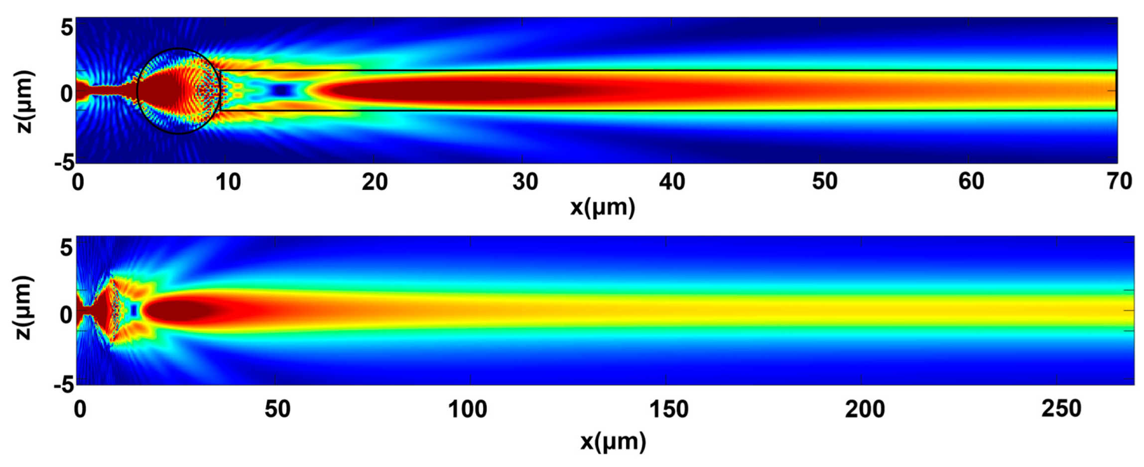
In order to demonstrate clearly the reliable steady state condition of coupling the nanojets’ light into the waveguide’s supported modes, the coupling mechanism for the representative case of a highly efficient coupling through a 6 μm diameter, n = 1.9 microsphere at L = 0 μm and over 70 μm and 250 μm of waveguide propagation, is presented in
Figure 6. In the case of 70 μm of propagation, the details of the nanojet formation in the presence of the waveguide can be seen, while in 250 μm of propagation, the smooth steady-state propagation of the supported mode is presented.
4. Design Tolerances in the Coupling Scheme
Additionally, other secondary parameters also affect the coupling efficiency in the proposed method and are considered for the theoretical determination of the optimum coupling. These parameters determine the tolerances of the design and are: (i) the effect of distance D between the microsphere and the waveguide, (ii) the angle of the NWQD axis to the central axis of the microsphere that is aligned to the axis of the waveguide, inducing a misalignment, (iii) the degree of sphericity of the microsphere, (iv) the lateral (Y- or Z-direction) displacement of the NWQD, and (v) the design operating wavelength. It should be noted that even though the distance D is a key parameter in the optimal arrangement of the proposed coupling scheme (as discussed above) due to the fact that it has a less drastic effect to the coupling performance, it was chosen to be considered and studied here, in the tolerances section, for clarity of presentation reasons.
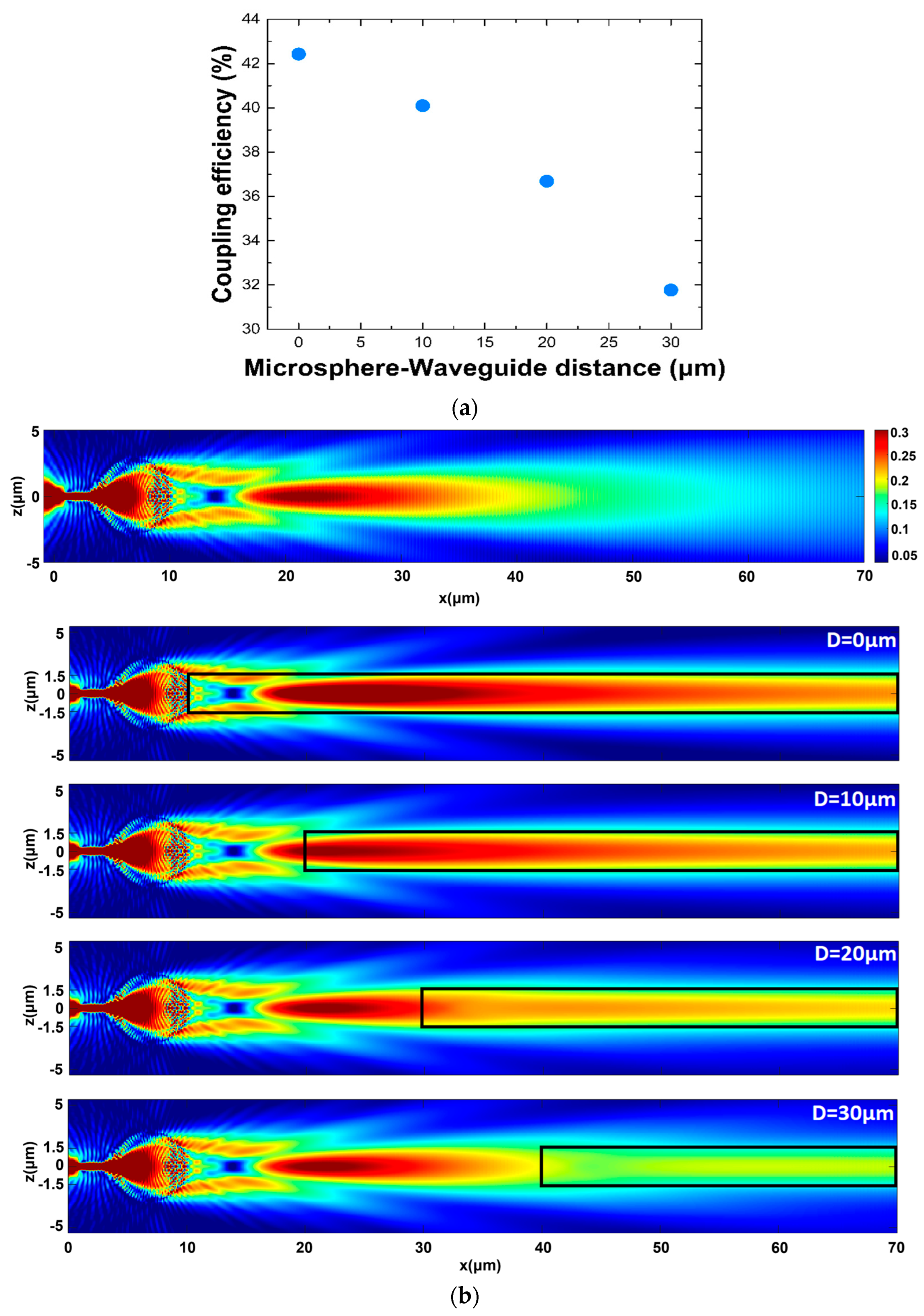
4.1. Effect of Microsphere—Waveguide Distance
Firstly, we examine the case where the microsphere and the waveguide are no longer in contact but are separated by a gap D, as shown earlier in
Figure 3a.
In this section, we consider a microsphere with a diameter of 6 μm and a refractive index of 1.9 with the distance L between the nanowire and the microsphere set to 0 μm, while the distance D between the microsphere and the waveguide is increased from 0 μm to 10 μm, 20 μm, and 30 μm. The corresponding coupling efficiency values versus the gap distance D is shown in
Figure 7a.
Figure 7b presents from top to down the generated photonic nanojets, starting with the first nanojet by neglecting the presence of the waveguide, and followed by the electric-field distribution along the propagation axis as the waveguide is moved further away from the microsphere, from 0 to 30 μm. While obtaining a coupling value over 42% when the microsphere and the waveguide are in contact when their separation increases by 10 μm, the coupling efficiency appears to drop down only by 2%. By further increasing this gap, the coupling efficiency value keeps decreasing, achieving a value of 37% for a 20 μm gap and about 32% for a 30 μm gap. Comparing the electric-field distributions to the case where the nanojet is formed in the medium with no waveguide present, we observe the additional confinement of the nanojets inside the waveguide boundaries forcing the excitation of the guided modes.
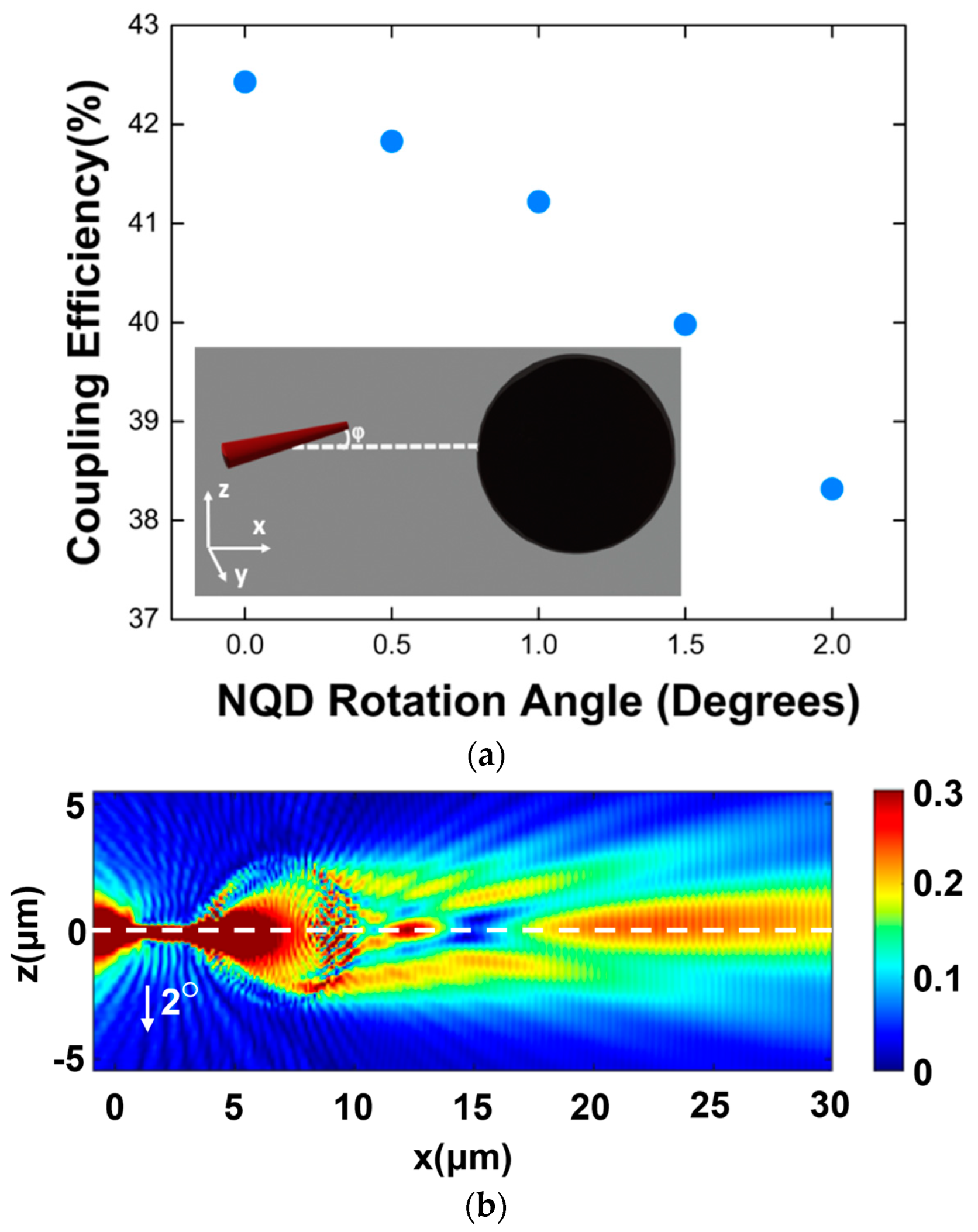
4.2. Effect of NWQD Tilt Angle
The accurate placement of the NWQD and its alignment with the rest of the photonic blocks is typically performed by accurate “pick and place” transfer techniques, e.g., by employing micro/nano manipulators [
29,
30].
However, the effect of any tilt misalignments due to an induced tilt of angle φ related to the central axis of a microsphere is also considered. To get a better view on the aforementioned misalignment effect on the coupling efficiency, we performed numerical simulations, rotating the NWQD with an angle φ in respect to the nominal propagation axis, as shown in
Figure 8.
In
Figure 8b, the NWQD–WG coupling is presented, varying the angle to 2°. To carry out these simulations, an arrangement with L = 0 μm and with a microsphere with a 6 μm radius and refractive index n = 1.9 was considered. Despite the rotating angle misalignment between the NWQD and the microsphere, the coupling remains high, reduced only by 4% for a maximum rotation angle of 2°, exhibiting the robustness of the system under experimental misalignment issues. State-of-the-art micromanipulation techniques can provide a very accurate control of positioning eliminating tilts to angles below 1 degree. Therefore, the proposed method is relatively robust to such tilts.
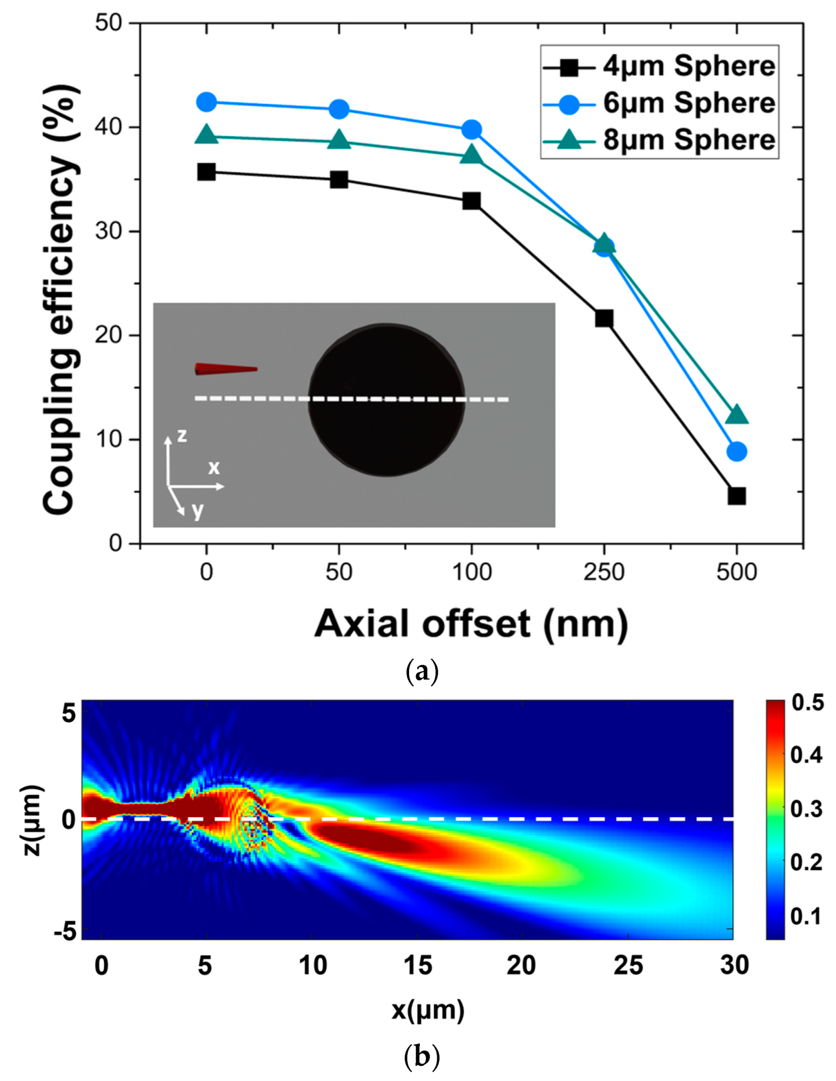
4.3. Effect of NWQD Lateral Displacement
Similarly, the effect of the NWQD lateral displacement is examined. In contrast to the NWQD tilt scenario, here, the NWQD is completely off-axis without inducing any angle, as depicted in
Figure 9a (inset image). Therefore, if the emitted light cone is laterally misplaced, it will result in the point of intersection with the microsphere’s surface occurring a few nanometers away from its center.
This will lead the photonic nanojet to be formed with no axial symmetry related to the microsphere’s waveguide axis, pointing now with an angle depending on the axis’ misalignment of the NWQD, as shown in
Figure 9. In
Figure 9a, the coupling efficiency values are extracted for an NWQD-Microsphere-Waveguide arrangement where the NWQD is laterally displaced in the Z-axis (or in the equivalent Y-axis) by 50, 100, 250, and 500 nanometers for 4, 6, and 8 μm-diameter microspheres. It is evident that for an offset up to 100 nm, the coupling efficiency for all cases is decreased by just ~2%. By moving the NWQD further away, though, the coupling efficiency starts to decrease at a higher rate, leading to an output value of ~10% at 500 nm off. Also, as expected, the larger 8 μm microsphere appears to be more tolerant since the displacement for smaller spheres will shift the NWQD emission even further from the center of the microsphere.
4.4. Effect of Sphericity Ratio
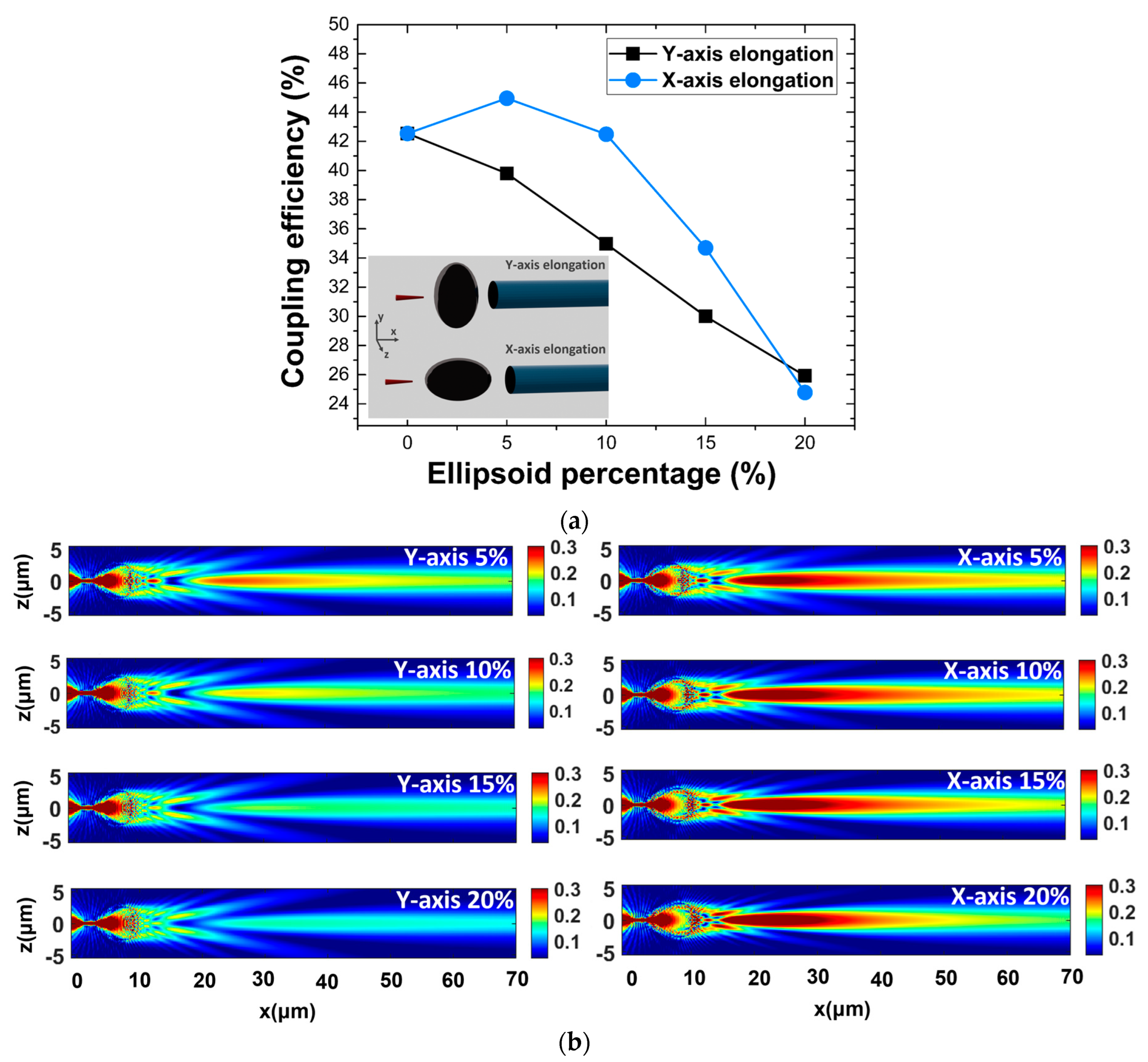
The efficiency of the proposed coupling scheme is also examined in terms of the microsphere shape. Chemically produced microspheres, typically, have a high sphericity ratio approaching the perfect spherical shape. However, there is a small percentage of microparticles that are not perfect spheres; rather, they have a more elliptical shape.
FDTD simulations were performed for the case of a microsphere (n = 1.9, 6 μm diameter) between the NWQD and the waveguide, which is elongated along either the Y-axis (or, equivalently, the Z-axis due to symmetry) or the X-axis, while the light propagation is monitored in the X-axis. The ellipticity
e of the microsphere (or ellipsoid percentage) is defined here as
e = (a − b)/b, where a and b are the sphere radii in Y(Z) and X main axes. It is shown that the effect of the ellipsoidal microsphere medium results in a linear decrease of the coupling efficiency as the sphere deformation and ellipticity increases. The coupling efficiency values are presented in
Figure 10a for both the X-axis and Y-axis, and in
Figure 10b, the electric-field distribution along the X propagation axis is presented for a number of ellipsoids prolonged along both axes at a percentage of up to 20%. We observed an anomalous behavior for the Y elongation case for a small deformation of 5%, with an increased coupling that could be attributed to the specific more efficient collection of NWQD light by the microsphere’s increased illuminated surface.
4.5. Effect of Operating Wavelength
Finally, in the showcased results, we considered an NWQD emitter centered at 880 nm. However, in practical PICs, one or more single-photon sources can be incorporated emitting at more than one wavelength. Therefore, the robustness of the proposed configuration needs to be examined for different emission wavelengths other than the optimal designed one. The requirement is that a specific microsphere can couple light from different NWQDs emitted at different adjacent wavelengths, easing the hybrid circuit fabrication by using only one type and size of microsphere at different/multiple input ports. Furthermore, new developments in NWQDs have enabled the integration of multiple QDs in a single nanowire [
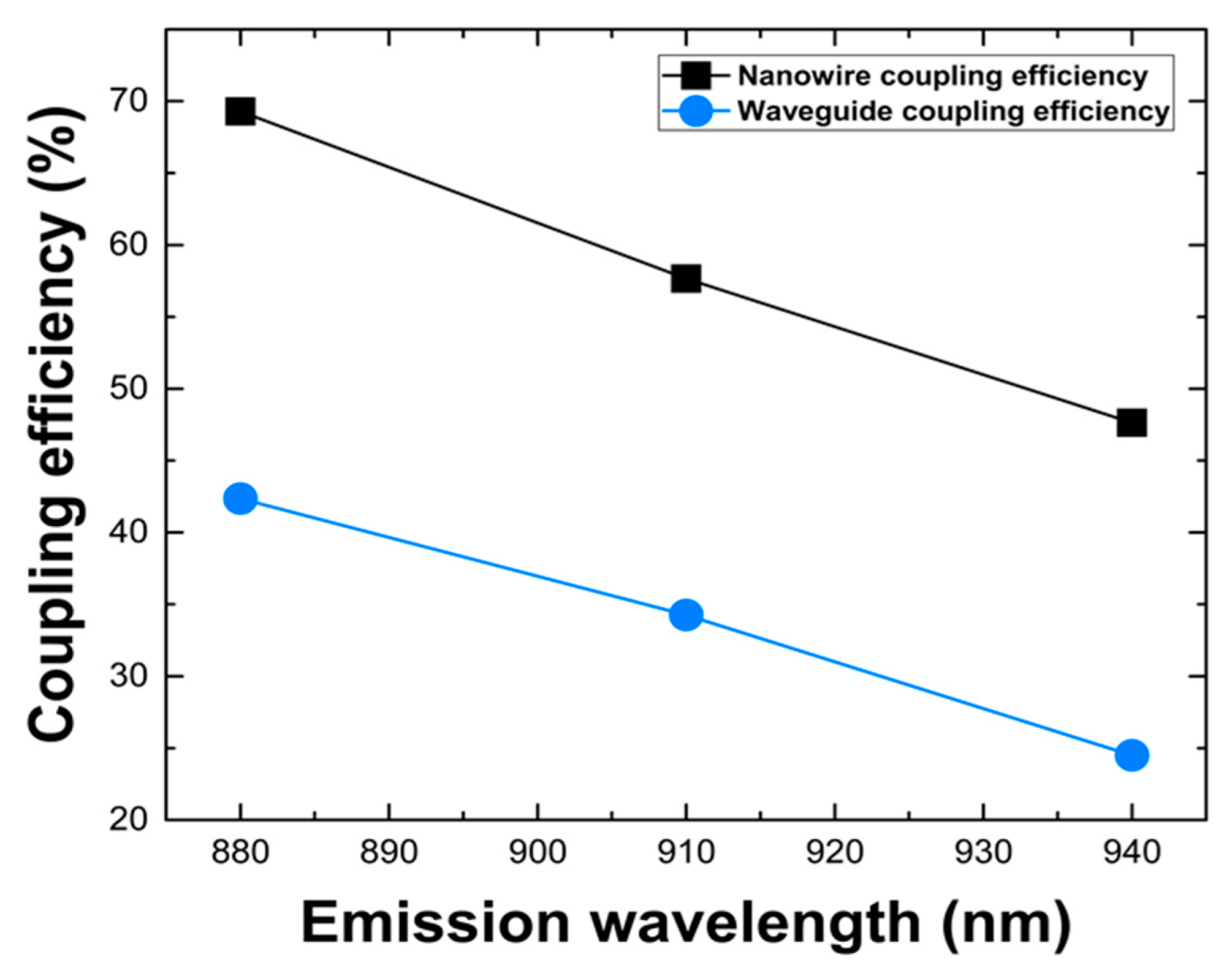
44], and, therefore, a single-optimized microsphere should ideally couple light efficiently at the multiple wavelengths corresponding to multiple QDs in a nanowire. With the considered nanowire, we examine its operation with three different QDs operating and emitting at 880 nm, 910 nm, and 940 nm wavelengths. The QD emission was simulated by a dipole moment incorporated in the nanowire.
As can be seen in
Figure 11 the dipole emission exhibits a coupling efficiency to the specific nanowire waveguide of ~70% for a wavelength of 880 nm, dropping to ~60% for 910 nm, and to ~50% for 940 nm wavelengths. In
Figure 11, we present the total coupling performance from nanowire to the waveguide by considering a coupling scheme with a 6 μm diameter microsphere of n = 1.9. Inspecting this decreasing trend in both coupling curves in
Figure 11, as the wavelength increases, it indicates that the lower overall coupling values in the longer wavelengths are due to the initial coupling of the QD to the nanowire’s waveguide structure for increased wavelength values, denoting that the coupling through the microsphere is not greatly affected by different wavelengths. Therefore, a hybrid circuit with an embedded specific microsphere can be operable for a range of wavelengths without complicating the structure while also allowing for nanowires with multiple quantum dots. The simultaneous action of multi dots in a nanowire, coupled through a single microsphere, could enable an efficient multiwavelength operation in such hybrid circuits.
5. Discussion and Conclusions
This paper deals with current challenges in the integration of single photon sources in optical waveguides for the development of hybrid quantum optical circuits and devices for quantum manipulation and processing of single photons towards quantum computing, communication, and sensing applications. One major category of single-photon sources is based on quantum dots that are embedded in semiconductor optical nanowires (NWQD). A recently published study [
35] identified in a systematic way the serious limitations for coupling NWQD in low-refractive index contrast channel waveguides, which are usually fabricated in the silica-based platform by lithography or by direct laser writing, or also generally by in-diffusion processes in various material platforms, thus limiting the coupling efficiency to <5%, which is impractical for quantum applications.
This study proposed, for the first time, a method for the efficient light coupling of semiconductor nanowires to optical waveguides by the insertion between them of a dielectric microsphere suitably designed in terms of: (1) size of the microsphere, (2) refractive index of microsphere, (3) distance between the nanowire and the microsphere, (4) distance between microsphere and waveguide. Such an optimal arrangement assures the generation of a photonic nanojet from the illuminated microsphere with suitable spatial and optical characteristics that enable the efficient excitation of the waveguide’s eigenmodes and, finally, the light coupling to the channel waveguide through the microsphere.
The proposed method is demonstrated in the case of a typical InP nanowire with an embedded InAsP quantum dot, emitting at 880 nm with a length of 4 μm and a diameter of 200 nm. The considered waveguide simulated a silica-based cylindrical waveguide with 3μm of diameter and a refractive index step of 5·10−3 compared to pure silica, which was attributed to a typical laser-induced refractive index change. It was demonstrated that by using readily available microspheres of barium titanate (n = 1.9) or alumina (n = 1.76), with diameters around 5 μm, a coupling > 45% could be achieved, while for laser-written waveguides with a refractive index step > 5·10−3, the coupling could easily exceed 50%. By properly incorporating Bragg gratings as reflectors to the back propagating emission from the nanowire, this coupling could be enhanced even further. As demonstrated, the proposed theoretical design exhibits adequate tolerances in terms of distance between the microsphere and nanowire, or waveguide, the sphericity of the microsphere, the tilt misalignment, the lateral displacement, and the operating wavelength. It should be noted that even in the case of microspheres’ manual assembly, which is intrinsically compatible with the nanowires’ transfer by the “pick and place“ technique; the design requirements can be met as the micromanipulators for nanowire and microsphere placement exhibit typical accuracy better than 20 nm distance and a 1-degree tilt angle. Furthermore, the accuracy of hosting micro-patterned slots for the nanowire and microsphere can be better than 100 nm by following RIE or FIB techniques. Therefore, the standardization of the process could provide a robust and viable solution.
New advances in the development of 3D printing of microlenses by multiphoton laser lithography [
45] could provide useful tools for the monolithic integration of microspheres and a facilitation of nanowire coupling. Furthermore, new photonic assembly techniques based on 3D-printed facet-attached microlenses [
46] in optical circuits could be also investigated in terms of their adaptability to host nanowires in a controllable way as quantum emitters. However, it is anticipated that the requirement of high-refractive index (>1.75) microspheres would be very challenging to be met by the 3D printing of mainly polymer materials. Additionally, the integration of nanowires would require further customizability, such as, for example, accurate placement in specific areas of the circuit combined with adjacent Bragg Gratings to direct forward the back-propagated radiation of nanowires. Such optimization steps would be difficult to implement in the facet-attached micro-lens platforms. The microsphere-based coupling scheme could be also investigated and applied to optical fibers or fiber arrays. However, the fabrication methodology and tolerances of typical fiber arrays (V-groove assemblies) will need to be carefully considered.
Our findings offer new opportunities towards the realization of silica-based hybrid-integrated photonic circuits by on-chip integration of multiple nanowire single-photon emitters with applications in various fabrication platforms and, especially, in the most challenging case of directly laser-written waveguides of low-refractive index contrast in silica and silica-on-silicon platforms.
The current study seeks to demonstrate the successful coupling of NWQD to low-confinement waveguides through realizable approaches in specific cases while, due to the complication of the study, cannot provide, at this stage, generic engineering rules for designing and selecting the appropriate microspheres, although this theoretical study based on an analytical formulation, as in [
42], could be triggered by this work. Further work of the fabrication tolerances and integration approaches in specific silica-on-silicon platforms is under consideration and will be reported in a future study.
It is strongly anticipated that the proposed coupling scheme, which solves a challenging problem, will enable the facilitation of silica-based optical circuits towards the development of highly customizable and scalable quantum photonic-integrated circuits, which are crucial for quantum-computing applications.
6. Patents
C. Riziotis: “Light coupling between nanowire and optical waveguide by microsphere photonic nanojet,” European Patent Office, Patent Application Number EP23386114.5 (Filing date 09-11-2023).
Supplementary Materials
The following supporting information can be downloaded at:
https://www.mdpi.com/article/10.3390/photonics11040343/s1. Figure S1: Coupling for a microsphere with n = 1.6; Figure S2: Coupling for a microsphere with n = 1.7; Figure S3: Coupling for a microsphere with n = 1.76; Figure S4: Coupling for a microsphere with n = 1.9; Figure S5: Coupling for a microsphere with n = 2.0; Figure S6: Coupling for a microsphere with n = 2.2; Figure S7: Coupling for a microsphere with n = 2.5. The supplementary material section provides details of the coupling mechanism for the coupling arrangement configurations presented in
Section 3.2 of the manuscript, for microspheres of refractive indices, with values n = 1.6, 1.7, 1.76, 1.9, 2.0, 2.2, and 2.5, and with various diameters. For each individual graph in
Figure 4 of the paper, corresponding to a specific refractive index, Figures S1–S7 present visually the coupling mechanism by the photonic nanojet’s excitation, for various examined microspheres’ diameters, and for a specific distance L, which corresponds to the maximum observed coupling value. Each one of Figures S1a–S7a presents the light propagation along distance of 120 μm, as well as a magnified version of the graphs of
Figure 5 in Figures S1b–S7b for a greater propagation distance of 70 μm. Figures S3c and S4c provide, additionally, two indicative suboptimum coupling cases for comparison with the corresponding optimum cases.
Author Contributions
Conceptualization: C.R.; Methodology, C.R.; Validation, C.R., S.I.T., K.T., J.C.G., A.W.E., V.Z. and P.G.R.S.; Formal Analysis, C.R., S.I.T. and K.T.; Investigation, C.R., S.I.T., K.T., J.C.G., A.W.E., V.Z., P.G.R.S. and C.R.; Writing—Original Draft Preparation, C.R., S.I.T. and K.T.; Writing—Review and Editing, C.R., S.I.T., K.T., J.C.G., A.W.E., V.Z. and P.G.R.S.; Visualization, S.I.T. and K.T.; Supervision, C.R.; Project Administration, C.R.; Funding Acquisition, C.R. All authors have read and agreed to the published version of the manuscript.
Funding
This research work was supported by the Hellenic Foundation for Research and Innovation (H.F.R.I.) under the “First Call for H.F.R.I. Research Projects to support Faculty members and Researchers and the procurement of high-cost research equipment grant” (Project Number: HFRI-FM17-640, InPhoQuC).
Institutional Review Board Statement
Not applicable.
Informed Consent Statement
Not applicable.
Data Availability Statement
No new data were created in this study. Data sharing is not applicable to this article.
Conflicts of Interest
The authors declare no conflict of interest.
References
- Wang, J.; Sciarrino, F.; Laing, A.; Thompson, M.G. Integrated photonic quantum technologies. Nat. Photon. 2019, 14, 273–284. [Google Scholar] [CrossRef]
- Politi, A.; Cryan, M.J.; Rarity, J.G.; Yu, S.; O’Brien, J.L. Silica-on-silicon waveguide quantum circuits. Science 2008, 320, 646–649. [Google Scholar] [CrossRef] [PubMed]
- Matthews, J.C.; Politi, A.; Stefanov, A.; O’Brien, J.L. Manipulation of multiphoton entanglement in waveguide quantum circuits. Nat. Photonics 2009, 3, 346–350. [Google Scholar] [CrossRef]
- Shadbolt, P.J.; Verde, M.R.; Peruzzo, A.; Politi, A.; Laing, A.; Lobino, M.; Matthews, J.C.; Thompson, M.G.; O’Brien, J.L. Generating, manipulating and measuring entanglement and mixture with a reconfigurable photonic circuit. Nat. Photonics 2011, 6, 45–49. [Google Scholar] [CrossRef]
- Laing, A.; Peruzzo, A.; Politi, A.; Verde, M.R.; Halder, M.; Ralph, T.C.; Thompson, M.G.; O’Brien, J.L. High-fidelity operation of quantum photonic circuits. Appl. Phys. Lett. 2010, 97, 211109. [Google Scholar] [CrossRef]
- Smith, B.J.; Kundys, D.; Thomas-Peter, N.; Smith, P.G.R.; Walmsley, I.A. Phase-controlled integrated photonic quantum circuits. Opt. Express 2009, 17, 13516–13525. [Google Scholar] [CrossRef]
- Corrielli, G.; Crespi, A.; Geremia, R.; Ramponi, R.; Sansoni, L.; Santinelli, A.; Mataloni, P.; Sciarrino, F.; Osellame, R. Rotated waveplates in integrated waveguide optics. Nat. Commun. 2014, 5, 4249. [Google Scholar] [CrossRef]
- Sansoni, L.; Sciarrino, F.; Vallone, G.; Mataloni, P.; Crespi, A.; Ramponi, R.; Osellame, R. Polarization entangled state measurement on a chip. Phys. Rev. Lett. 2010, 105, 200503. [Google Scholar] [CrossRef]
- Crespi, A.; Ramponi, R.; Osellame, R.; Sansoni, L.; Bongioanni, I.; Sciarrino, F.; Vallone, G.; Mataloni, P. Integrated photonic quantum gates for polarization qubits. Nat. Commun. 2011, 2, 566. [Google Scholar] [CrossRef]
- Aspuru-Guzik, A.; Walther, P. Photonic quantum simulators. Nat. Phys. 2012, 8, 285–291. [Google Scholar] [CrossRef]
- Arrazola, J.M.; Bromley, T.R.; Izaac, J.; Myers, C.R.; Brádler, K.; Killoran, N. Machine learning method for state preparation and gate synthesis on photonic quantum computers. Quantum Sci. Technol. 2019, 4, 024004. [Google Scholar] [CrossRef]
- Carolan, J.; Mohseni, M.; Olson, J.P.; Prabhu, M.; Chen, C.; Bunandar, D.; Niu, M.Y.; Harris, N.C.; Wong, F.N.; Hochberg, M.; et al. Variational quantum unsampling on a quantum photonic processor. Nat. Phys. 2020, 16, 322–327. [Google Scholar] [CrossRef]
- Steinbrecher, G.R.; Olson, J.P.; Englund, D.; Carolan, J. Quantum Optical Neural Networks. npj Quantum Inf. 2019, 5, 60. [Google Scholar] [CrossRef]
- Somaschi, N.; Giesz, V.; De Santis, L.; Loredo, J.C.; Almeida, M.P.; Hornecker, G.; Portalupi, S.L.; Grange, T.; Antón, C.; Demory, J.; et al. Near-optimal single-photon sources in the solid state. Nat. Photonics 2016, 10, 340–345. [Google Scholar] [CrossRef]
- Ding, X.; He, Y.; Duan, Z.-C.; Gregersen, N.; Chen, M.-C.; Unsleber, S.; Maier, S.; Schneider, C.; Kamp, M.; Höfling, S.; et al. On-demand single photons with high extraction efficiency and near-unity indistinguishability from a resonantly driven quantum dot in a micropillar. Phys. Rev. Lett. 2016, 116, 020401. [Google Scholar] [CrossRef] [PubMed]
- Sipahigil, A.; Jahnke, K.D.; Rogers, L.J.; Teraji, T.; Isoya, J.; Zibrov, A.S.; Jelezko, F.; Lukin, M.D. Indistinguishable photons from separated silicon-vacancy centers in Diamond. Phys. Rev. Lett. 2014, 113, 113602. [Google Scholar] [CrossRef] [PubMed]
- Bogdanov, S.; Shalaginov, M.Y.; Boltasseva, A.; Shalaev, V.M. Material platforms for integrated quantum photonics. Opt. Mater. Express 2016, 7, 111–132. [Google Scholar] [CrossRef]
- Mennea, P.L.; Clements, W.R.; Smith, D.H.; Gates, J.C.; Metcalf, B.J.; Bannerman, R.H.; Burgwal, R.; Renema, J.J.; Kolthammer, W.S.; Walmsley, I.A.; et al. Modular linear optical circuits. Optica 2018, 5, 1087–1090. [Google Scholar] [CrossRef]
- Zhang, Q.; Li, M.; Chen, Y.; Ren, X.; Osellame, R.; Gong, Q.; Li, Y. Femtosecond laser direct writing of an integrated path-encoded CNOT quantum gate. Opt. Mater. Express 2019, 9, 2318–2326. [Google Scholar] [CrossRef]
- Atzeni, S.; Rab, A.S.; Corrielli, G.; Polino, E.; Valeri, M.; Mataloni, P.; Spagnolo, N.; Crespi, A.; Sciarrino, F.; Osellame, R. Integrated sources of entangled photons at the telecom wavelength in femtosecond-laser-written circuits. Optica 2018, 5, 311–314. [Google Scholar] [CrossRef]
- Senellart, P.; Solomon, G.; White, A. High-performance semiconductor quantum-dot single-photon sources. Nat. Nanotechnol. 2017, 12, 1026–1039. [Google Scholar] [CrossRef] [PubMed]
- Arakawa, Y.; Holmes, M.J. Progress in quantum-dot single photon sources for quantum information technologies: A broad spectrum overview. Appl. Phys. Rev. 2020, 7, 021309. [Google Scholar] [CrossRef]
- Lu, C.-Y.; Pan, J.-W. Quantum-dot single-photon sources for the quantum internet. Nat. Nanotechnol. 2021, 16, 1294–1296. [Google Scholar] [CrossRef] [PubMed]
- Claudon, J.; Bleuse, J.; Malik, N.S.; Bazin, M.; Jaffrennou, P.; Gregersen, N.; Sauvan, C.; Lalanne, P.; Gérard, J.-M. A highly efficient single-photon source based on a quantum dot in a photonic nanowire. Nat. Photonics 2010, 4, 174–177. [Google Scholar] [CrossRef]
- Mäntynen, H.; Anttu, N.; Sun, Z.; Lipsanen, H. Single-photon sources with quantum dots in III–V nanowires. Nanophotonics 2019, 8, 747–769. [Google Scholar] [CrossRef]
- Chang, J.; Gao, J.; Esmaeil Zadeh, I.; Elshaari, A.W.; Zwiller, V. Nanowire-based integrated photonics for quantum information and quantum sensing. Nanophotonics 2023, 12, 339–358. [Google Scholar] [CrossRef]
- Mnaymneh, K.; Dalacu, D.; McKee, J.; Lapointe, J.; Haffouz, S.; Weber, J.F.; Northeast, D.B.; Poole, P.J.; Aers, G.C.; Williams, R.L. On-chip integration of single photon sources via evanescent coupling of tapered nanowires to SiN waveguides. Adv. Quantum Technol. 2019, 3, 1900021. [Google Scholar] [CrossRef]
- Elshaari, A.W.; Zadeh, I.E.; Fognini, A.; Reimer, M.E.; Dalacu, D.; Poole, P.J.; Zwiller, V.; Jöns, K.D. On-chip single photon filtering and multiplexing in hybrid quantum photonic circuits. Nat. Commun. 2017, 8, 379. [Google Scholar] [CrossRef] [PubMed]
- Davanco, M.; Liu, J.; Sapienza, L.; Zhang, C.Z.; De Miranda Cardoso, J.V.; Verma, V.; Mirin, R.; Nam, S.W.; Liu, L.; Srinivasan, K. Heterogeneous integration for on-chip quantum photonic circuits with single quantum dot devices. Nat. Commun. 2017, 8, 889. [Google Scholar] [CrossRef]
- Zadeh, I.E.; Elshaari, A.W.; Jöns, K.D.; Fognini, A.; Dalacu, D.; Poole, P.J.; Reimer, M.E.; Zwiller, V. Deterministic integration of single photon sources in silicon based photonic circuits. Nano Lett. 2016, 16, 2289–2294. [Google Scholar] [CrossRef]
- Kim, J.-H.; Aghaeimeibodi, S.; Richardson, C.J.; Leavitt, R.P.; Englund, D.; Waks, E. Hybrid integration of solid-state quantum emitters on a silicon photonic chip. Nano Lett. 2017, 17, 7394–7400. [Google Scholar] [CrossRef] [PubMed]
- Corrielli, G.; Crespi, A.; Osellame, R. Femtosecond laser micromachining for integrated quantum photonics. Nanophotonics 2021, 10, 3789–3812. [Google Scholar] [CrossRef]
- Marshall, G.D.; Politi, A.; Matthews, J.C.F.; Dekker, P.; Ams, M.; Withford, M.J.; O’Brien, J.L. Laser written waveguide photonic quantum circuits. Opt. Express 2009, 17, 12546–12554. [Google Scholar] [CrossRef] [PubMed]
- Tsintzos, S.I.; Tsimvrakidis, K.; Sinani, A.; Bogris, A.; Gates, J.C.; Smith, P.G.R.; Elshaari, A.W.; Zwiller, V.; Riziotis, C. Design and fabrication challenges of integrated optical circuits for quantum computing applications. In Proceedings of the 21st International Conference on Transparent Optical Networks ICTON-2023, Bucharest, Romania, 2–6 July 2023; IEEE: Piscataway, NJ, USA, 2023. Paper Mo.B6.4. [Google Scholar]
- Tsimvrakidis, K.; Tsintzos, S.I.; Gates, J.C.; Smith, P.G.R.; Elshaari, A.W.; Zwiller, V.; Riziotis, C. Nanowire integration in silica based integrated optical circuits: Limitations and challenges towards quantum computing. Opt. Laser Technol. 2024, 170, 110276. [Google Scholar] [CrossRef]
- Kim, S.; Westly, D.A.; Roxworthy, B.J.; Li, Q.; Yulaev, A.; Srinivasan, K.; Aksyuk, V.A. Photonic waveguide to free-space Gaussian beam extreme mode converter. Light. Sci. Appl. 2018, 7, 72. [Google Scholar] [CrossRef]
- Meng, Y.; Chen, Y.; Lu, L.; Ding, Y.; Cusano, A.; Fan, J.A.; Hu, Q.; Wang, K.; Xie, Z.; Liu, Z.; et al. Optical meta-waveguides for integrated photonics and beyond. Light. Sci. Appl. 2021, 10, 235. [Google Scholar] [CrossRef] [PubMed]
- Tsintzos, S.I.; Tsimvrakidis, K.; Sinani, A.; Gates, J.C.; Elshaari, A.W.; Smith, P.G.R.; Zwiller, V.; Riziotis, C. Enabling light coupling between nanowires and low refractive index contrast optical waveguides towards scalable quantum circuits. In SPIE Proceedings Volume 12889, Integrated Optics: Devices, Materials, and Technologies XXVIII; SPIE: Bellingham, WA, USA, 2024. [Google Scholar]
- Dalacu, D.; Mnaymneh, K.; Lapointe, J.; Wu, X.; Poole, P.J.; Bulgarini, G.; Zwiller, V.; Reimer, M.E. Ultraclean emission from InAsP quantum dots in defect-free wurtzite InP nanowires. Nano Lett. 2012, 12, 5919–5923. [Google Scholar] [CrossRef] [PubMed]
- Darafsheh, A. Photonic nanojets and their applications. J. Phys. Photonics 2021, 3, 022001. [Google Scholar] [CrossRef]
- Chen, Z.; Taflove, A.; Backman, V. Photonic nanojet enhancement of backscattering of light by nanoparticles: A potential novel visible-light ultramicroscopy technique. Opt. Express 2004, 12, 1214–1220. [Google Scholar] [CrossRef]
- Gouesbet, G.; Grehan, G.; Maheu, B. Scattering of a Gaussian beam by a Mie scatter center using a Bromwich formalism. J. Opt. 1985, 16, 83–93. [Google Scholar] [CrossRef]
- Zhu, J.; Goddard, L.L. Spatial control of photonic nanojets. Opt. Express 2016, 24, 30444–30464. [Google Scholar] [CrossRef] [PubMed]
- Laferrière, P.; Yeung, E.; Giner, L.; Haffouz, S.; Lapointe, J.; Aers, G.C.; Poole, P.J.; Williams, R.L.; Dalacu, D. Multiplexed single-photon source based on multiple quantum dots embedded within a single nanowire. Nano Lett. 2020, 20, 3688–3693. [Google Scholar] [CrossRef] [PubMed]
- Gonzalez-Hernandez, D.; Varapnickas, S.; Bertoncini, A.; Liberale, C.; Malinauskas, M. Micro-Optics 3D Printed via Multi-Photon Laser Lithography. Adv. Opt. Mater. 2023, 11, 2201701. [Google Scholar] [CrossRef]
- Xu, Y.; Maier, P.; Trappen, M.; Dietrich, P.-I.; Blaicher, M.; Jutas, R.; Weber, A.; Kind, T.; Dankwart, C.; Stephan, J.; et al. 3D-printed facet-attached microlenses for advanced photonic system assembly. Light Adv. Manuf. 2023, 4, 77–93. [Google Scholar] [CrossRef]
Figure 1.
(a) Illustration of the photonic structure under investigation. (b) NWQD electric field distribution along the XZ plane. Cross-sectional electric field intensity distribution of the TE-supported mode for the (c) waveguide and (d) NWQD, respectively. White outlines represent the corresponding physical structures.
Figure 2.
(a) Extracted NWQD–WG coupling values assuming TE dipole emission. (b) Electric field distribution along the XZ propagation plane for the indicative case of the relative NW-waveguide distance L = 0 μm and for propagation distance 70 μm. The graphs are presented in logarithmic scale for clarity.
Figure 3.
(a) Artistic illustrations of the photonic structure with the microsphere and the photonic nanojet. (b) XZ plane TE electric-field distribution and photonic nanojet formation for different refractive index microspheres with diameter of 6 μm at L = 0 μm. (c) Formation of photonic nanojet for three distinct microspheres (n = 1.9) with diameters 4μm, 6μm, and 8μm at L = 0 μm. (d) Photonic nanojet formation for NWQD–microsphere distance L = 0, 1, 3 μm by a 6 μm diameter and n = 1.9 microsphere. Background-refractive index is n = 1.452.
Figure 4.
Coupling values over NWQD–microsphere relative distance L = 0, 1 and 3 μm for n = 1.6, 1.7, 1.76, 1.9, 2, 2.2, and 2.5 microspheres with diameter ranging from 2 μm to 15 μm.
Figure 4.
Coupling values over NWQD–microsphere relative distance L = 0, 1 and 3 μm for n = 1.6, 1.7, 1.76, 1.9, 2, 2.2, and 2.5 microspheres with diameter ranging from 2 μm to 15 μm.
Figure 5.
Electric-field propagation along the propagation axis for the most efficient case of each microsphere refractive index. L refers to the NWQD–microsphere distance, d is the microsphere diameter, and n is the refractive index of the microsphere.
Figure 5.
Electric-field propagation along the propagation axis for the most efficient case of each microsphere refractive index. L refers to the NWQD–microsphere distance, d is the microsphere diameter, and n is the refractive index of the microsphere.
Figure 6.
Cross-sectional TE electric field distribution along a long-range waveguide through a 6 μm diameter n = 1.9 microsphere set at distance L = 0 μm from the nanowire, for propagation distances of 70 μm (up) and 250 μm (down).
Figure 6.
Cross-sectional TE electric field distribution along a long-range waveguide through a 6 μm diameter n = 1.9 microsphere set at distance L = 0 μm from the nanowire, for propagation distances of 70 μm (up) and 250 μm (down).
Figure 7.
(a) Coupling efficiency versus distance D. (b) Presents from top to down the generated photonic nanojet (neglecting the presence of the waveguide) followed by the electric-field distribution along the propagation axis as the waveguide is moved further away from the microsphere axis for distance D = 0, 10, 20, and 30 μm. The microsphere refractive index is n = 1.9, and its diameter is set to 6 μm.
Figure 8.
(a) NWQD–WG coupling values as a function of the rotating angle φ. In-set image illustrates the rotating angle scheme. (b) Photonic nanojet formed through a 6 μm sphere with the NWQD tilted at 2° away from the center of the microsphere in the Z-direction.
Figure 8.
(a) NWQD–WG coupling values as a function of the rotating angle φ. In-set image illustrates the rotating angle scheme. (b) Photonic nanojet formed through a 6 μm sphere with the NWQD tilted at 2° away from the center of the microsphere in the Z-direction.
Figure 9.
(a) NWQD–WG coupling values as a function of the axial misalignment. In-set image illustrates the axial offset of the nanowire. (b) Photonic nanojet formed through a 4 μm microsphere with the NQD placed 500 nm away from the center of the microsphere in the Z-direction.
Figure 9.
(a) NWQD–WG coupling values as a function of the axial misalignment. In-set image illustrates the axial offset of the nanowire. (b) Photonic nanojet formed through a 4 μm microsphere with the NQD placed 500 nm away from the center of the microsphere in the Z-direction.
Figure 10.
(a) Coupling efficiency values for n = 1.9 microsphere at an increasing ellipsoid percentage from 0% to 20% in both Y-axis and X-axis and, (b) Corresponding electric-field distributions along the XZ plane for Y-axis and X-axis elongated ellipsoids.
Figure 10.
(a) Coupling efficiency values for n = 1.9 microsphere at an increasing ellipsoid percentage from 0% to 20% in both Y-axis and X-axis and, (b) Corresponding electric-field distributions along the XZ plane for Y-axis and X-axis elongated ellipsoids.
Figure 11.
Coupling efficiency values in the nanowire itself and in the channel waveguide for QDs emission centered at 880, 910, and 940 nm wavelengths.
Figure 11.
Coupling efficiency values in the nanowire itself and in the channel waveguide for QDs emission centered at 880, 910, and 940 nm wavelengths.
| Disclaimer/Publisher’s Note: The statements, opinions and data contained in all publications are solely those of the individual author(s) and contributor(s) and not of MDPI and/or the editor(s). MDPI and/or the editor(s) disclaim responsibility for any injury to people or property resulting from any ideas, methods, instructions or products referred to in the content. |
© 2024 by the authors. Licensee MDPI, Basel, Switzerland. This article is an open access article distributed under the terms and conditions of the Creative Commons Attribution (CC BY) license (https://creativecommons.org/licenses/by/4.0/).


