Article

Fabrication of Micro/Nano Dual Needle Structures with Morphological Gradient Based on Two-Photon Polymerization Laser Direct Writing with Proactive Focus Compensation

1
State Key Laboratory of Photon-Technology in Western China Energy, Key Laboratory of Optoelectronics Technology in Shaanxi Province, Institute of Photonics & Photon Technology, Northwest University, Xi’an 710127, China
2
State Key Laboratory for Manufacturing Systems Engineering, Micro-/Nano-Technology Research Center, Frontier Institute of Science and Technology (FIST), Xi’an Jiaotong University, Xi’an 710049, China
*
Authors to whom correspondence should be addressed.
Photonics 2024, 11(2), 187; https://doi.org/10.3390/photonics11020187
Submission received: 2 December 2023 / Revised: 31 January 2024 / Accepted: 16 February 2024 / Published: 18 February 2024
(This article belongs to the Special Issue New Advances in Ultrashort Pulse Fiber Lasers and Their Applications)

Abstract

:
Micro/nano structures with morphological gradients possess unique physical properties and significant applications in various research domains. This study proposes a straightforward and precise method for fabricating micro/nano structures with morphological gradients utilizing single-voxel synchronous control and a nano-piezoelectric translation stage in a two-photon laser direct writing technique. To address the defocusing issue in large-scale fabrication, a methodology for laser focus dynamic proactive compensation was developed based on fluorescence image analysis, which can achieve high-precision compensation of laser focus within the entire range of the nano-piezoelectric translation stage. Subsequently, the fabrication of micro/nano dual needle structures with morphological gradients were implemented by employing different writing speeds and voxel positions. The minimum height of the tip in the dual needle structure is 80 nm, with a linewidth of 171 nm, and a dual needle total length reaching 200 μm. Based on SEM (scanning electron microscope) and AFM (atomic force microscope) characterization, the dual needle structures fabricated by the method proposed in this study exhibit high symmetry and nanoscale gradient accuracy. Additionally, the fabrication of hexagonal lattice periodic structures assembled from morphological gradient needle structures and the size gradient Archimedean spiral structures validate the capability of the single voxel-based fabrication and proactive focus compensation method for complex gradient structure fabrication.

1. Introduction

Micro/nano structures with morphological gradient variations, such as, micro/nano conical channels, grooves, and needle tips, have extensive potential and value in applications such as ion rectification [1,2], biomimetic membrane pores [3,4], micro/nano fluidics [5,6], droplet manipulation [7,8], micro detection, and sensing [9,10]. This is due to their structural mechanical characteristics, e.g., unidirectional transportation of ions, molecules, and fluids.
There are various approaches to implement micro/nano functional structures with morphology gradient variations, such as focused ion beam etching [11,12], electron beam etching [13,14], chemical self-assembly growth [15,16], microsphere-assisted etching [17,18], nanoimprinting [19,20], and two-photon polymerization laser direct writing (TPP-LDW). For the merits of its mask-free, vacuum environment-free, three-dimensional manufacturing and friendly customization, TPP-LDW has attracted more attention among these techniques. For instance, the research group led by Gu M. utilized TPP-LDW combined with high-precision nano-motion platform scanning to fabricate scale gradient channel structures for biomimetic membrane pore applications. The finest structure features a length of 6 μm, a bottom diameter of 2.4 μm, and a tip diameter of approximately 800 nm [21]. In Venton B. J.’s research, TPP-LDW was utilized to process conical structures on metal wire ends. Subsequently, through carbonization treatment, they produced needle-shaped carbon electrodes with a tip diameter of 260 nm for the detection study of in vivo neurotransmitters [22]. Zahra F. R. et al. obtained scale gradient micro/nano needle structures with a height of 150 μm and a tip diameter of approximately 400 nm by employing TPP-LDW [23]. Similarly, Ana S. C. et al. processed various microneedles, including conical, pyramidal, and cross-shaped microneedle arrays with different heights (900–1300 μm), for drug injection and delivery. The tip diameters of the structures produced are in the submicron range [24]. The group of Cristina P. utilized TPP-LDW to manufacture a topological microneedle array with a length of approximately 30 μm and a width tapering from 9 μm to 2 μm, which enables passive transferring of droplets [25]. However, obtaining structures with morphological gradients in these aforementioned studies was predominantly achieved through point-by-point and layer-by-layer scanning of the laser focus. Due to the reciprocating scanning, the resulting structural dimensions are generally from hundreds of micrometers to sub-millimeters, with a fabrication accuracy that typically ranges from micrometers to hundreds of nanometers. As a response, our research group proposed a continuous gradient structure fabrication method based on single-voxel TPP-LDW combined with one-dimensional inclination angle control of the sample [26]. This method can achieve morphological gradient micro/nano needle structures with a minimum height of 5 nm. However, the method is just tailored for the preparation of unitary needle structures and their arrays, making its application quite limited.
In this study, based on single-voxel TPP-LDW and synchronous manipulation of high-precision nanoscale translation stage motion, an efficient fabrication method for micro/nano dual needle structures (MNDNS) with continuous morphological gradients as well as some complex structures is proposed and demonstrated. Additionally, a fluorescent image analysis-based proactive compensation method (FIAPC) for the focal point was developed to address the issue of defocusing during large-area structure fabrication. Subsequently, the effects of speed and position parameters in the TPP-LDW of MNDNS were investigated, and smooth transitioning of dual needle structures was obtained. The minimum height and the narrowest linewidth can achieve 80 nm and 171 nm, respectively, at the tips of MNDNS. Furthermore, the FIAPC method was employed in the fabrication of a hexagonal lattice composed of triple needles with continuous morphological gradients and an Archimedean spiral structure with height gradient variation. These results demonstrate that the methodology possesses enormous potential in fabricating complex morphological gradient micro/nanostructures on a large scale.

2. Methods

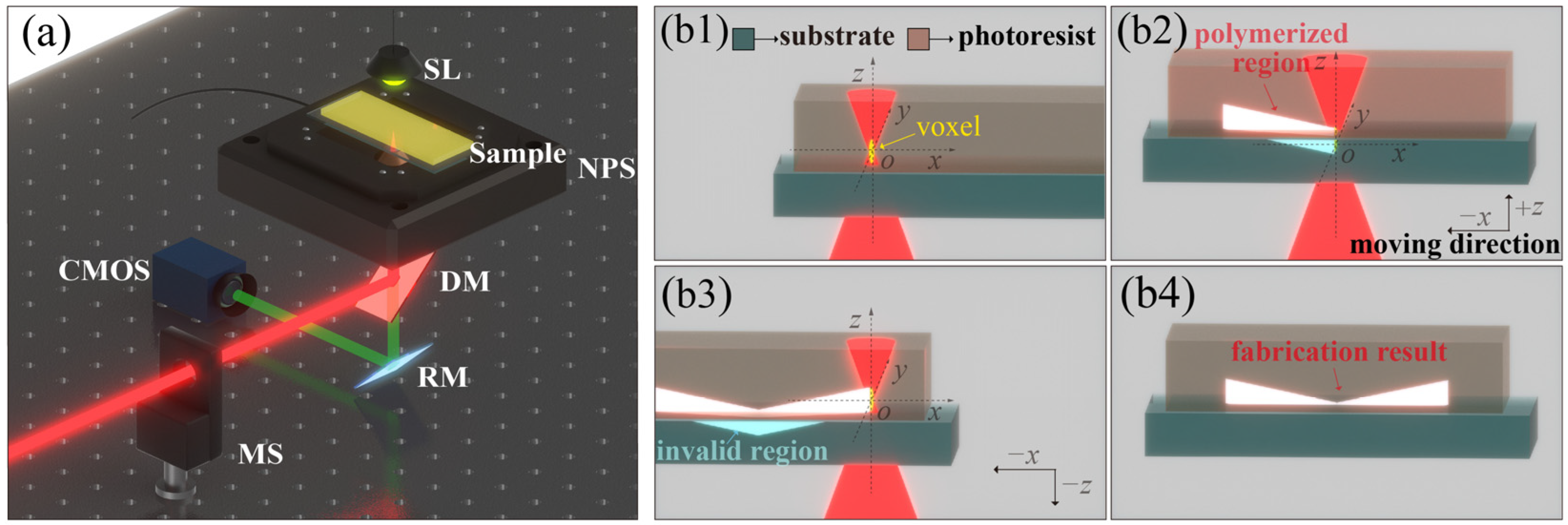
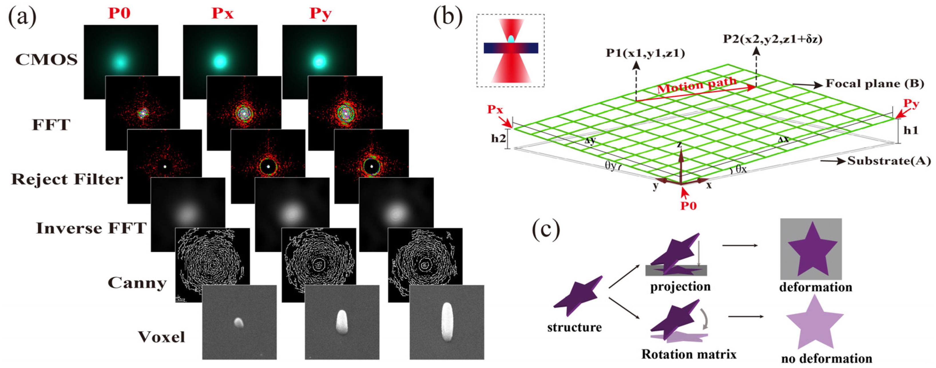
2.1. Setup and Fabrication Process

The TPP-LDW fabrication system is depicted in Figure 1a. In principle, TPP-LDW can be achieved with either a continuous laser [27] or a pulsed laser, as long as the photon density reaches the two-photon absorption threshold, and the concentration of the generated free radicals reaches the polymerization threshold. Typically, pulsed lasers, especially femtosecond lasers, are superior compared to continuous-wave lasers, for the two-photon absorption effect is more easily induced by the high peak power of pulsed lasers. Furthermore, the short pulse width minimizes the thermal effects of the processing area, which result in a higher processing accuracy. Therefore, femtosecond lasers are commonly chosen as the light source for TPP-LDW. This experimental system employed a femtosecond laser (Chameleon Ultra II, COHERENT, Saxonburg, PA, USA) with a tunable wavelength from 680 nm to 1080 nm, a pulse width of 140 fs, and a repetition frequency of 80 MHz. The TPP-LDW system uses 800 nm as the working wavelength due to its highest output power. Along the laser propagation path, a mechanical switch (MS) (SH05R/M, THORLABS, Newton, MA, USA), a dichroic mirror (DM) (DMSP605T, THORLABS) (800 nm HR), and a high-NA flat-field apochromatic objective lens (UPLXAPO100XO, OLYMPUS, Tokyo, Japan) were sequentially arranged. The nanoscale translation stage (NPS) (P-562.6CD, PHYSIK INSTRUMENTE, Karlsruhe, Germany) was used to control the spatial position of the photoresist-coated sample. A safe lamp (SL) at the visible band of 570–590 nm was used for wide-field illumination. The image on the objective focal plane was captured by a CMOS camera (MERCURY2, DAHENG IMAGING, Beijing, China) with the bridging of a reflection mirror (RM) (BB0511-E02, ZERODUR®, Mainz, Germany).
The photoresist used in this study contained 0.5 wt% 7-diethylamino-3-thenoylcoumarin (DETC, EXCITON, Lockbourne, OH, USA) initiator, and the monomer was pentaerythritol triacrylate (246794, SIGMA-ALDRICH, St. Louis, MI, USA). DETC is a commercial photoinitiator that is widely used for general and industrial purposes due to its high molar extinction coefficient and high intersystem crossing coefficient. The monomer (pentaerythritol triacrylate, PETA) from SIGMA-ALDRICH is a highly cross-linked negative photoresist monomer, which exhibits elevated mechanical strength after polymerization. In addition, the formulation and fabrication steps of the DETC-PETA photoresist are straightforward. In TPP-LDW processing, DETC molecules are excited to produce free radicals by simultaneously absorbing two 800 nm photons, which are equivalent to the energy of a 400 nm photon. This implies that for photoresists with a continuous absorption spectrum, the two-photon absorption band should be continuous as well.
The MNDNS fabrication process is illustrated in Figure 1(b1–b4). As shown in Figure 1(b1), at the beginning of the fabrication process, the TPP-LDW focus is located near the interface between the photoresist and the substrate, and the voxel size depends on the laser exposure time. Subsequently, the laser focus remains still, and the NPS platform starts to move along the negative x-axis and the positive z-axis directions simultaneously. As shown in Figure 1(b2), due to the two-photon polymerization effect, a polymerization region forms along the path of the voxel. As the NPS rises in the z-direction, the laser-processed voxel gradually sinks into the substrate, reducing the polymerization region and forming a smoothly transitioning needle structure. When the voxel is about to completely sink into the substrate, the NPS movement along the z-axis changes to the negative direction; then, the laser focus gradually rises from the substrate to fabricate a symmetric dual needle structure. Finally, the shutter is closed to complete the fabrication of MNDNS, and the fabricated structure is shown in Figure 1(b4).

2.2. Focus Self Compensation

However, in the TPP-LDW system with high numerical aperture (NA), the voxel size is extremely small. The lateral width of a voxel in TPP-LDW can change from a hundred nanometers to several hundred nanometers; this depends on many factors, such as laser power, exposure time, two-photon absorption cross section of the photo initiator, diffusion of radicals, numerical aperture of the objective, and so on [28]. While the axial width is usually 2- to 3-fold the lateral width [26]. Therefore, a slight angle change between the objective focal plane and the fabrication substrate may lead to issues such as structural deformation, tilting, or structural collapse while fabricating large-scale MNDNS. Suppose the maximum working range of the NPS is 200 μm, the axial width of the voxel is 2 μm, the center of the voxel is rightly located at the interface of the substrate and photoresist at the beginning of processing, and the angle formed by the focal plane and the NPS is α; therefore, the maximum fault angle that the processing could tolerate is α = ±arctan(1/200) = ±5 × 10⁻³ rad. The structure will be peeled off or wiped out from the substrate as the angle exceeds ±5 × 10⁻³ rad. The maximum fault angle is correlated with voxel size; therefore, it changes with the processing parameters. However, the axial width of the voxel is in the sub-micrometer to micrometer range, and the angle, which may influence the fabrication process, is generally at a magnitude of 10−3 rad.
Figure 2 illustrates the impact of the angle between the objective focal plane and the substrate during large-scale MNDNS fabrication. The laser power at the objective entrance pupil is 7.51 mW, the platform movement speed is 20 μm/s, the preset total length of the MNDNS is 100 μm, and the NPS height variation Δz is 0.6 μm. The MNDNS fabrication sequence is from ① to ⑧, with the platform moving along the positive x-axis direction. At the beginning of the fabrication, the voxel is located at the right endpoint of line 1, and the voxel center is located at the interface between the substrate and the photoresist. As shown in Figure 2a, with the above fabrication parameters, the desired dual needle structure of the MNDNS is not achieved. Furthermore, the left endpoints of lines ⑥, ⑦, and ⑧ are collapsed. This is because the substrate on the upper left side is lower than the objective focal plane. During MNDN fabrication, the inclined substrate fills the NPS movement distance along the z-direction, which keeps the laser focus always within the photoresist, thereby preventing formation of the dual needle structures. As the gap between the inclined substrate and the objective focal plane exceeds the scale in the z-axis direction of the voxel, the structure will detach from the substrate, resulting in structural collapse, as illustrated in Figure 2b.
The defocusing of the laser can be estimated by probing the inclination of the platform through laser spot variation during platform movement. Then, the levelness of the NPS can be amended by repeatedly adjusting the mechanical adjustable angle plate to finally become parallel the objective focal plane. However, this method is limited by the mechanical precision of the angle-adjustable device and the operator’s experience, making it difficult to ensure the fabrication accuracy and repeatability of MNDNS. Alternatively, an automatic focusing method could be applied for precise focus calibration. For example, Cao B. X. [29] incorporated a double-spot focus detection system into a laser processing system, which can provide real-time and accurate calculation of the defocusing distance. Subsequently, by controlling a negative lens moving back and forth along the axial direction of the processing optical path, the focal position can be adjusted dynamically to compensate for defocusing, according to the calculation results. However, such defocusing compensation methods in processing systems are relatively complex. Firstly, it requires the coupling of a double-spot detection optical path into the processing system, and it is prerequisite to precisely calibrating the detection optical path with the processing optical path. Additionally, it is necessary to insert a dynamically adjustable negative lens into the processing laser optical path to adjust the axial position of the focus, which also requires precise calibration of the negative lens’ moving distance with the focus shifting. In this study, we developed a fluorescence imaging analysis-assisted focus proactive compensating (FIAFPC) method. First, based on the fluorescence image of the photoresist captured by a CMOS camera, the tilt angle between the objective focal plane and the fabrication plan are quantitatively obtained. Then, utilizing the three-dimensional spatial transformation relationship between the two planes, the compensation amount of the voxel’s position on the fabrication path and the corrected platform running speed can be carried out. Finally, the nanomotion platform can execute corresponding position and speed control during fabrication to achieve accurate and automatic focus compensation.
In the FIAFPC method, the objective focal plane and the substrate plane are initially considered as two two-dimensional planes. To make the two planes coincide in space, it is necessary to measure the defocusing distance of the laser focus in the z-direction during the fabrication, and the rotation angle of the two planes in Euclidean space. Many photoresists can be excited to emit fluorescence through two-photon absorption. As the laser focus gradually shifts from the substrate into the photoresist resin, the photoresist produces a progressively enhanced fluorescence signal. The fluorescence signal is collected by a CMOS camera after passing through a dichroic mirror and a filter (800 nm band-stop filter). Since the intensity of the fluorescence is related to the spatial position of the laser focus in the z-direction, the depth of the current focus inside the photoresist can be inferred by analyzing the performance of the fluorescence intensity. As shown in Figure 3a, a series of fluorescence images is captured by the CMOS camera with the exposure parameter set as 100 ms. At the starting point of the objective focal plane, the image is captured as CMOS_P0; subsequently, images CMOS_Px and CMOS_Py are obtained by moving 200 μm along the x-axis and y-axis, respectively. In practical operation, CMOS_P0 is usually captured as the top of the laser focus just touches the bottom of the photoresist, and the morphology of the processed voxel at this moment is shown as Figure 3a—Voxel_P0. From the images, it can be observed that the fluorescence signal at positions Px and Py is stronger than that of the initial position, indicating an increased proportion of the laser focus entering the photoresist. The processed voxel morphologies at positions Px and Py are shown as Figure 3a Voxel_Px and Voxel_Py, respectively. The corresponding distribution of substrate plane A and objective focal plane B in TPP-LDW fabrication is shown in Figure 3b. To further determine the defocusing amount of the focus, the obtained fluorescence images are processed by frequency domain image enhancement FFT, followed by rejection of periodic noise within the specified range using a band-stop reject filter. Subsequently, inverse Fourier transforms are applied to convert the images into a grayscale image, and nonlinear high-pass filter with Canny edge detection is used to obtain the boundary of the maximum light intensity areas in the image. Finally, the NPS is used to precisely adjust the z-axis height until the edge detection pattern matches with that at the starting point of fluorescence image acquisition P0. As shown in Figure 3b, the differences at the edges of the two planes, h1 and h2, can be obtained. Subsequently, the angles that form between the axes of planes B and A ( θ x and θ y ) can be determined.
After determining the tilt of the plane, two methods can be used to compensate for the height difference and make the two planes coincide, which are the spatial projection method and the spatial path rotation method, respectively. As shown in Figure 3b, the projection method directly calculates the z-axis height that should be compensated for the fabricating point based on the plane slope. This method is easy to implement, but it can cause structural squeezing deformation when the tilt is severe. The spatial path rotation method uses position orientation description and a rotation matrix to achieve the relative rotation and translation of the entire fabrication path, thereby ensuring that the structures adhere to the substrate and maintain rotational invariance. Therefore, the spatial path rotation method is used to calculate the compensated path. For ease of description, the spatial Cartesian coordinate system {A} is used where the substrate is located, and the spatial Cartesian coordinate system {B} is used where the fabricating plane (focal plane) is located. Their unit vectors are given as follows:
A = x ^ A y ^ A z ^ A B = i ^ B j ^ B k ^ B
To describe the mapping of {B} relative to reference frame {A}, a rotation matrix R B A is introduced so that plane A can align with the substrate coordinates by multiplying this matrix, which is expressed as follows:
R B A = R R o l l c o s Head 0 s i n Head 0 1 0 s i n Head 0 c o s Head 1 0 0 0 c o s P i t c h s i n P i t c h 0 s i n P i t c h c o s P i t c h
where Head is θ y , Pitch is θ x , and Roll is 0, so the R R o l l matrix is the identity matrix E. To ensure rotational invariance and achieve compensation of the fabricating points in three-dimensional space, the modulated path P A matching the substrate coordinates can be obtained through left-multiplying the original fabricating path in the focal plane coordinate system P B by the rotation matrix R B A , i.e., the following:
P A = R B A P B
The components in the three-axial direction for each base vector of the modulated path are as follows:
P ^ n + 1 A P ^ n A = Δ P ^ x Δ P ^ y Δ P ^ z
To achieve coordination of the three axes to reach the target position at the same time, strict synchronization of the laser and platform spatial positions during fabrication is required. The piezoelectric translation stage must reach the predetermined positions in the x-, y-, and z-axis directions at the same time. For this purpose, the velocity components during the fabrication are orthogonally decomposed based on the direction of the piezoelectric translation stage, i.e., i B ^ and j B ^ . The z-axial velocity V z is calculated according to the travel time and assigned to the stage. The baseline speed V is the expected processing speed that can be set, and its magnitude directly affects the exposure time during processing, thereby changing the linewidth of the manufactured structure. After setting the baseline speed V and obtaining V x , V y through orthogonal decomposition, V z is assigned based on the travel time along either the x- or y-axis (also the waiting execution time for the nano-positioning stage). The velocity for each axis is shown in Formula (5).
V x = V Δ P x Δ P x 2 + Δ P y 2 V y = V Δ P y Δ P x 2 + Δ P y 2 V z = Δ P z Δ P x V x , Δ P x 0 Δ P z Δ P y V y , Δ P x 0
This proactive focus compensation method does not require additional leveling devices for the positioning platform.
To quantitatively understand the compensation accuracy of the FIAFPC, periodic linear structural processing is performed within the total working range of the NPS (200 μm × 200 μm). The interval of the structures is 5 μm, the laser power at the pupil is 8.04 mW, and the processing speed is 20 μm/s. After proactive compensation based on FIAFPC and determining the interface between the focus and the photoresist base, the NPS is moved downward by 0.3 μm as the starting position for processing. A Chinese character “正” is fabricated as a mark at specific locations, it serves as a square character for relative standards and is commonly used as a position marker for processing. Here, four square marks with a side length of 3 μm are manufactured at the four corners of the processing area, 50 μm away from the edges. The processing results are shown in Figure 4. Figure 4a is the overall SEM image of the linear structural array. It can be observed that the overall integrity of the line structure remains intact without any defocusing or misalignment. To determine the height variation information of the structure, AFM scans were performed at the position of the mark, obtaining three-dimensional morphological profiles at these specific locations Figure 4(b1–b4). From the height slice information, the maximum height is 307 nm, the minimum height is 240 nm, and the average height is h ¯ 272 nm. The standard deviation can be expressed as σ = 1 N i = 1 N ( h i h ¯ ) 2 = 21.07 . According to the structural profile from Figure 4(c1–c4), it is seen that the entire height of the structures in Figure 4(c2) is the highest, while the entire height of the structures in Figure 4(c3) is the lowest in the four AFM measuring areas. In other words, there is a slight angle between the processing plane and the objective plane with the FIAFPC. By dividing the height difference between the highest point P1 and the lowest point P2 in Figure 4(c2,c3), respectively, by the distance between them, the angle is approximately 4.65 × 10⁻⁴ rad, one order of magnitude less than the angle that may influence the fabrication process. The uncertainty primarily comes from two aspects: one is epistemic uncertainty in the relative height of the fluorescence imaging analysis substrate, and the other is aleatory uncertainty introduced by the movement of the NPS itself.

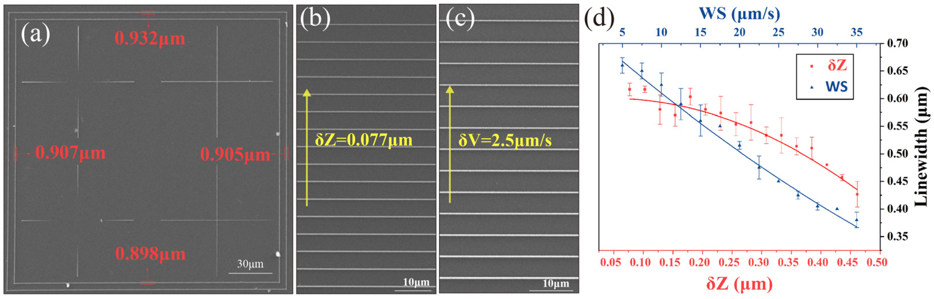
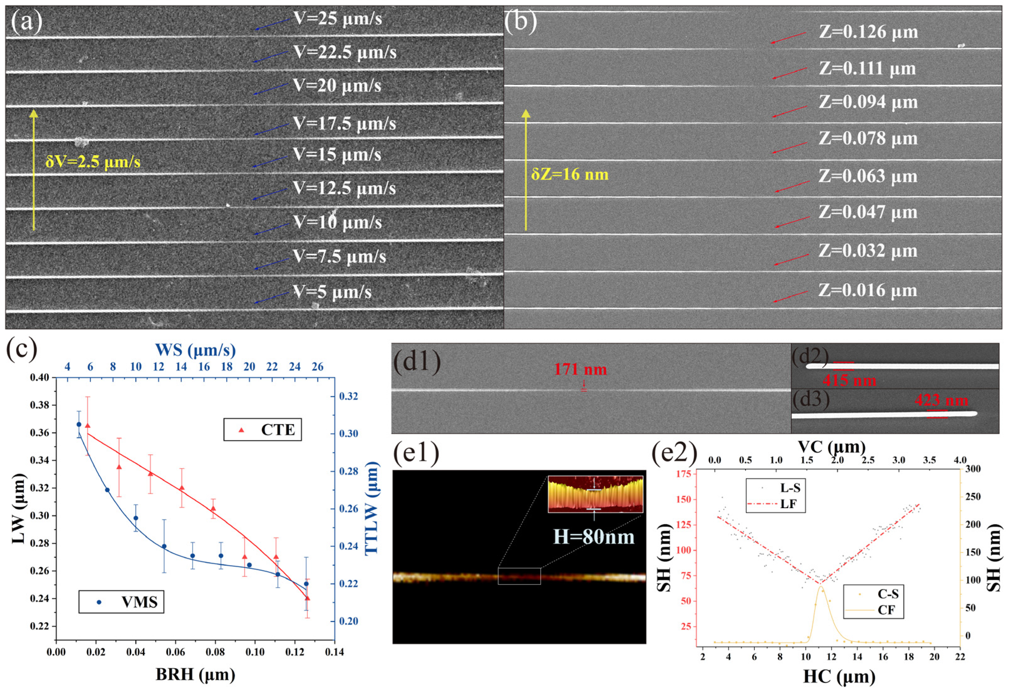
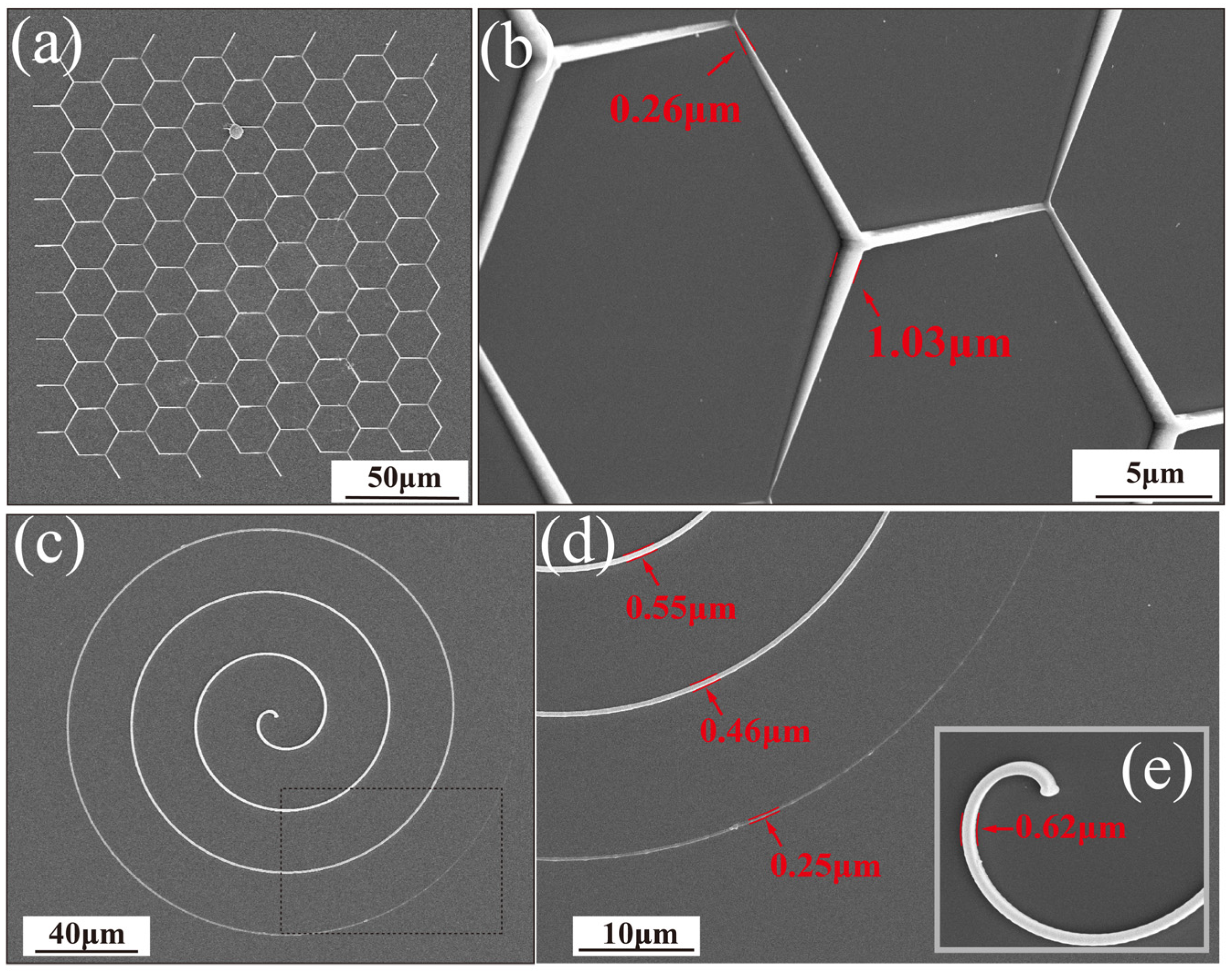
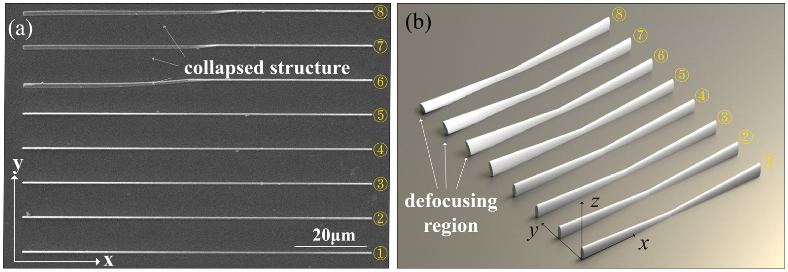
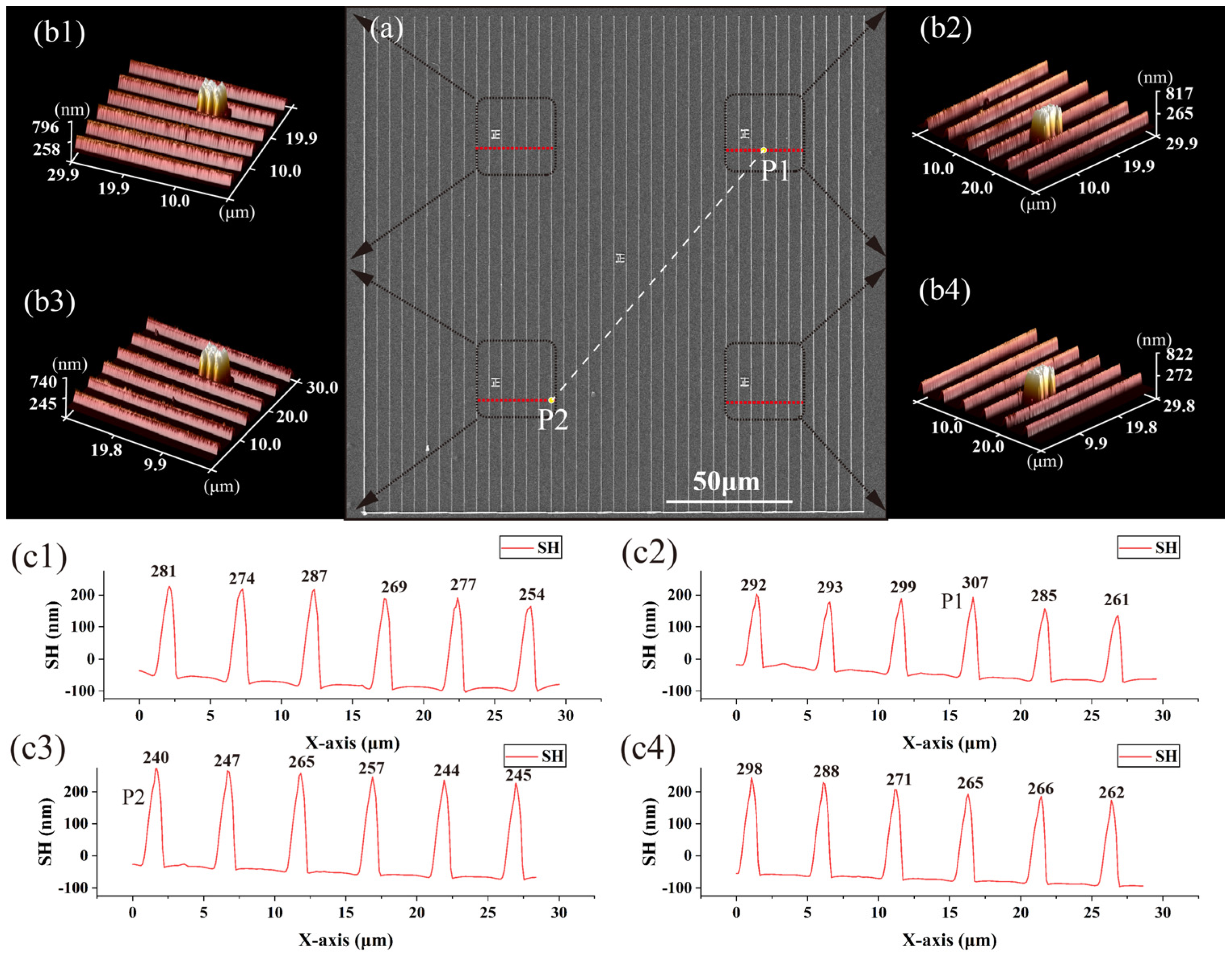
3. Results and Discussion

The results of large-scale micro/nano structure fabrication based on the FIAFPC method are shown in Figure 5a. The pupil laser power is 9.96 mW, the processing baseline speed is 20 μm/s, and the total processing range is the maximum movement range of the NPS (200 μm). The expected fabrication structures include two square frames, two cross-needle structures with morphology gradients, and two cross structures with different initial heights. As shown in Figure 5a, in the large-scale fabrication within 200 μm2, the FIAFPC method implemented proactive-dynamic compensation of the structures. The linewidth of processed structures is basically consistent, and the cross-structures are symmetric with respect to their centers. This indicates that the fabrication plane completely overlaps with the substrate; therefore, the polymer structure no longer suffers from defocusing issues due to the tilt angle between the focal plane and the substrate.
Figure 5b,c show the variations in the fabricating linewidth when the NPS height rose and the baseline speed increased, respectively. In Figure 5b, the laser pupil power is 7.78 mW, and the fabrication results are obtained by gradually raising the NPS height with a constant processing speed of 10 μm/s (the interface is located at the center of the voxel at the beginning of processing). In this case, the lifting of the NPS results in the gradual immersion of the focus into the glass substrate, so that the voxel involved in the exposure is reduced in morphology, thereby reducing the height and linewidth of the MNDNS. Meanwhile, Figure 5c represents the results obtained by changing the processing speed V without changing the height parameter and laser pupil power. Increasing the fabrication speed means reduction in the exposure, thus the linewidth of the processed structure decreases accordingly (the interface is located at the center of the voxel at the beginning of processing).
Figure 5d shows the linewidth measured using the particle size analysis software Nano Measurer. As can be seen from the existing calibration, either raising the NPS or increasing the fabrication speed could reduce the linewidth. The change in linewidth when raising the z-axis height is more pronounced, which is directly related to the elliptical shape of the voxel (the linewidth decreases rapidly when the substrate is close to the top end of the elliptical voxel). The increase in speed leads to a linear change in linewidth, which means the exposure dose depends linearly on the fabrication speed.
Similarly, the morphological features of MNDNS can be controlled by the processing speed and voxel position (NPS height). Figure 6a,b illustrate the results of MNDNS processing with variations in processing speed and NPS height when the entrance pupil power is constant (P = 7.78 mW). Figure 6a shows the MNDNS processing results with the fabrication starting position at the center of the voxel, and the processing speed gradually decreasing from 25 μm/s with a step size of 2.5 μm/s. Figure 6b shows the MNDNS processing results with the processing starting position at the center of the voxel, and the NPS height gradually decreasing from 0.016 μm. It can be observed that, based on the FIAFPC method, stable MNDNS can be obtained by controlling both processing speed and voxel position. Comparing the processing results of Figure 6a with Figure 6b, it is evident that the variation in the needle tip is more sensitive to the influence of voxel spatial position. The two needle parts are disconnected at the relative foundation height H = 0.826 μm. Figure 6c shows variations in linewidth at the tips of MNDNS with different fabrication speeds and voxel positions. The analysis of Figure 6c shows that with an increase in processing speed, the initial change in processing linewidth is relatively fast, and then gradually becomes slower. Theoretically, faster processing speeds are more advantageous for obtaining fine structures. However, in practical experiments, excessively high speeds often lead to fluctuations and defects in the processed structure, so it is essential to select an appropriate processing speed. Additionally, the greater variation in linewidth due to the gradual embedding of voxels into the substrate is determined by the ellipsoidal morphology of the voxels. Ultimately, with an entrance pupil power of 3.84 mW, fabrication speed of 22.5 μm/s, and a fabrication starting position at the voxel center, this research obtained a set of MNDNS with the minimum known tip width (as shown in Figure 6(d1)). The central linewidth reached 171 nm, and the widths at both ends were 415 nm and 423 nm, with a linewidth error of 1.91%. This illustrates that the FIAFPC method achieves high-precision proactive compensation with good symmetry for variable-size MNDNS. Figure 6(e1) shows scanning imaging results for the three-dimensional morphology and height information of the needle tip structure using AFM, which reveal the height changes in the needle tip. Figure 6(e2) shows the lateral profile of the minimum structure at the tip of the MNDNS obtained based on AFM scanning, along with the ridge structural profile of MNDNS. It can be observed that the ridge of the MNDNS approximates linear change that is determined by the characteristic voxel change in the z-direction, which is always linear. The fitted result of the longitudinal profile at the cone tip center is similar to the top morphology of the voxel, with a maximum height of 80.0 nm. The overall structure of the MNDNS is symmetrical, and its tip is perfectly aligned. The height at the center of the MNDNS depends on the extent to which the voxel is embedded in the substrate. The overall fabrication results in Figure 6 also confirm the accuracy of the proactive compensation method for the focal point proposed in this study. As shown in Figure 5 and Figure 6, processing MNDNS in a large range without defocusing is ultimately achieved through the processing and analysis of fluorescence images. This method allows us to obtain the defocus information of the entire MNDNS processing focal plane through a simple one-time calibration within the fabrication range, which subsequently ensures the accuracy and consistency of the processing results.
In addition, the FIAFPC method can be applied to the fabrication of more complex structures with continuously varying morphological gradients. In Figure 7a, a hexagon lattice structure was fabricated based on this method, where each hexagon is composed of three morphological gradient needle structures. In this lattice structure, the linewidth at the tip of each needle is approximately 0.260 μm, and the bottom linewidth is approximately 1.030 μm. The tips of every three micro/nanoneedles are connected to the same height feature point with the other two needles, ultimately creating a hexagon lattice structure with alternating heights. Figure 7c shows an Archimedean spiral structure with continuously graded height. Using the normal of the substrate plane as the axis of rotation and an arithmetic angle as the independent variable, the increasing radius angle of each processing point is 0.0275 rad relative to the previous point, while the radius increases two-fold over the current accumulated angle relative to the initial position, generating equidistant spiral curves. Meanwhile, the voxel evenly sinks into the substrate along the z-axis, and the overall height and linewidth of the spiral structure gradually decreases from the center of the pattern to the periphery. When processing gradient curve structures, all working axes of the NPS need to reach the target position simultaneously to ensure this in each subdivided processing step. It is necessary to recalculate the required velocities of each axis based on the compensated path. As the speeds of each axis need to dynamically change during the fabrication, the integrated program developed by this group is used to recursively calculate the speeds for each stage in advance, which are then pre-allocated in the NPS buffer to reduce the exposure offset caused by waiting during processing computation time. The focal point gradually penetrates the substrate along the spiral path relative to the substrate plane, and the fabrication linewidth also shrinks from 0.62 μm to 0.25 μm, or even narrower. The structures above can be replicated to obtain corresponding morphological gradient micro/nano channels through inverse molding, holding potential application value in micro/nano fluidics.
The advantages of the FIAFPC method are as follows: it does not require repeated adjustments of the NPS’s level, nor does it need to increase the complexity of the optical path. The position and velocity compensation of the laser focus in the processing can be obtained by analyzing the fluorescence images captured by the CMOS, and through rotational transformation. The compensation is achieved through the movement of the NPS platform. From the perspective of processing results, FIAFPC can effectively compensate for the defocusing problem in large-scale processing with inclined surfaces. However, the FIAFPC is a pre-compensation method. For processing surfaces that are curved or more complex, further research and improvements are needed.
These micro/nano functional structures with morphology gradients may hold potential application value in micro/nano fluidics studies. For example, in our previous research [30], a series of micro/nano channel arrays, which were obtained by molding micro/nano single needle structures, could be applied to investigate the translocation dynamics of T4-phage DNA through nanoconfinement.

4. Conclusions

This study proposes a novel fabricating method based on the coordinated movement of individual voxels and a high-precision nano platform. By adjusting the position of TPP-LDW voxels at the interface between the substrate and photoresist through high-precision movements of the nano platform, the method can achieve the fabrication of micro/nano structures with a gradient change in scale from sub-micrometer to nanometer levels. Simultaneously, a method for proactively compensating for the spatial position of fabricating points through fluorescence image analysis is proposed. The spatial and velocity compensation relationship of voxels was derived, which successfully addresses the issue of gradient structural deformation and collapse caused by the tilt angle between the focal plane and the sample during large-area processing of 200 μm × 200 μm sections. Subsequently, the effects of different fabricating speeds and voxel positions on the continuous gradient scaling of micro/nano dual needle structures were experimentally studied. Finally, with a total length of 200 μm, and the minimum height of 80 nm line and width of 171 nm at the tip structure were obtained. In addition, the methodology can also accurately construct hexagonal lattice periodic structures composed of size gradient triple needles and Archimedean spiral structures with size gradient changes. In addition, the proposed methodology can achieve precise production of complex gradient structures on a large scale with high spatial freedom and stability.

Author Contributions

Conceptualization, C.Z. and Z.W.; methodology, W.Z., Z.W. and J.B.; software, C.X.; validation, C.X. and Y.L.; analysis, C.Z. and C.X.; investigation, C.X.; resources, C.Z., B.L., K.W. and Z.W.; data curation, C.X. and Z.L.; writing—original draft preparation, C.X. and C.Z.; writing—review and editing, C.X., C.Z. and J.B.; visualization, C.X. and W.Z.; supervision, C.Z. and Z.W.; project administration, C.Z. and J.B.; funding acquisition, C.Z., B.L., K.W. and J.B. All authors have read and agreed to the published version of the manuscript.

Funding

This research was funded by the National Major Scientific Research Instrument Development Project of China (grant no. 51927804); the National Natural Science Foundation of China (grant nos. 62275216, 62375220); and the Science and Technology Innovation Team Project of Shaanxi Province (grant nos. S2018-ZC-TD-0061 and 2023-CX-TD-06).

Data Availability Statement

Data are contained within the article.

Conflicts of Interest

The authors declare no conflicts of interest.

References

  1. Duleba, D.; Johnson, R.P. Sensing with ion current rectifying solid-state nanopores. Curr. Opin. Electrochem. 2022, 34, 100989. [Google Scholar] [CrossRef]
  2. Zhou, Y.; Liao, X.; Han, J.; Chen, T.; Wang, C. Ionic current rectification in asymmetric nanofluidic devices. Chin. Chem. Lett. 2020, 31, 2414–2422. [Google Scholar] [CrossRef]
  3. Tu, Y.-M.; Samineni, L.; Ren, T.; Schantz, A.B.; Song, W.; Sharma, S.; Kumar, M. Prospective applications of nanometer-scale pore size biomimetic and bioinspired membranes. J. Membr. Sci. 2021, 620, 118968. [Google Scholar] [CrossRef]
  4. Chen, T.; Wang, D.; Chen, X.; Qiu, M.; Fan, Y. Three-dimensional printing of high-flux ceramic membranes with an asymmetric structure via digital light processing. Ceram. Int. 2022, 48, 304–312. [Google Scholar] [CrossRef]
  5. Ko, J.; Fredj, N.B.; Adhawiyah, R.E.; Lee, J. Nozzle-based precision patterning with micro-/nano fluidics integrated cantilevers. J. Mech. Sci. Technol. 2023, 37, 887–900. [Google Scholar] [CrossRef]
  6. Wang, D.; Abbas, Z.; Lu, L.; Liang, S.; Zhao, X.; Xu, P.; Zhao, K.; Suo, L.; Cui, Y.; Yin, P. Simulation of cone-jet and micro-drip regimes and printing of micro-scale patterns on PET substrate. Polymers 2022, 14, 2683. [Google Scholar] [CrossRef] [PubMed]
  7. Li, J.; Guo, Z. Spontaneous directional transportations of water droplets on surfaces driven by gradient structures. Nanoscale 2018, 10, 13814–13831. [Google Scholar] [CrossRef] [PubMed]
  8. Wen, T.; Zhang, C.; Gong, Y.; Liu, Z.; Zhao, W.; Zhan, Y.; Zhang, C.; Wang, K.; Bai, J. High-durability photothermal slippery surfaces for droplet manipulation based on ultraviolet lithography. Polymers 2023, 15, 1132. [Google Scholar] [CrossRef]
  9. Liu, Y.; Zhou, B.; Wang, W.; Shen, J.; Kou, W.; Li, Z.; Zhang, D.; Guo, L.; Lau, C.; Lu, J. Insertable, scabbarded, and nanoetched silver needle sensor for hazardous element depth profiling by laser-induced breakdown spectroscopy. ACS Sens. 2022, 7, 1381–1389. [Google Scholar] [CrossRef]
  10. Downs, A.M.; Bolotsky, A.; Weaver, B.M.; Bennett, H.; Wolff, N.; Polsky, R.; Miller, P.R. Microneedle electrochemical aptamer-based sensing: Real-time small molecule measurements using sensor-embedded, commercially-available stainless steel microneedles. Biosens. Bioelectron. 2023, 236, 115408. [Google Scholar] [CrossRef]
  11. Zhang, W.; Li, W.; Zhang, T.; Zheng, Z.; Chi, Z.; Jiang, Y.; Wu, N. A large-size and polarization-independent two dimensional grating fabricated by scanned reactive-ion-beam etching. Nanophotonics 2022, 11, 4649–4657. [Google Scholar] [CrossRef]
  12. Desbiolles, B.; Bertsch, A.; Renaud, P. Ion beam etching redeposition for 3D multimaterial nanostructure manufacturing. Microsyst. Nanoeng. 2019, 5, 11. [Google Scholar] [CrossRef] [PubMed]
  13. Saifullah, M.S.; Asbahi, M.; Neo, D.C.; Mahfoud, Z.; Tan, H.R.; Ha, S.T.; Dwivedi, N.; Dutta, T.; bin Dolmanan, S.; Aabdin, Z. Patterning at the resolution limit of commercial electron beam lithography. Nano Lett. 2022, 22, 7432–7440. [Google Scholar] [CrossRef] [PubMed]
  14. Lewis, S.M.; DeRose, G.A.; Alty, H.R.; Hunt, M.S.; Lee, N.; Mann, J.A.; Grindell, R.; Wertheim, A.; De Rose, L.; Fernandez, A. Tuning the performance of negative tone electron beam resists for the next generation lithography. Adv. Funct. Mater. 2022, 32, 2202710. [Google Scholar] [CrossRef]
  15. Tian, Y.; Polzer, F.B.; Zhang, H.V.; Kiick, K.L.; Saven, J.G.; Pochan, D.J. Nanotubes, plates, and needles: Pathway-dependent self-assembly of computationally designed peptides. Biomacromolecules 2018, 19, 4286–4298. [Google Scholar] [CrossRef] [PubMed]
  16. Ghosh, D.; Farahani, A.D.; Martin, A.D.; Thordarson, P.; Damodaran, K.K. Unraveling the self-assembly modes in multicomponent supramolecular gels using single-crystal X-ray diffraction. Chem. Mater. 2020, 32, 3517–3527. [Google Scholar] [CrossRef]
  17. Huang, S.; Zhang, Q.; Xin, P.; Zhang, J.; Chen, Q.; Fu, J.; Jin, Z.; Wang, Q.; Hu, Z. Construction of Fe-doped NiS–NiS2 heterostructured microspheres via etching prussian blue analogues for efficient water-urea splitting. Small 2022, 18, 2106841. [Google Scholar] [CrossRef]
  18. Khanna, S.; Paneliya, S.; Ray, A.; Mukhopadhyay, I.; Banerjee, R. Controlled etching of silica nanospheres monolayer for template application: A systematic study. Appl. Surf. Sci. 2020, 500, 144050. [Google Scholar]
  19. Chen, S.-T.; Huang, C.-T.; Zheng, M.-Y.; Yen, H.-Y. Co-shaft in-situ rolling-imprinting technique for printing of silver micro-nanowire array. J. Mater. Process. Technol. 2022, 299, 117387. [Google Scholar] [CrossRef]
  20. Cox, L.M.; Martinez, A.M.; Blevins, A.K.; Sowan, N.; Ding, Y.; Bowman, C.N. Nanoimprint lithography: Emergent materials and methods of actuation. Nano Today 2020, 31, 100838. [Google Scholar] [CrossRef]
  21. Ding, H.; Zhang, Q.; Gu, Z.; Gu, M. 3D computer-aided nanoprinting for solid-state nanopores. Nanoscale Horiz. 2018, 3, 312–316. [Google Scholar] [CrossRef] [PubMed]
  22. Cao, Q.; Shin, M.; Lavrik, N.V.; Venton, B.J. 3D-printed carbon nanoelectrodes for in vivo neurotransmitter sensing. Nano Lett. 2020, 20, 6831–6836. [Google Scholar] [CrossRef] [PubMed]
  23. Faraji Rad, Z.; Nordon, R.E.; Anthony, C.J.; Bilston, L.; Prewett, P.D.; Arns, J.-Y.; Arns, C.H.; Zhang, L.; Davies, G.J. High-fidelity replication of thermoplastic microneedles with open microfluidic channels. Microsyst. Nanoeng. 2017, 3, 1–11. [Google Scholar] [CrossRef] [PubMed]
  24. Cordeiro, A.S.; Tekko, I.A.; Jomaa, M.H.; Vora, L.; McAlister, E.; Volpe-Zanutto, F.; Nethery, M.; Baine, P.T.; Mitchell, N.; McNeill, D.W. Two-photon polymerisation 3D printing of microneedle array templates with versatile designs: Application in the development of polymeric drug delivery systems. Pharm. Res. 2020, 37, 1–15. [Google Scholar] [CrossRef] [PubMed]
  25. Plamadeala, C.; Gosain, S.R.; Hischen, F.; Buchroithner, B.; Puthukodan, S.; Jacak, J.; Bocchino, A.; Whelan, D.; O’Mahony, C.; Baumgartner, W. Bio-inspired microneedle design for efficient drug/vaccine coating. Biomed. Microdevices 2020, 22, 1–9. [Google Scholar] [CrossRef] [PubMed]
  26. Zhang, C.; Hou, J.Q.; Lin, J.Q.; Li, K.; Fan, L.B.; Zhang, C.; Wang, K.G.; Bai, J.T. Investigation on fabricating continuous gradient micro/nano needle structure by single Femtosecond laser voxel (Invited). Acta Photonica Sinica 2022, 51, 1014001. [Google Scholar]
  27. Thiel, M.; Fischer, J.; Von Freymann, G.; Wegener, M. Direct laser writing of three-dimensional submicron structures using a continuous-wave laser at 532 nm. Appl. Phys. Lett. 2010, 97, 221102. [Google Scholar] [CrossRef]
  28. Sun, H.-B.; Takada, K.; Kim, M.-S.; Lee, K.-S.; Kawata, S. Scaling laws of voxels in two-photon photopolymerization nanofabrication. Appl. Phys. Lett. 2003, 83, 1104–1106. [Google Scholar] [CrossRef]
  29. Cao, B.X.; Le, P.H.; Ahn, S.; Kang, H.; Kim, J.; Noh, J. Automatic real-time focus control system for laser processing using dynamic focusing optical system. Opt. Express 2017, 25, 28427–28441. [Google Scholar] [CrossRef]
  30. Zhang, C.; Hou, J.; Zeng, Y.; Dai, L.; Zhao, W.; Jing, G.; Sun, D.; Cao, Y.; Zhang, C. An optically fabricated gradient nanochannel array to access the translocation dynamics of T4-phage DNA through nanoconfinement. Lab Chip 2023, 23, 3811–3819. [Google Scholar] [CrossRef]
Figure 1. Fabrication method for morphological gradient micro/nano structure variants. (a) Schematic of TPP-LDW experimental setup. (b1b4) Illustration of the MNDNS fabrication process.
Photonics 11 00187 g001
Figure 2. Influence of the angle between the objective focal plane and the substrate plane on the fabrication of MNDNS. (a) SEM characterization of the fabricated results. (b) Schematic diagram of the angle impact on MNDNS.
Photonics 11 00187 g002
Figure 3. Procedure of FIAFPC method. (a) Fluorescence image processing workflow in FIAFPC and corresponding voxel morphology. (b) Schematic of fluorescence image acquisition points and the spatial distribution of objective focal plane (focal plane B) and substrate (substrate A). (c) Principle of proactive compensation of focus using spatial projection method and rotation matrix method.
Photonics 11 00187 g003
Figure 4. Processing results of periodic linear structures over a 200 μm × 200 μm area based on FIAFPC. (a) Overall SEM image of the fabricated structures (the red dotted lines show the locations of cross-sectional sampling for AFM). (b1b4): AFM images of the linear structure morphology around specific marks. (c1c4): Cross-sectional sampling of the linear structures in (b1b4). FIAFPC: fluorescent image analysis-based proactive compensation method, AFM: atomic force microscope, SH: structure height.
Photonics 11 00187 g004
Figure 5. Results of large-scale micro/nano structure fabricating based on FIAFPC. (a) Results of large-scale fabricating. (b) Results of NPS position gradient fabricating (lifting step size is 0.077 μm). (c) Results of NPS velocity gradient processing (velocity change step size is 2.5 μm/s). (d) Influence of voxel position and working speed on fabricating linewidth (WS: working speed).
Photonics 11 00187 g005
Figure 6. Analysis of the fabrication results of micro/nano dual needle structures with morphological gradient based on (a) different fabrication speeds (baseline speed 5–25 μm) and (b) different NPS heights (z-axis change step 0.016 μm) with a power of P = 7.78 mW at the pupil (lifting height of foundation is 0.7 μm). (c) variations in linewidth at the tips of MNDNS with different fabrication speeds and voxel positions. (d1) SEM image of the smallest MNDNS. (d2,d3) Structural morphology at the two ends of the dual needle. (e1) AFM image of the dual needle structure (detailed view of the needle tip inside the dashed box). (e2) AFM contour analysis of the needle tip structure. WS: working speed; LW: linewidth; TTLW: taper tip linewidth; VC: vertical coordinates; SH: structure height; HC: horizontal coordinates; L-S: longitudinal section; LF: linear fitting; C-S: cross-section; CF: cubic fit.
Photonics 11 00187 g006
Figure 7. Fabrication of controllable gradient structures based on the FIAFPC method. (a) Periodic lattice structure composed of scale gradient micro/nano-needle arrays (P = 6.03 mW, V = 20 μm/s, the relative height change at each feature point from the starting point is 0.75 μm). (b) Local zoom-in image of Figure (a). (c) Fabrication of Archimedean spiral structure with height and linewidth gradient (P = 4.52 mW, combined speed of V = 10 μm/s, overall height change is 0.75 μm). (d) The zoomed-in area of black dashed box of Figure (c). (e) Detailed view of the starting point of the Archimedean spiral structure.
Photonics 11 00187 g007
Disclaimer/Publisher’s Note: The statements, opinions and data contained in all publications are solely those of the individual author(s) and contributor(s) and not of MDPI and/or the editor(s). MDPI and/or the editor(s) disclaim responsibility for any injury to people or property resulting from any ideas, methods, instructions or products referred to in the content.

