1. Introduction
Thanks to the impressive progress in microelectronic technology over the last decade, integrated photonics has taken on an irreplaceable role in the transmission and management of data, as it allows transmission speeds and information processing capabilities unattainable with any other technology [
1,
2]. Photonic switches, which under appropriate electrical commands are capable of routing an optical signal among N destinations, are indispensable components in modern optical communication networks, appreciated for their high speed and low latency [
3,
4,
5,
6].
Unlike their electronic counterparts, photonic switches offer the advantage of low power consumption and a wide bandwidth. These features are especially vital as data rates continue to increase and the limitations of electronic switching become more pronounced. The miniaturization of photonic switches on silicon platforms has further promoted their adoption, leveraging the established silicon photonics technology. This technology is enabled by compatibility with existing semiconductor manufacturing processes and allows micro-scale and cost-effective devices, paving the way for large-scale deployment. This integration also facilitates the creation of compact, monolithic photonic circuits which can be seamlessly incorporated into existing electronic microchips, allowing the design and fabrication of electronic-photonic hybrid devices with capabilities not achievable otherwise [
7,
8].
Photonic switches are usually based on Mach–Zehnder interferometers (MZIs) [
9,
10] or multimode interference devices (MMIs) [
11,
12]. Both approaches have been widely adopted due to their ability to manipulate light effectively. The physical mechanism for selective routing typically involves the use of electro-optical [
13,
14] or thermo-optical effects [
15,
16], which alter the refractive index of the material within the switch. When an electrical signal is applied, it induces a change in the refractive index of the waveguide or in a limited region of it, causing light to be directed to a specific output port. Unfortunately, both of these devices also present specific drawbacks, particularly in terms of wavelength selectivity and polarization sensitivity [
17,
18,
19], which might prevent their deployment in cases where multiple carrier wavelengths are present in a given band, and the whole band should be routed toward one out of N outputs. A sample case is that of wavelength division multiplexing (WDM), which is adopted in the C and L bands in passive optical networks (PONs) [
20].
A valid approach to the design of non-wavelength-selective photonic devices is that of exploiting adiabatic principles. In these devices, a gradual change in the refractive index profile allows light to remain in its fundamental mode throughout the transitions regardless of wavelength and polarization, thus providing more robust and reliable performances [
21,
22,
23,
24,
25]. This gradual evolution minimizes diffusion losses and ensures efficient mode conversion, making adiabatic devices highly efficient.
In this work, we present what we believe to be the first design of a simple integrated photonic switch based on silicon-on-insulator (SOI) technology which utilizes adiabatic transition principles coupled to the thermo-optic effect to produce digital optical switching while maintaining consistent performances across a wide wavelength range (1525–1625 nm) for both TE and TM polarizations. The device design features narrow cross-section ridge waveguides, which enable effective light confinement and switching. Our study demonstrates that in spite of the compactness targets of micro-photonics, the refractive index distribution within the structure can be efficiently modified through localized heating [
26].
2. Theory
In general, a physical process can be assumed to be adiabatic if it takes place in a sufficiently slow manner such that there are no transitions between energy levels. This principle can be translated into the integrated optics domain by assuming that the propagating modes do not change even if the waveguide structure changes along the optical path. This means that if a given mode (e.g., the fundamental one) is initially excited, then all power remains in that mode as the waveguide geometry changes. No power is coupled to other modes or radiated into the continuum. The advantage of adiabatic devices in integrated optics is that there are no critical dimensions required to achieve optimal performance, such as the length of a resonator or a directional coupler. Therefore, adiabatic devices exhibit low wavelengths and polarization dependence. This also implies more relaxed constraints in terms of technology for their fabrication. However, they generally have the disadvantage of being longer. For example, an asymmetric Y-splitter (−3 dB) can be made adiabatic if the angle between the two branches is sufficiently small, as Equation (1) shows [
27,
28]:
where Δ
β is the difference in the propagation constant between the two lowest-order normal modes when the arms of the branch are separated well and
γ is the transverse propagation constant in the cladding region between arms. It turns out that the design of short devices implies either large splitting between the two modes or strong coupling between the waveguides (low γ values). Such devices work well even when the technology used for fabrication has large minimum feature sizes, although this implies longer tapers. Using smaller minimum feature sizes could lead to shorter devices. For example, a coupling length down to 5 µm was demonstrated in the case of an adiabatic power splitter with a 30 nm minimum feature size [
29].
In this paper, based on numerical simulations, we present the design of an adiabatic passive splitter and subsequently verify its functionality as an active switch by introducing a refractive index perturbation across its geometry induced by the thermo-optic effect. The resulting temperature profile directs optical radiation toward one of the two otherwise balanced outputs. The primary objectives are to achieve a sufficiently large operational bandwidth and high efficiency for both TE and TM fundamental propagating modes.
3. Design of the Passive Splitter
The adiabatic structure is shown in
Figure 1, though not to scale. It consists of a rectangular cross-section waveguide at the input, three parallel tapered waveguides, and two S-bent waveguides at the output. The structure is fabricated in silicon (n = 3.4732) with SiO
2 under- and overcladding. It follows the design of a passive adiabatic Y-splitter [
21] but with modifications; the central waveguide has a rectangular cross-section, while the two outer waveguides include thin slabs (100 nm) at their outer sides. These slabs are essential for enhancing heat diffusion from nearby heaters, which are positioned far enough away to avoid disturbing the propagating optical field. The main geometrical parameters of the design are summarized in
Table 1.
The Si waveguides have a thickness of 310 nm, which aligns with some current technology standards [
30] and ensures good propagation performance for both the TE and TM modes.
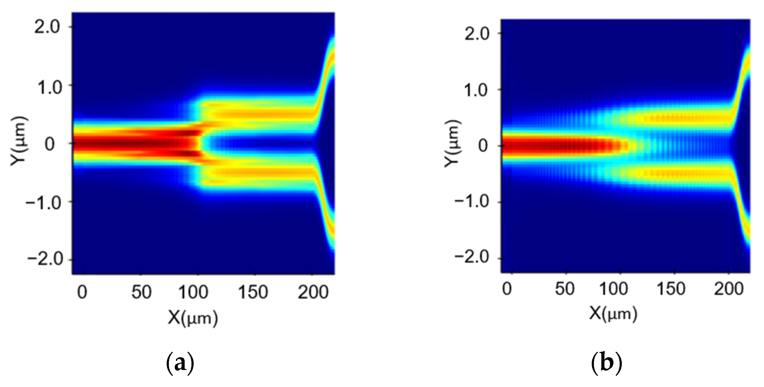
At a uniform temperature of 300 K, the device is a symmetric splitter. This behavior is demonstrated in
Figure 2, which displays the electric field propagation for the TE and TM modes in a device with L
t = 100
m. The transmitted radiation at each output is −3.20 ± 0.02 dB over the whole considered wavelength range.
4. Thermo-Optic Switch and Simulation Results
4.1. Thermal Simulation
Starting from the passive splitter described above, steady state thermal simulations were conducted using a 2D heat propagation numerical solver [
30] to assess the temperature distribution produced when a specified amount of heat was applied to one of the 100 nm-thick lateral titanium (Ti) heaters. The thermal parameters used in the simulations are provided in
Table 2, including the thermo-optic coefficients of silicon (Si), silicon dioxide (SiO
2), and Ti. The handle layer of the SOI platform was considered at a constant temperature of 300 K, while the lateral boundaries were adiabatic. The top SiO
2 cladding was exposed to air, where heat was removed by convection. The ambient temperature was 300 K.
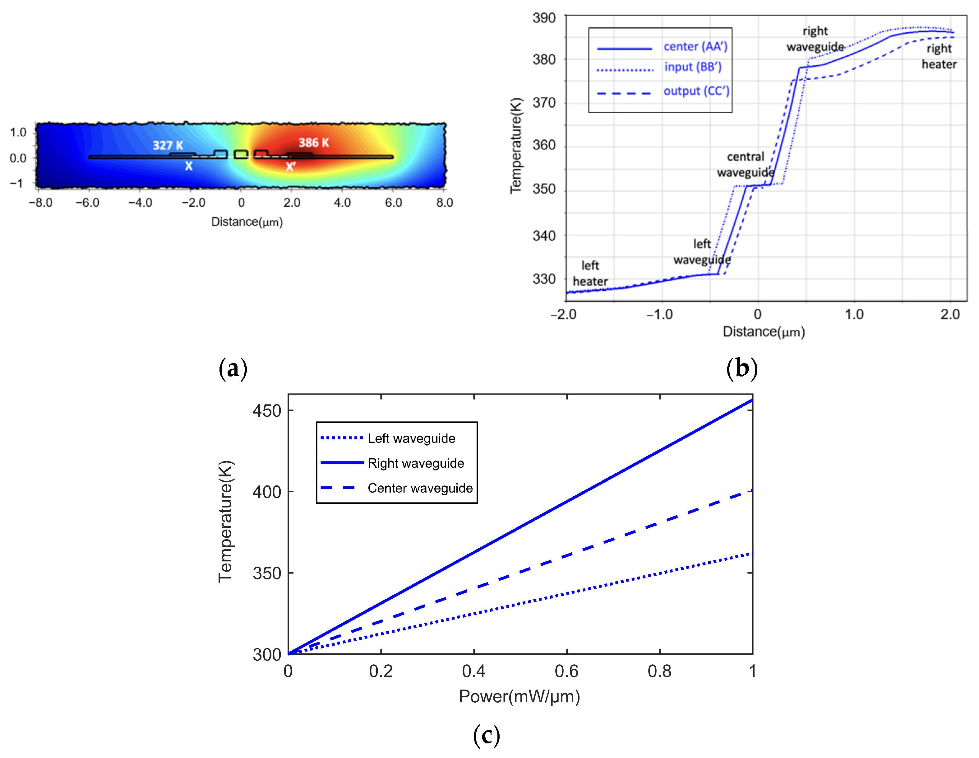
Figure 3a illustrates the temperature distribution at half the length of the switch (section A-A’ of
Figure 1) when a power dissipation of 0.5 mW per unit length (µm) was applied to the heater on the right side.
Figure 3b shows the calculated temperature profile across the X-X’ cut line at half the length of the three tapered regions under the same power input of 0.5 mW/
m.
Figure 3c shows the temperature of the three waveguides as a function of the applied power. It can be seen that due to the high thermal conductivity of silicon, each waveguide was in fact isothermal. The temperature profiles were passed to the quasi-3D finite-difference time domain (FDTD) simulator [
31] to compute the propagating optical field. The results were also verified through eigenmode expansion (EME) simulations, which provided comparable results.
Table 2.
Thermal properties of materials.
Table 2.
Thermal properties of materials.
| Material | Thermal Conductivity
(W/m·K) | Thermo-Optic Coefficient (K−1) |
|---|
| Silicon (Si) | 148 [32] | 2.01 × 10⁻⁴ [33] |
| Silicon dioxide (SiO2) | 1.38 [34] | 8.4 × 10⁻⁶ [35] |
| Titanium (Ti) | 11.4 [36] | 3.7 × 10⁻⁴ [37] |
4.2. Optical Simulation
For varying applied power levels,
Figure 4 illustrates how extending the length of the tapered waveguides from 50 µm to 250 µm significantly impacted the extinction ratio (ER) for both the TE and TM modes across the full wavelength range. In particular, the graphs shows that a taper length of 50 µm was too short for obtaining a high ER for both the TE and TM modes. Specifically, with an applied power of 1 mW/µm, for the TE mode, the ER increased from 1.05 dB to 12.15 dB at a wavelength of 1.525 µm and from 1.9 dB to 20.33 dB at 1.625 µm. For the TM mode, the ER rose from 5.8 dB to 19.64 dB at 1.525 µm and from 7.36 dB to 14.27 dB at 1.625 µm as the waveguide length increased. The impact of varying the power applied to the lateral heater up to a maximum of 1 mW/µm, a practical level for thermo-optic switches, is also evident in the graphs.
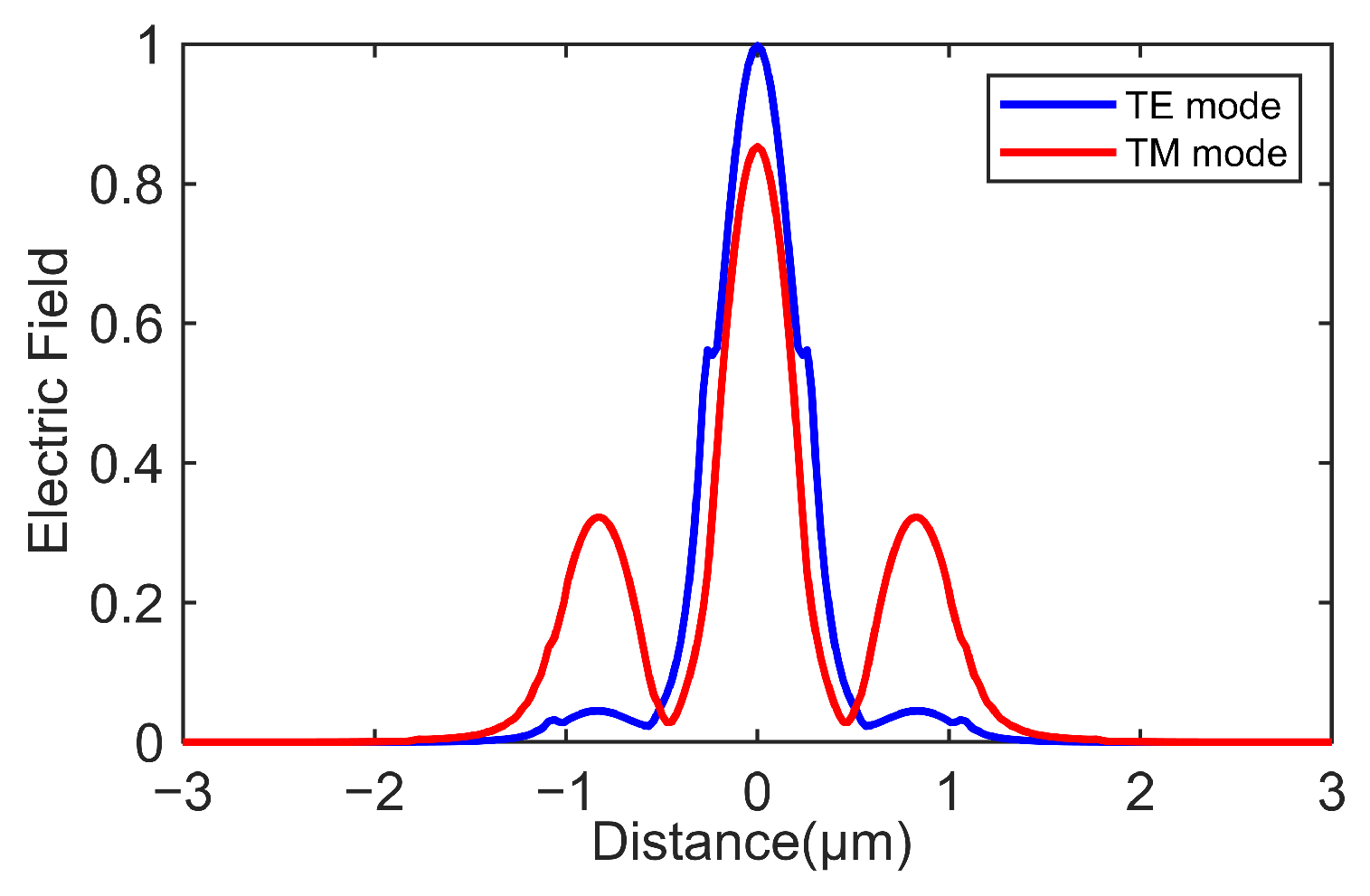
It is noteworthy that for a taper length L
t of 100 µm and an input heating power of 1 mW/µm, the switch demonstrated a high extinction ratio (ER) for the TM mode at both wavelengths. In contrast, the TE mode required taper lengths exceeding 200 µm to achieve a comparable performance. This behavior arose from the stronger confinement of the TE mode compared with the TM mode, as illustrated in
Figure 5. The figure presents the electric field profile along the X-X’ cutline of
Figure 3a for both modes at λ = 1550 nm and an applied power of 0 mW/µm.
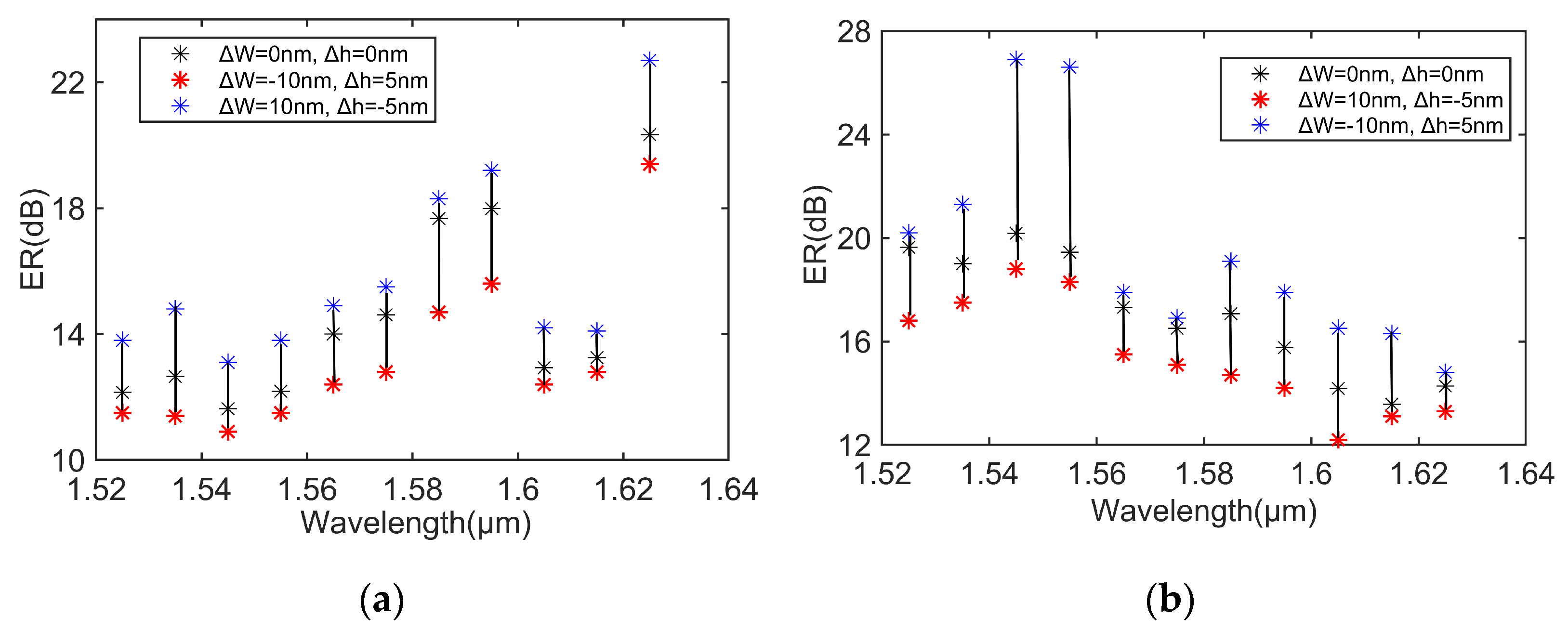
Figure 6 displays the extinction ratios (ERs) across different wavelengths for both the TE and TM modes when the taper length was 250 µm. The average ER values were 14.25 dB and 17 dB for the TE and TM modes, respectively. The ER values reported here were also calculated while considering fabrication tolerance effects, including a ΔW = ±10 nm error for the waveguide width and a Δh = ±5 nm for the Si thickness [
38]. For the TE mode, the best-case scenario corresponded to ΔW = +10 nm and Δh = −5 nm, whereas the worst-case scenario was ΔW = −10 nm and Δh = +5 nm. Conversely, the opposite behavior was observed for the TM mode. The device’s insertion losses (ILs) were estimated by measuring the optical power loss between the device’s input and output. Thanks to the high transparency of undoped silicon in the wavelength range of interest and a waveguide thickness of 310 nm, the average insertion loss (IL) values remained low. Specifically, the IL was 0.37 dB for the TE mode and 0.52 dB for the TM mode across the entire specified wavelength range, excluding coupling losses.
A comparison of our adiabatic digital optical switch with similar devices is presented in
Table 3. The listed devices include Mach–Zehnder switches (MZSs) and multi-mode interference (MMI) switches. The comparison reveals that while the ER of the proposed device was comparable to those of other thermo-optic switches, it also had a wide bandwidth, good extinction ratio, and compactness. Additionally, it had the advantage of operating in both TE and TM modes. Aside from this, the choice of an adiabatic structure naturally made the device less sensitive to temperature fluctuations, which might affect the response of devices relaying in interferential or resonance phenomena instead. For the proposed device, the higher the temperature differences between the external tapered waveguides, the higher the ER. At 1 mW/μm, this difference was larger than 100 K, which is enough to prevent effects from ambient temperature fluctuations. That aside, the substrate can be held in the case of a relatively constant temperature by means of an active heat sink.
5. Conclusions
We investigated a thermo-optic switch capable of operating for both polarizations. The device exploits the advantages of an adiabatic design with tapered waveguides to perform flat responses across the C and L bands of optical communications. With an overall length of 250 µm and power dissipation of 1 mW/µm, the switch achieved extinction ratios of 12.15 dB and 20.33 dB for the TE mode at wavelengths of 1.525 µm and 1.625 µm, respectively, and 19.64 dB and 14.27 dB for the TM mode at the same wavelengths. The switch exhibited low insertion losses with average values of 0.37 dB and 0.52 dB for the TE and TM modes, respectively.
This study demonstrates that adiabatic structures on silicon-on-insulator platforms are highly effective for thermo-optic switching applications, providing a robust solution for integrated optical systems. Additionally, the ability to fine-tune parameters such as the waveguide thickness, taper length, and gap distance allows for optimal performance and flexibility across a range of applications.
The proposed device can be easily fabricated using standard integrated photonic technology and is well suited for applications in broadband optical communication architectures. Its high reliability and polarization independence make it particularly advantageous for wavelength-division multiplexed passive optical networks (WDM-PONs) in fiber-to-the-home (FTTH) infrastructures.
Author Contributions
Conceptualization, B.H., F.G.D.C.; methodology, B.H., M.C., T.C., M.M., F.G.D.C.; simulations, B.H.; writing: B.H.; verification: B.H., M.C., T.C., M.M.; supervision, F.G.D.C. All authors have read and agreed to the published version of the manuscript.
Funding
This work was partially supported by the European Union under the Italian National Recovery and Resilience Plan (NRRP) of the NextGenerationEU partnership for “Telecommunications of the Future” (PE00000001—program “RESTART”—FP5 GraPHICs).
Institutional Review Board Statement
Not applicable.
Informed Consent Statement
Not applicable.
Data Availability Statement
The data presented in this study are available on request from the corresponding author. The data are not publicly available due to privacy reasons.
Conflicts of Interest
The authors declare no conflicts of interest.
References
- Wang, J.; Long, Y. On-chip silicon photonic signaling and processing: A review. Sci. Bull. 2018, 63, 1267–1310. [Google Scholar] [CrossRef] [PubMed]
- Asghari, M.; Krishnamoorthy, A.V. Energy-efficient communication. Nat. Photonics 2011, 5, 268–270. [Google Scholar] [CrossRef]
- Farmakidis, N.; Youngblood, N.; Lee, J.S.; Feldmann, J.; Lodi, A.; Li, X.; Aggarwal, S.; Zhou, W.; Bogani, L.; Pernice, W.H.; et al. Electronically reconfigurable photonic switches incorporating plasmonic structures and phase change materials. Adv. Sci. 2022, 9, 2200383. [Google Scholar] [CrossRef]
- Yu, R.; Cheung, S.; Li, Y.; Okamoto, K.; Proietti, R.; Yin, Y.; Yoo, S.J.B. A scalable silicon photonic chip-scale optical switch for high performance computing systems. Opt. Express 2013, 21, 32655–32667. [Google Scholar] [CrossRef] [PubMed]
- Hirokawa, T.; Saeidi, M.; Pillai, S.; Nguyen-Le, A.; Theogarajan, L.; Saleh, A.A.M.; Schow, C.L. A wavelength-selective multiwavelength ring-assisted Mach–Zehnder interferometer switch. J. Light. Technol. 2020, 38, 6292–6298. [Google Scholar] [CrossRef]
- Yoo, S.J.B. Photonic switching technologies, architectures, and integrated-systems for future disaggregated and optically reconfigurable data centers. In Proceedings of the 2022 International Conference on Optical Network Design and Modeling (ONDM), Warsaw, Poland, 16–19 May 2022; IEEE: New York, NY, USA, 2022. [Google Scholar]
- Moazeni, A.H.A.S.; Pavanello, F.; Gevorgyan, H.; Notaros, J.; Alloatti, L.; Wade, M.T.; Sun, C.; Kruger, S.A.; Meng, H.; Al Qubaisi, K.; et al. Integrating photonics with silicon nanoelectronics for the next generation of systems on a chip. Nature 2018, 556, 349–354. [Google Scholar]
- Absil, P.P.; Verheyen, P.; De Heyn, P.; Pantouvaki, M.; Lepage, G.; De Coster, J.; Van Campenhout, J. Silicon photonics integrated circuits: A manufacturing platform for high density, low power optical I/O’s. Opt. Express 2015, 23, 9369–9378. [Google Scholar] [CrossRef]
- Kumar, S.; Raghuwanshi, S.K.; Kumar, A. Implementation of optical switches using Mach–Zehnder interferometer. Opt. Eng. 2013, 52, 097106. [Google Scholar] [CrossRef]
- Guo, Z.; Lu, L.; Zhou, L.; Shen, L.; Chen, J. 16 × 16 Silicon Optical Switch Based on Dual-Ring-Assisted Mach–Zehnder Interferometers. J. Light. Technol. 2017, 36, 225–232. [Google Scholar] [CrossRef]
- Nagai, S.; Morishima, G.; Inayoshi, H.; Utaka, K. Multimode interference photonic switches (MIPS). J. Light. Technol. 2004, 20, 675–681. [Google Scholar] [CrossRef]
- Jia, X.; Luo, S.; Cheng, X. Design and optimization of novel ultra-compact SOI multimode interference optical switch. Opt. Commun. 2008, 281, 1003–1007. [Google Scholar] [CrossRef]
- Hashemi, B.; Keihani, M.; Alizadeh, A.H. Design, simulation of XOR/XNOR and AND logic gates using the optical two-circle switch. Opt. Contin. 2022, 1, 399–408. [Google Scholar] [CrossRef]
- Van Campenhout, J.; Green, W.M.J.; Assefa, S.; Vlasov, Y.A. Low-power, 2 × 2 silicon electro-optic switch with 110-nm bandwidth for broadband reconfigurable optical networks. Opt. Express 2009, 17, 24020–24029. [Google Scholar] [CrossRef] [PubMed]
- Watts, M.R.; Sun, J.; DeRose, C.; Trotter, D.C.; Young, R.W.; Nielson, G.N. Adiabatic thermo-optic Mach–Zehnder switch. Opt. Lett. 2013, 38, 733–735. [Google Scholar] [CrossRef]
- Song, L.; Lyu, L.; Jiao, X.; Gao, C.; Liu, W.; Li, H.; Shi, Y.; Dai, D. Low-Loss C+L+S-Band 2 × 2 Thermo-Optic Mach-Zehnder Switches with Compact Fast Quasi-Adiabatic Couplers. J. Light. Technol. 2024, 42, 8316–8322. [Google Scholar] [CrossRef]
- Robinson, M.G.; Johnson, K.M.; Doroski, D. Polarization-independent, broadband, bistable, 2 × 2 optical exchange switch. Opt. Lett. 1990, 15, 145–147. [Google Scholar] [CrossRef] [PubMed]
- Sun, X.; Feng, J.; Zhong, L.; Lu, H.; Han, W.; Zhang, F.; Akimoto, R.; Zeng, H. Silicon nitride based polarization-independent 4 × 4 optical matrix switch. Opt. Laser Technol. 2019, 119, 105641. [Google Scholar] [CrossRef]
- Wang, H.; Dai, J.; Jia, H.; Shao, S.; Fu, X.; Zhang, L.; Yang, L. Polarization-independent tunable optical filter with variable bandwidth based on silicon-on-insulator waveguides. Nanophotonics 2018, 7, 1469–1477. [Google Scholar] [CrossRef]
- Wey, J.S. The outlook for PON standardization: A tutorial. J. Light. Technol. 2019, 38, 31–42. [Google Scholar] [CrossRef]
- Ozcan, C.; Mojahedi, M.; Aitchison, J.S. Short, broadband, and polarization-insensitive adiabatic Y-junction power splitters. Opt. Lett. 2023, 48, 4901–4904. [Google Scholar] [CrossRef]
- Queraltó, G.; Ahufinger, V.; Mompart, J. Integrated photonic devices based on adiabatic transitions between supersymmetric structures. Opt. Express 2018, 26, 33797–33806. [Google Scholar] [CrossRef]
- Fu, Y.; Ye, T.; Tang, W.; Chu, T. Efficient adiabatic silicon-on-insulator waveguide taper. Photonics Res. 2014, 2, A41–A44. [Google Scholar] [CrossRef]
- Khan, S.; Buckley, S.M.; Chiles, J.; Mirin, R.P.; Nam, S.W. Low-loss, high-bandwidth fiber-to-chip coupling using capped adiabatic tapered fibers. APL Photonics 2020, 5, 056101. [Google Scholar] [CrossRef]
- Ozcan, C.; Aitchison, S.; Mojahedi, M. Foundry-Processed Compact and Broadband Adiabatic Optical Power Splitters with Strong Fabrication Tolerance. Photonics 2023, 10, 1310. [Google Scholar] [CrossRef]
- Cocorullo, G.; Della Corte, F.G.; Rendina, I. Temperature dependence of the thermo-optic coefficient in crystalline silicon between room temperature and 550 K at the wavelength of 1523 nm. Appl. Phys. Lett. 1999, 74, 3338–3340. [Google Scholar] [CrossRef]
- Burns, W.K.; Milton, A.F. Mode conversion in planar-dielectric separating waveguides. IEEE J. Quantum Electron. 1975, 11, 32–39. [Google Scholar] [CrossRef]
- Shani, Y.; Henry, C.; Kistler, R.; Kazarinov, R.; Orlowsky, K. Integrated optic adiabatic devices on silicon. IEEE J. Quantum Electron. 1991, 27, 556–566. [Google Scholar] [CrossRef]
- Wang, Y.; Gao, S.; Wang, K.; Skafidas, E. Ultra-broadband and low-loss 3 dB optical power splitter based on adiabatic tapered silicon waveguides. Opt. Lett. 2016, 41, 2053–2056. [Google Scholar] [CrossRef]
- CEA-LETI Photonics. Available online: https://europractice-ic.com/technologies/photonics/cea-leti/ (accessed on 7 December 2024).
- Lumerical Inc. Available online: https://www.ansys.com/products/optics/ (accessed on 7 December 2024).
- Volz, S.G.; Chen, G. Molecular-dynamics simulation of thermal conductivity of silicon crystals. Phys. Rev. 2000, 61, 2651. [Google Scholar] [CrossRef]
- Frey, B.J.; Leviton, D.B.; Madison, T.J. Temperature-dependent Refractive Index of Silicon and Germanium. Optomech. Technol. Astron. 2006, 6273, 62732J. [Google Scholar]
- Brotzen, F.; Loos, P.; Brady, D. Thermal conductivity of thin SiO2 films. Thin Solid Film. 1992, 207, 197–201. [Google Scholar] [CrossRef]
- Gao, H.; Jiang, Y.; Cui, Y.; Zhang, L.; Jia, J.; Jiang, L. Investigation on the Thermo-Optic Coefficient of Silica Fiber Within a Wide Temperature Range. J. Light. Technol. 2018, 36, 5881–5886. [Google Scholar] [CrossRef]
- Klemens, P.G.; Williams, R.K. Thermal conductivity of metals and alloys. Int. Met. Rev. 1986, 31, 197–215. [Google Scholar] [CrossRef]
- Gülşen, G.; Inci, M.N. Thermal optical properties of TiO2 films. Opt. Mater. 2002, 18, 373–381. [Google Scholar] [CrossRef]
- Dwivedi, S.; D’heer, H.; Bogaerts, W. Maximizing fabrication and thermal tolerances of all-silicon FIR wavelength filters. IEEE Photonics Technol. Lett. 2015, 27, 871–874. [Google Scholar] [CrossRef]
- Yue, J.; Wang, M.; Zou, J.; Liu, T.; Fang, J.; Sun, X.; Wu, Y.; Zhang, D. Low-loss silica waveguide 1 × 8 thermo-optic switch based on large-scale multimode interference couplers. Opt. Commun. 2024, 573, 131014. [Google Scholar] [CrossRef]
- Wang, M.; Yue, J.; Yao, Z.; Liu, T.; Sun, X.; Wu, Y.; Zhang, D. Low-power and wide-band 1 × 8 silica waveguide optical switch. Opt. Laser Technol. 2024, 171, 110380. [Google Scholar] [CrossRef]
- Wang, S.; Dai, D. Polarization-insensitive 2 × 2 thermo-optic Mach–Zehnder switch on silicon. Opt. Lett. 2018, 43, 2531–2534. [Google Scholar] [CrossRef]
- Chen, Q.; Wang, M.K.; Ma, X.X.; Yao, H.; Chen, K.X. Broadband and low-random-phase-errors 2 × 2 optical switch on thin-film lithium niobate. IEEE Photonics J. 2022, 14, 1–5. [Google Scholar] [CrossRef]
- Li, W.; Xu, L.; Zhang, J.; Mao, D.; D’Mello, Y.; Wei, Z. Broadband polarization-insensitive thermo-optic switches on a 220-nm silicon-on-insulator platform. IEEE Photonics J. 2022, 14, 1–7. [Google Scholar] [CrossRef]
- Chen, T.; Ding, Z.; Dang, Z.; Jiang, X.; Zhang, Z. Function-versatile thermo-optic switch using silicon nitride waveguide in polymer. Photonics 2023, 10, 277. [Google Scholar] [CrossRef]
- Jin, M.; Wu, G.; Zhou, X.; Jiang, Q.; Lin, Z.; Jiang, W. Parabolic MMI coupler for 2 × 2 silicon optical switch with robustly high extinction ratio for four paths. IEEE Photonics Technol. Lett. 2023, 35, 737–740. [Google Scholar] [CrossRef]
| Disclaimer/Publisher’s Note: The statements, opinions and data contained in all publications are solely those of the individual author(s) and contributor(s) and not of MDPI and/or the editor(s). MDPI and/or the editor(s) disclaim responsibility for any injury to people or property resulting from any ideas, methods, instructions or products referred to in the content. |
© 2024 by the authors. Licensee MDPI, Basel, Switzerland. This article is an open access article distributed under the terms and conditions of the Creative Commons Attribution (CC BY) license (https://creativecommons.org/licenses/by/4.0/).

 ,
, 

