Threshold Gain Reduction in Tandem Semiconductor Nano-Lasers


Abstract
1. Introduction
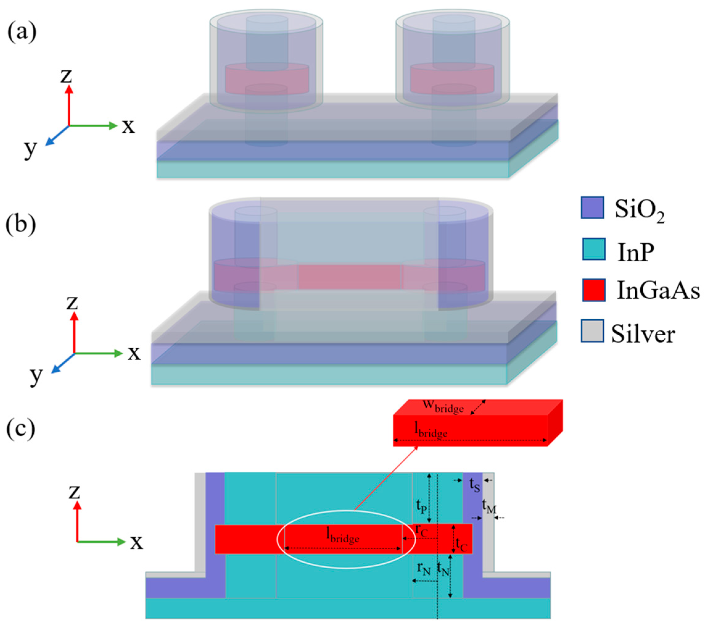
2. Model
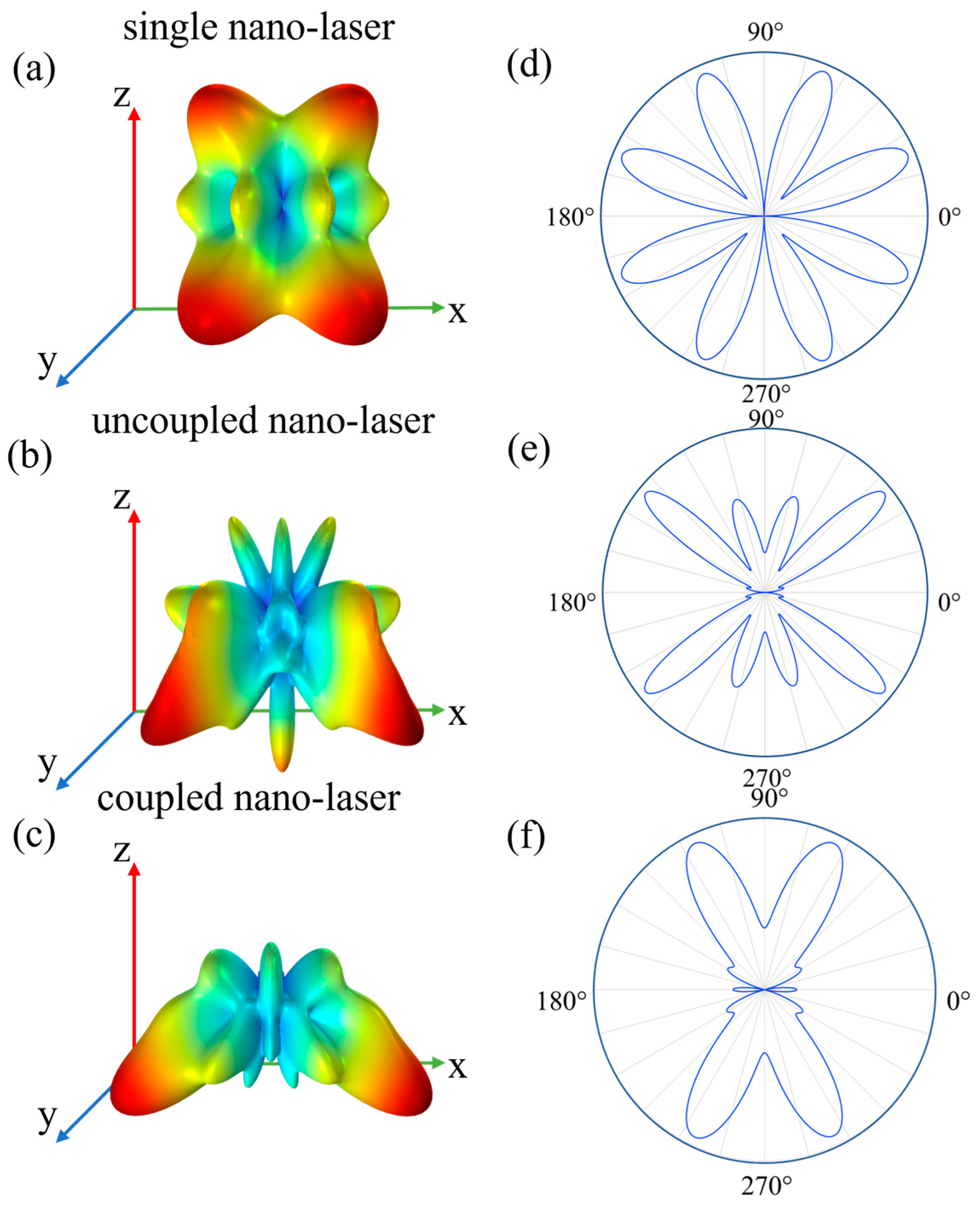
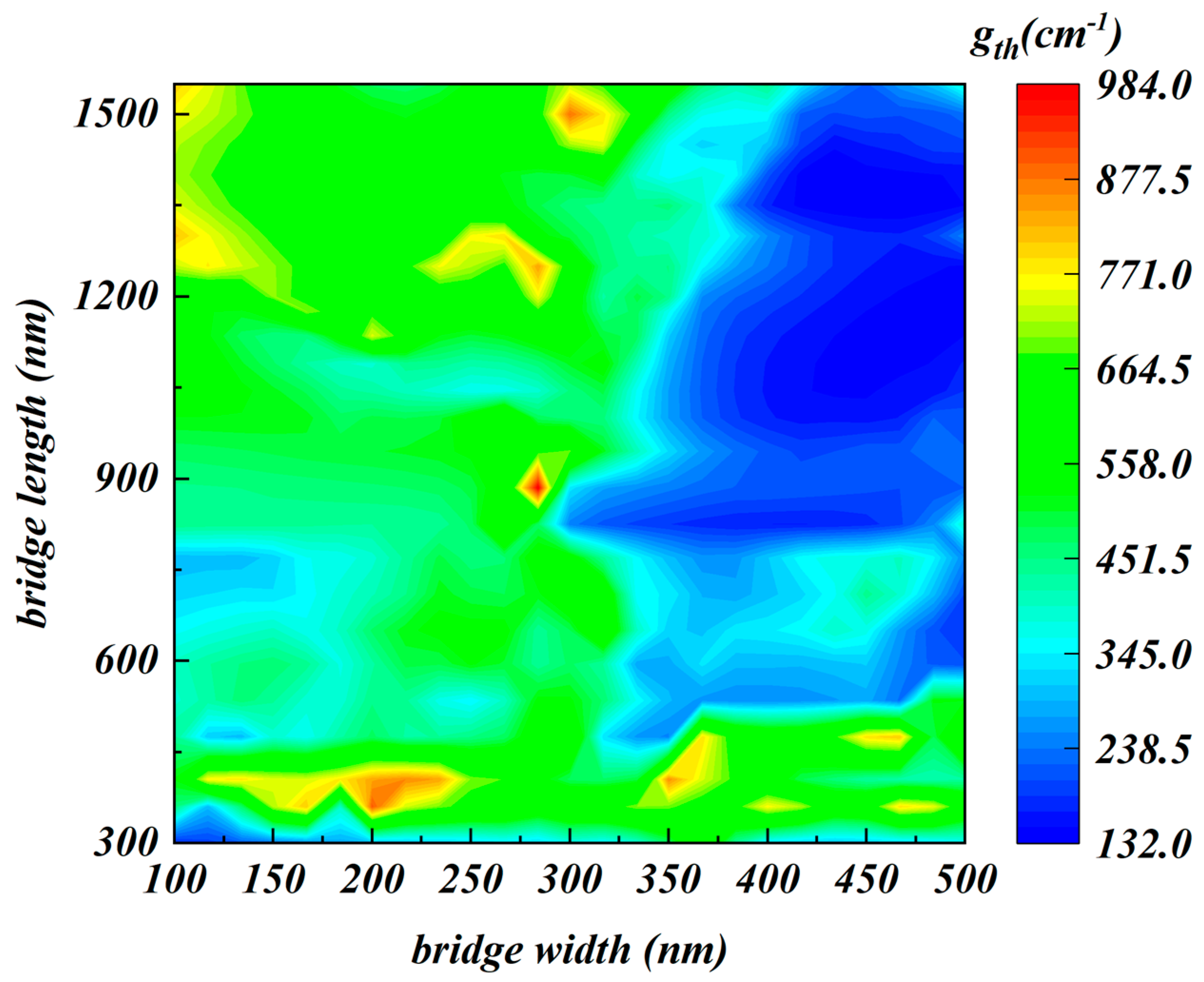
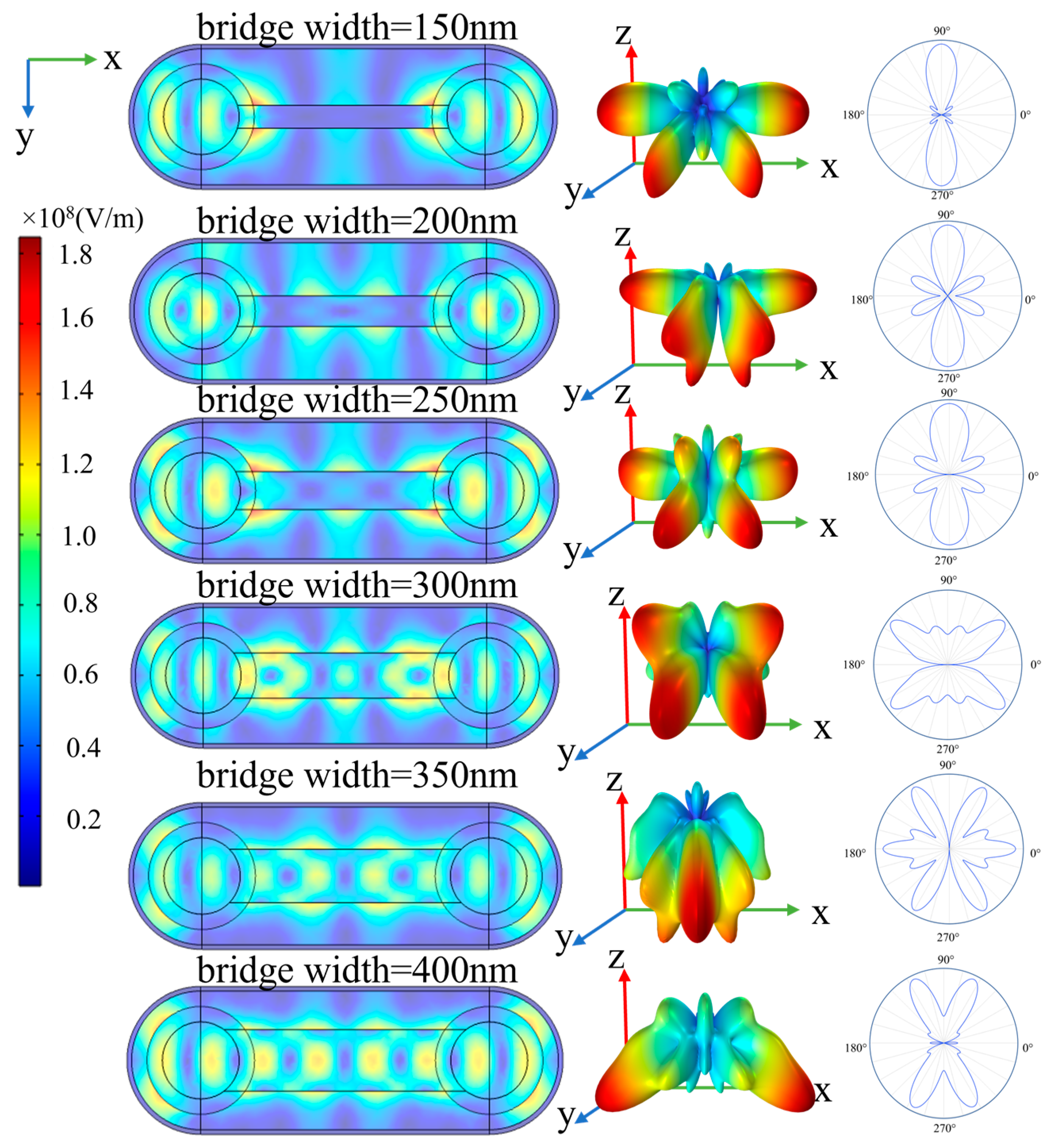
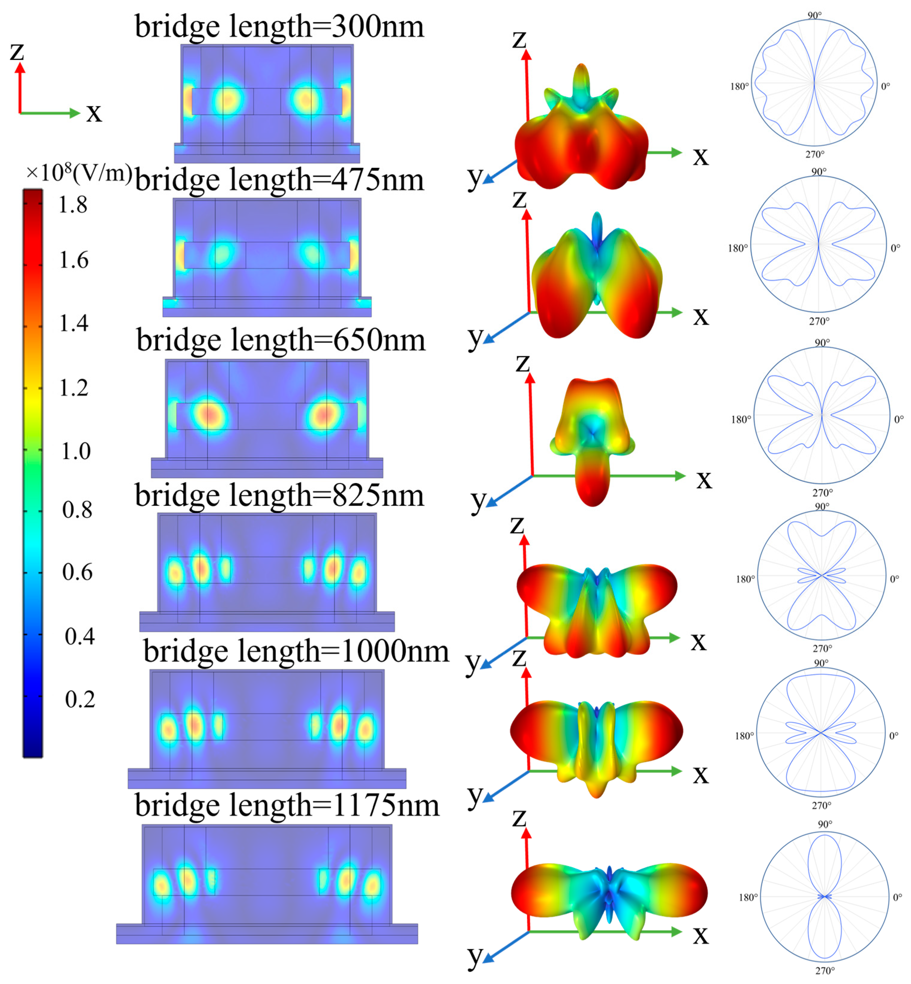
3. Results
4. Conclusions
Author Contributions
Funding
Data Availability Statement
Conflicts of Interest
References
- Ding, K.; Hill, M.T.; Liu, Z.C.; Yin, L.J.; Van Veldhoven, P.J.; Ning, C.Z. Record Performance of Electrical Injection Sub-Wavelength Metallic-Cavity Semiconductor Lasers at Room Temperature. Opt. Express 2013, 21, 4728. [Google Scholar] [CrossRef] [PubMed]
- Gu, Q.; Shane, J.; Vallini, F.; Wingad, B.; Smalley, J.S.T.; Frateschi, N.C.; Fainman, Y. Amorphous Al2O3 Shield for Thermal Management in Electrically Pumped Metallo-Dielectric Nanolasers. IEEE J. Quantum Electron. 2014, 50, 499–509. [Google Scholar] [CrossRef]
- Li, K.H.; Liu, X.; Wang, Q.; Zhao, S.; Mi, Z. Ultralow-Threshold Electrically Injected AlGaN Nanowire Ultraviolet Lasers on Si Operating at Low Temperature. Nat. Nanotechnol. 2015, 10, 140–144. [Google Scholar] [CrossRef] [PubMed]
- Ren, K.; Li, C.; Fang, Z.; Feng, F. Recent Developments of Electrically Pumped Nanolasers. Laser Photonics Rev. 2023, 17, 2200758. [Google Scholar] [CrossRef]
- Fan, Y.; Shore, K.A. Design of Room Temperature Electrically Pumped Visible Semiconductor Nanolasers. IEEE J. Quantum Electron. 2018, 54, 2000907. [Google Scholar] [CrossRef]
- Han, H.; Shore, K.A. Dynamical Characteristics of Nano-Lasers Subject to Optical Injection and Phase Conjugate Feedback. IET Optoelectronics 2017, 12, 25–29. [Google Scholar] [CrossRef]
- Fan, Y.; Hong, Y.; Li, P. Numerical Investigation on Feedback Insensitivity in Semiconductor Nanolasers. IEEE J. Sel. Top. Quantum Electron. 2019, 25, 1–7. [Google Scholar] [CrossRef]
- Fan, Y.; Shore, K.A.; Shao, X. Dynamics of Electrically Pumped Semiconductor Nano-Laser Arrays. Photonics. 2023, 10, 1249. [Google Scholar] [CrossRef]
- Fan, Y.; Shi, T.; Zhang, J.; Shore, K.A. Optical Injection Effects in Electrically Pumped Semiconductor Nano-laser Arrays. Opt. Express 2024, 32, 19361–19371. [Google Scholar] [CrossRef] [PubMed]
- Deka, S.S.; Pan, S.H.; Gu, Q.; Fainman, Y.; El Amili, A. Coupling in a dual metallo-dielectric nanolaser system. Opt. Lett. 2017, 42, 4760–4763. [Google Scholar] [CrossRef] [PubMed]
- Zhang, B.; Zhu, K.; Hao, J.; Wang, B.; Shen, Z.; Hu, H. Design and Numerical Study of Semiconductor Nanolaser with Gaussian-Shaped Metallic Cavity. IEEE Photonics J. 2018, 10, 4502110. [Google Scholar] [CrossRef]
- Peng, X.; Liu, J.; Kang, Y.; Mao, X.; Yan, W.; Wang, X.; Liu, K.; Xu, R.; Yang, F.; Li, Z. Coupling of Photonic and Plasmonic Modes for Double Nanowire Cavities. Photonics. 2023, 10, 415. [Google Scholar] [CrossRef]
- Shane, J.; Gu, Q.; Potterton, A.; Fainman, Y. Effect of Undercut Etch on Performance and Fabrication Robustness of Metal-Clad Semiconductor Nanolasers. IEEE J. Quantum Electron. 2015, 51, 2000109. [Google Scholar] [CrossRef]
- Palik, E.D. Handbook of Optical Constants of Solids; Academic Press: London, UK, 1985. [Google Scholar]


| Layer Name | Material | Size |
|---|---|---|
| InGaAs Core | InGaAs | tC = 300 nm, rC = 350 nm |
| N Doped Layer | N InP | tN = 450 nm, rN = 250 nm |
| P Doped Layer | P InP | tP = 470 nm |
| Insulating Layer | SiO2 | tS = 100 nm |
| Metal Layer | Ag | tM = 30 nm |
| Bridge | InGaAs | lbridge = variable, wbridge = variable |
Disclaimer/Publisher’s Note: The statements, opinions and data contained in all publications are solely those of the individual author(s) and contributor(s) and not of MDPI and/or the editor(s). MDPI and/or the editor(s) disclaim responsibility for any injury to people or property resulting from any ideas, methods, instructions or products referred to in the content. |
© 2024 by the authors. Licensee MDPI, Basel, Switzerland. This article is an open access article distributed under the terms and conditions of the Creative Commons Attribution (CC BY) license (https://creativecommons.org/licenses/by/4.0/).
Share and Cite
Fan, Y.; Zhang, J.; Shore, K.A. Threshold Gain Reduction in Tandem Semiconductor Nano-Lasers. Photonics 2024, 11, 1037. https://doi.org/10.3390/photonics11111037
Fan Y, Zhang J, Shore KA. Threshold Gain Reduction in Tandem Semiconductor Nano-Lasers. Photonics. 2024; 11(11):1037. https://doi.org/10.3390/photonics11111037
Chicago/Turabian StyleFan, Yuanlong, Jing Zhang, and K. Alan Shore. 2024. "Threshold Gain Reduction in Tandem Semiconductor Nano-Lasers" Photonics 11, no. 11: 1037. https://doi.org/10.3390/photonics11111037
APA StyleFan, Y., Zhang, J., & Shore, K. A. (2024). Threshold Gain Reduction in Tandem Semiconductor Nano-Lasers. Photonics, 11(11), 1037. https://doi.org/10.3390/photonics11111037