Article

High-Efficiency and High-Monochromaticity Semitransparent Organic Solar Cells Based on Optical Tamm States

by
Junwei Zhao
1,
Senxuan Lin
1,
Jinxin Zhou
1,
Fuhao Gao
1,
Jingfeng Liu
1,
Yongbing Long
1,2,3 and
Haitao Xu
1,*
1
College of Electronic Engineering/College of Artificial Intelligence, South China Agricultural University, Guangzhou 510642, China
2
Lingnan Modern Agr Sci & Technol Guangdong Lab, Guangzhou 510642, China
3
Natl Ctr Int Collaborat Res Precis Agr Aviat Pest, South China Agricultural University, Guangzhou 510642, China
*
Author to whom correspondence should be addressed.
Photonics 2024, 11(11), 1030; https://doi.org/10.3390/photonics11111030
Submission received: 4 October 2024 / Revised: 20 October 2024 / Accepted: 23 October 2024 / Published: 1 November 2024
(This article belongs to the Special Issue Recent Advances in Micro/Nano-Optics and Photonics)

Abstract

:
Semitransparent organic solar cells (ST-OSCs) have garnered more interest and stand out as promising candidates for next-generation solar energy harvesters with their unique advantages. However, challenges remain for the advancement of colorful ST-OSCs, such as enhancing the light absorption and transmittance without considerable power conversion efficiency (PCE) losses. Herein, an optical analysis of silver (Ag) electrodes and one-dimensional photonic crystals (1DPCs) was conducted by simulations, revealing the presence of optical Tamm states (OTSs) at the interface of Ag/1DPCs. Furthermore, the spectral and electrical properties were fine-tuned by modulating the OTSs through theoretical simulations, utilizing PM6:Y6 as the active layer. The structural parameters of the ST-OSCs were optimized, including the Ag layer thickness, the central wavelength of 1DPCs, the first WO3 layer thickness, and the pair number of WO3/LiF. The optimization resulted in the successful development of blue, violet-blue, and red ST-OSC devices, which exhibited transmittance peak intensities ranging from 31.5% to 37.9% and PCE losses between 1.5% and 5.2%. Notably, the blue device exhibited a peak intensity of 37.0% and a PCE of 15.24%, with only a 1.5% loss in efficiency. This research presents an innovative approach to enhancing the performance of ST-OSCs, achieving a balance between high transparency and high efficiency.

1. Introduction

The burgeoning trajectory of human social advancement has precipitated a marked escalation in global energy consumption [1]. Fossil fuels, such as coal and oil, have been instrumental in driving societal progress [2]. However, the concomitant emission of pollutants poses a formidable challenge to the Earth’s environment [3,4]. Consequently, the quest for sustainable [5,6] and eco-friendly energy technologies has ascended to the forefront of global priorities [7,8]. Solar energy represents a prominent example of green energy, boasting substantial potential for harnessing solar radiation and directly converting it into electricity via the photovoltaic effect [9]. Notably, organic solar cells (OSCs), which have surpassed an energy conversion efficiency of 20%, are suitable for a multitude of applications due to their lightweight, flexible, transparency-tunable, and color-tunable attributes [10]. These characteristics make them ideal for integration into building-integrated photovoltaics (BIPVs) [11], wearable energy devices [12,13], and smart windows [14], thereby making them a strong competitor to traditional silicon-based solar cells.
The advent of semitransparent organic solar cells (ST-OSCs), enabled by the use of transparent electrodes instead of conventional opaque metal electrodes, facilitates the transmission of incident light through the device. This innovation permits the exploitation of transmitted light for illumination purposes within architectural settings [15]. Therefore, using ST-OSCs as windows or sunroofs in buildings not only facilitates solar energy capture but also addresses the demands for interior lighting and exterior esthetics, fulfilling the dual criteria of visual appeal and functionality. Researchers tend to achieve a balance between the energy conversion efficiency and color transparency [16,17]. On the one hand, ST-OSCs expand the light absorption capacity in the infrared region and enhance the power conversion efficiency (PCE) by developing the high-efficiency materials utilized in the active layer. On the other hand, studies on the materials and structures of semitransparent electrodes have received extensive attention from scholars in the field. A variety of semitransparent electrodes have been developed to ensure that the ST-OSCs exhibit high average visible transmittance (AVT) in the visible range [18,19,20]. However, ST-OSCs often encounter the challenge of efficiency loss while they try to achieve high PCEs [21,22]. The optimal properties of the active materials facilitate enhanced light absorption, which will consequently result in a reduction in transmittance [23,24]. The strategy of increasing the thickness of the active layer, while effectively enhancing light absorption, will also increase optical reflection and scattering within the cell, thus reducing the transmittance [25]. Furthermore, the use of semitransparent metal electrodes cannot regulate the color of the ST-OSCs [26]. Therefore, the creative development of colorful ST-OSCs remains a core issue in this research field, which aims to achieve high efficiency and high transparency.
In the past decade, researchers have devoted considerable effort to enhancing the performance of ST-OSCs, particularly in terms of their PCE [10], transparency [27], monochromaticity [28], and color [29]. These studies have mainly focused on the development of novel transparent electrodes, the synthesis of efficient acceptor/donor materials, and the modulation of photoelectric fields using optical structures. At present, narrow-bandgap non-fullerene materials, which exhibit a high light absorption efficiency in the near-infrared range, are employed as the novel acceptor [4,9,10]. Consequently, ST-OSCs with a PCE of up to 14.2% have been produced using this method. However, the average transmittance of the devices is reduced to 8.9% [30]. Although the utilization of the novel acceptor materials enhances the light absorption in the near-infrared range, including the narrow-bandgap non-fullerene acceptors [31,32,33], and perovskite heterostructures [34,35], it simultaneously increases the visible light absorption, which diminishes the transparency. To address this challenge, the use of optical microcavity structures for optical field modulation within the ST-OSCs is found to be an effective strategy for optimizing the optical [36,37] and electrical [38,39] performance of ST-OSCs. The integration of the optical microcavity on the semitransparent electrode introduces two reflective interfaces into the device. When the wavelength of the incident light matches the resonance conditions, optical resonance will occur within the microcavity. The enhanced multiple light reflection and propagation within the spacer layer results in the formation of a large optical field, which is constrained within the spacer layer, thus enhancing the light absorption of the device. In addition, the resonance wavelength can be precisely tuned by modulating the microcavity parameters to achieve the high transmission peaks. Despite the successful use of the optical microcavity to develop monochromatic ST-OSCs with high transmission peaks, the low transmittance over a wide wavelength range and the optical absorption depletion in the optical spacer layer still limit the device transparency.
Except for optical microcavity structures, one-dimensional photonic crystals (1DPCs) are employed to modulate the optical field, thereby enhancing the performance of ST-OSCs [40]. By integrating 1DPCs onto transparent electrodes, Yu et al. have taken advantage of the optical characteristics of 1DPCs, which exhibit high reflection in the bandgap and high transmission in the passband [41]. This enables more photons to be trapped by the device for secondary absorption. However, despite the considerable advancements in the utilization of 1DPCs, the selection of materials that can be used in the fabrication of 1DPCs remains constrained. Commonly used structures include MoO3/LiF [42], WO3/LiF [43], and SiO2/TiO2 [44]. The aforementioned 1DPCs have narrower bandgaps and wider passbands, which limits the potential for PCE enhancement and color adjustment. Optical Tamm states (OTSs) represent the standing wave patterns that are formed due to the interference of forward and backward propagation waves, which are repeatedly reflected at the interface between a periodic dielectric structure. This occurs when there is a mismatch in the refractive indices between the metallic layers and photonic crystal structures [45]. OTSs can be directly excited for light irradiation with both TE and TM polarizations without any coupler or prism. The electric fields of OTSs are localized at the interface, with a field intensity that decays exponentially away from the interface. This localization leads to a strong confinement of the electromagnetic energy. Therefore, OTSs exhibit the potential to offer a promising light management method for ST-OSCs, which optically manifests as narrow peaks/dips in the transmittance/absorption spectra within the bandgap of 1DPCs. The position of a transmittance peak is a key factor for color characteristics, and the highly efficient reflection of 1DPCs facilitates the reflection of photons back to the active layer for reabsorption, thus enhancing the performance of the ST-OSCs [46]. Indeed, for ST-OSCs with 1DPC structures, it remains challenging to achieve high transmittance peak intensities without considerable PCE losses. Therefore, major research efforts are aimed at minimizing the PCE loss while maintaining high transparency in the development of ST-OSCs.
In this study, a novel idea is proposed to enhance the performance of ST-OSCs by modulating the OTSs through Ag/1DPCs. Theoretical simulations based on the transferred matrix method (TMM) were employed in this research. Firstly, the optical properties of the 1DPCs and the Ag/1DPCs were investigated. The simulation results demonstrate that the Ag/1DPC structures exhibited strong OTS effects with a sharp transmittance peak within the bandgap for light management. Furthermore, the potential of colorful ST-OSCs with Ag/1DPCs was verified by utilizing PM6:Y6 as the active layer. The structural parameters were investigated to evaluate their impacts, including the Ag layer thickness of the Ag/1DPCs, the thickness of the first WO3 layer in the 1DPCs, and the pair number of the WO3/LiF. The simulation results demonstrate that the transmittance peak intensity can reach a value exceeding 30% following the fine-tuning of the abovementioned structural parameters, while simultaneously reducing the PCE loss to a level below 5%. Ultimately, the optimization resulted in blue, violet-blue, and red devices, which exhibit transmittance peak intensities of 31.5 to 37.9% and PCE loss rates of 1.5 to 5.2%. Notably, the PCE of the blue device reached 15.24%, with a PCE loss rate of 1.5% and peak intensity of 37.0%. This work presents an effective approach to achieve colorful ST-OSCs with both high transparency and high efficiency.

2. Materials and Methods

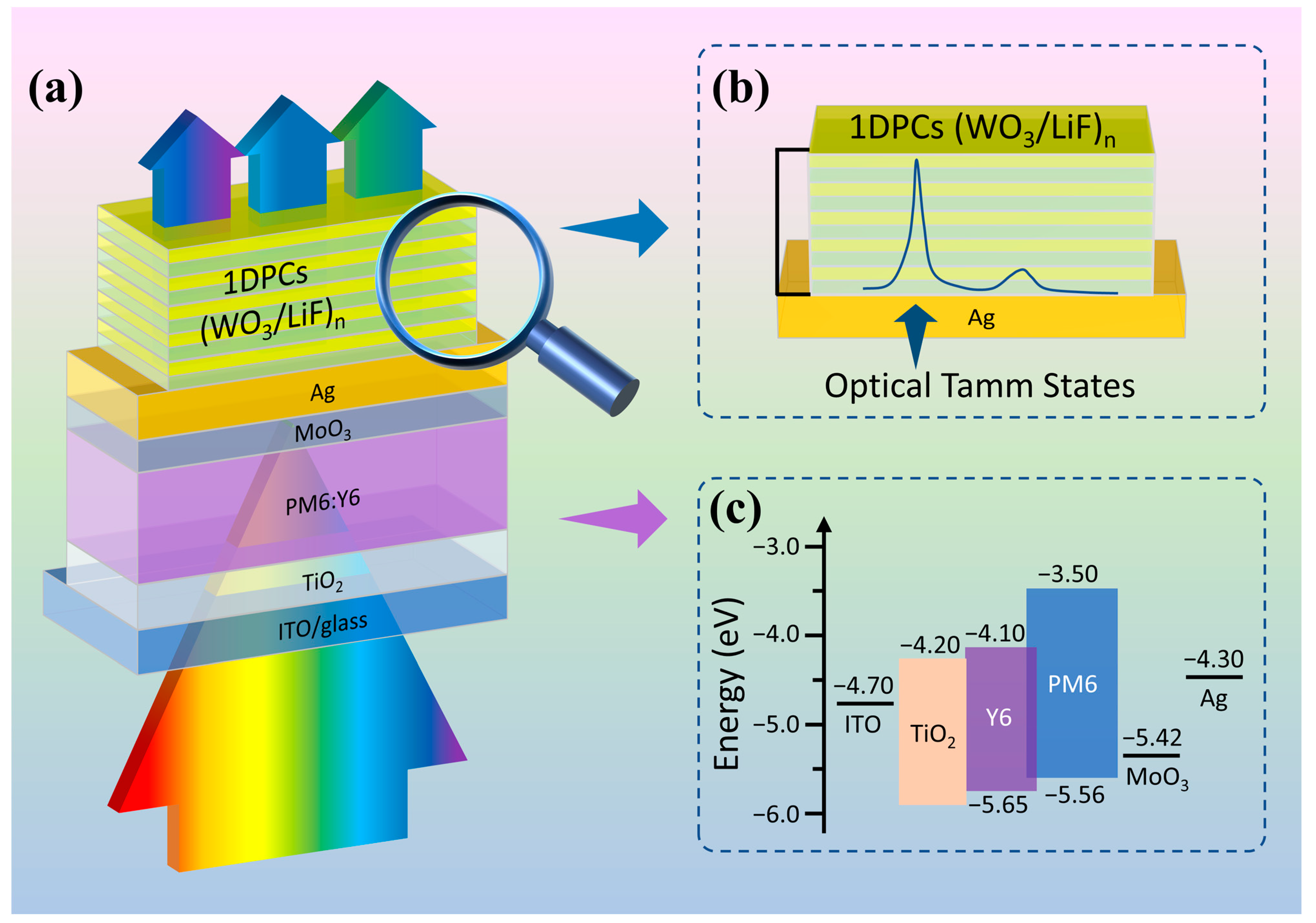
2.1. Device Structure and Materials

As illustrated in Figure 1a, the ST-OSC with an Ag/1DPC structure is configured as follows: glass/ITO/TiO2/PM6:Y6/MoO3/Ag/1DPCs. In this structure, glass/ITO (Indium Tin Oxide) is used as a transparent electrode. The TiO2 (Titanium Dioxide) is used as the electron transport layer. The PM6:Y6 represents the active layer. The copolymer PM6 acts as the donor. The non-fullerene material Y6 acts as the acceptor, whose full name is 2,2′-((2Z,2′Z)-((12,13-bis(2-ethylhexyl)-3,9-diundecyl-12,13-dihydro-[1,2,5]thiadiazolo [3,4-e]thieno [2,”3′‘:4′,5′]thieno [2′,3′:4,5]pyrrolo [3,2-g]thieno [2′,3′:4,5]thieno [3,2-b]indole-2,10-diyl)bis(me-thanylylidene))bis(5,6-difluoro-3-oxo-2,3-dihydro-1H-indene-2,1-diylidene))dimalonitrile. The MoO3 (molybdenum trioxide) is used as the hole transport layer. The silver (Ag) is used as the semitransparent electrode. Specifically, the 1DPCs depicted in Figure 1b are composed of five pairs of WO3/LiF. The thicknesses of the ITO, TiO2, PM6:Y6, and MoO3 layers are 100, 10, 80, and 10 nm, respectively. In the numerical analysis, the parameters of the Ag layer thickness, central wavelength of the 1DPCs, thickness of the first WO3 layer of the 1DPCs, and pair number of the 1DPCs will be set within a certain range, and the specified parameters will be presented in Section 3 to identify the optimal results and to elucidate the performance optimization regulation of the devices. Furthermore, Figure 1c exhibits the energy level alignment of the ST-OSCs, which was used in the theoretical simulation [47,48].

2.2. Optical Modeling Methods for ST-OSC Devices

To evaluate the performance of the ST-OSCs with an Ag/1DPC structure, optical modeling method based on the TMM is used to calculate the light absorption and transmission of the devices [16]. In brief, the optical electric field within the device is firstly calculated according to the provided schematic diagram, which is then used to calculate the monochromatic pointwise energy dissipation per unit area. The formula is given as follows [49]:
Q x = 2 π c ε 0 k n E x 2 λ
In Equation (1), c represents the speed of light, ε 0 denotes the vacuum permittivity, k signifies the extinction coefficient, and n represents the refraction index. E(x) is the total electrical optical field at x. In the calculation, the refractive index of all the layers in the devices are taken from reference [16]. The light absorption in the active layer can also be calculated as in [49].
A λ = 1 I λ x layer Q x d x
where I λ represents the light intensity in the glass transferred to the glass/ITO interface. Accordingly, the short current density (Jsc) of the device is calculated as [49]
J s c = A λ I λ h c λ q d λ
where h represents the Planck constant and q is the electron charge by assuming that the device is illuminated by AM1.5 with 100 mW/cm2 and that all the absorbed photons in the active layer can be collected by the electrode. The device is set to work stably without performance attenuation. With Jsc as input values, PCE is calculated as
P C E = V O C × J S C × F F P in × 100 %
where Voc represents the open-circuit voltage, FF denotes the fill factor, and Pin represents the input power, by setting the open voltage and fill factor of the device as empirical values of 0.83 V and 0.768, which are obtained from experimental data in the reported literature [31]. Based on the light transmission spectra of the device, the color and transparency of the ST-OSCs can be investigated by calculating the color coordinates (x, y) [16]. The PCE loss rate can be calculated using the following formula [17]:
P C E   L o s s   R a t e = P C E o p a q u e   O S C s P C E S T O S C s P C E o p a q u e   O S C s × 100 %

3. Results and Discussion

3.1. The Optical Properties of the 1DPCs and Ag/1DPC Structure

Firstly, the impact of the central wavelength of the 1DPCs on the transmittance characteristics was investigated. For this purpose, WO3 and LiF were selected as the constituent materials for the 1DPCs, where the refractive index of WO3 is 2.2 and that of LiF is 1.4. The WO3 and LiF layers were periodically stacked to form WO3/LiF multilayers. A series of 1DPCs were designed, with the central wavelength set as 450 nm, 500 nm, 550 nm, 600 nm, and 650 nm. As illustrated in Figure 2a, the results revealed that the bandwidth of the 1DPCs broadened as the central wavelength increased, leading to a corresponding redshift of the band-edge position. However, the narrow bandgap and wide passband of the 1DPCs limit their potential to enhance the PCE and modulate the color of ST-OSCs. Subsequently, in order to further enhance the performance, a 40 nm thick Ag layer was integrated on the bottom of the 1DPCs to construct an Ag/1DPC structure. As illustrated in Figure 2b, the Ag/1DPCs with central wavelengths from 450 to 650 nm can effectively narrow the transmittance passbands of the original 1DPCs, while simultaneously introducing a transmittance peak within the bandgap, with a peak transmittance exceeding 60%. This phenomenon can be attributed to the excitation of the OTSs at the Ag/1DPCs interface, resulting in a sharp transmittance peak. As the central wavelength increases from 450 to 650 nm, the transmittance peaks are accordingly redshifted from 520 to 723 nm. These results demonstrate that by adjusting the central wavelength of the Ag/1DPCs, the OTSs can be controlled to modulate the transmittance peak, thereby offering a way to regulate the color of ST-OSCs.
To further analyze the optical properties of the Ag/1DPCs, Figure 2c,d show the spatial profile of the electromagnetic field energy inside the 1DPCs and Ag/1DPCs at wavelengths ranging from 380 to 900 nm. The central wavelength was set to 550 nm. For the 1DPCs, it is observed that the electric field exhibits a greater contribution at wavelengths of both 450 nm and 700 nm. This phenomenon can be attributed to the localized electric field enhancement at the bandgap edge position, where the light is periodically modulated by the 1DPCs. For the Ag/1DPCs, the maximum electric field is observed at the interface between the two materials at a wavelength of 618 nm. The electric field energy is localized at 618 nm within the Ag/1DPCs, and it is relatively weak in the other wavelength range. This phenomenon is typical for the excitation of the OTSs. Accordingly, as illustrated in Figure 2b, a transmittance peak can be found at the wavelength of 618 nm. This demonstrates that the Ag/1DPC structure favors the reflection of more photons, thereby producing a sharp transmittance peak and resulting in enhanced monochromaticity in comparison to 1DPCs.

3.2. Comparison of the Performance of ST-OSCs with/Without Ag/1DPC Structure

To explore the performance optimization, two device structures were investigated. The reference structure is designated as glass/ITO/TiO2/PM6:Y6/MoO3/Ag. The optimized structure is similar to the reference structure, but it incorporates 1DPCs on top of the Ag layer (glass/ITO/TiO2/PM6:Y6/MoO3/Ag/1DPCs). The thicknesses of the Ag layer are set at 10 nm and 40 nm, respectively. The central wavelengths of the 1DPCs are set at 450 nm, 500 nm, 550 nm, 600 nm, and 650 nm.
In order to investigate the performance evolution of the ST-OSCs with Ag/1DPCs, the transmittance and absorption spectra of the devices were calculated using the transmission matrix method. When the thickness of the Ag layer is 10 nm and the central wavelength of 1DPCs is 450 nm, the transmittance of ST-OSCs in the range of 400 nm–500 nm is markedly low (Figure 3a). This is mainly due to the fact that the reflectivity of the optical bandgap is very high, which prevents most of the incident light from passing through and thus allows them to be reflected back into the device for reabsorption. This process eventually enhances the light absorption. Consequently, absorption peak begins to appear in the bandgap range (Figure 3d). As the central wavelength increases, the optical bandgap gradually redshifts. As a result, the range of both high reflection and enhanced absorption is accordingly redshifted. When the central wavelength is 450 nm, the device exhibits a Jsc of 17.68 mA/cm2 and a PCE of 11.2%. As the central wavelength is increased to 650 nm, the Jsc and PCE are enhanced to 18.74 mA/cm2 and 11.95%, respectively. In comparison, the Jsc and PCE of the reference device are 18.60 mA/cm2 and 11.86%. It is evident that the difference in Jsc and PCE resulting from the Ag (10 nm)/1DPCs and the reference structure is not statistically significant. When the thickness of the Ag layer is 40 nm and the central wavelength of the 1DPCs is 450 nm, the ST-OSCs exhibits a higher transmittance peak, located at 519 nm with a peak size of 38.8% (Figure 3b), than those of the reference structure (Figure 3c,f). The absorption dip is accordingly located at 519 nm (Figure 3e). Moreover, the corresponding device exhibits a Jsc of 23.43 mA/cm2 and a PCE of 14.93%. When the central wavelength is increased from 450 nm to 650 nm, the transmittance peaks present a redshift from 519 nm to 722 nm (Figure 3b), accompanied by the corresponding redshift in absorption dips (Figure 3e). As indicated in Table 1, the Jsc and PCE of the five ST-OSCs with Ag (40 nm)/1DPCs are all beyond 23.4 mA/cm2 and 14.9%. These findings demonstrate that the incorporation of the Ag/1DPCs can effectively enhance the transmittance peak intensity of the ST-OSCs and minimize their PCE loss.
To further clarify the impact of OTSs on the device performance, the optical electric field distributions of the ST-OSCs with Ag/1DPCs are investigated. As shown in Figure 4a–e, the enhanced field is localized at the Ag/1DPCs interface, exhibiting a relative field intensity enhancement of over 15 times. In contrast, the optical electric field outside the interfaces does not exhibit a notable enhancement. Furthermore, the localized field results in transmission peaks and absorption dips. These observations are attributed to the formation of OTSs by satisfying the phase-matching conditions during the reflection and transmission of incident light at the Ag/1DPCs interface. On the other hand, the maximum of the optical electric field exhibits a redshift as the central wavelength of the 1DPCs increases. This is primarily due to the fact that the excitation condition of the OTSs is strongly influenced by the change in central wavelength. In other words, the light reflection coefficient and phase will change accordingly as the central wavelength increases, resulting in the redshift of the OTSs, thus indicating the redshift of transmittance peaks and absorption dips. The color coordinates of the ST-OSCs with Ag/1DPCs were calculated based on the transmission spectra. The results are summarized in Table 2. As illustrated in Figure 4f, the colors of the ST-OSCs with Ag (10 nm)/1DPCs are yellow-green, red, and blue when the central wavelengths are 400 nm, 500 nm, and 600 nm, respectively. Meanwhile, as illustrated in Figure 4g, the colors of the ST-OSCs with Ag (40 nm)/1DPCs are light blue, yellow, and green when the central wavelengths are 400 nm, 500 nm, and 600 nm. These findings demonstrate that the devices comprising Ag (40 nm)/1DPC structures exhibit enhanced color purity, which is attributable to the narrowness of their transmission peaks. Moreover, as displayed in the color coordinate plots, the Ag (40 nm)/1DPC devices exhibit a more extensive range of selectable transmission colors by modulating the central wavelengths of the 1DPCs.

3.3. Effect of Ag Electrode Thickness on Device Performance

In this experiment, to investigate the impact of the parameters of the Ag layer thickness on the device performance, the central wavelength of the 1DPCs is set to 600 nm, and the thickness of the Ag layer is varied from 0 to 80 nm. The experiment results are summarized in Table 3.
Regarding the optical properties, it can be observed that as the thickness of the Ag layer increases from 10 nm to 30 nm (Figure 5a), the intensity of the transmittance peak reaches a maximum value of 34.8% (Figure 5f). However, upon a further increase in the thickness of the Ag layer, the intensity of the transmittance peak diminishes to 3% (Figure 5b). Figure 5d,e demonstrate that the positions of the absorption dips are aligned with those of the transmission peaks. This is due to the intensification of the OTSs with the increasing Ag layer thickness, which initially leads to an enhancement of the transmittance peak and a corresponding decrease in the absorption dip. Moreover, when the thickness of the Ag layer exceeds 30 nm, the effect of light reflection becomes the dominant factor, superseding that of the OTSs in enhancing transmittance. In addition, when the thickness of the Ag layer is increased from 20 nm to 80 nm, the wavelength of the transmittance peak exhibits a slight blueshift from 681 nm to 668 nm. This can be attributed to the fact that the increase in the thickness of the Ag layer alters the reflection coefficient and phase, which in turn affects the excitation conditions of the OTSs, thus resulting in the blueshift of the transmittance peak. In addition, with regard to the electrical properties, both Jsc and PCE exhibit an increase, ultimately converging on the performance of the opaque device, while the Ag layer thickness increases from 0 nm to 80 nm. Among them, the Jsc increased from 15.50 mA/cm2 to 24.22 mA/cm2, while the PCE increased from 9.88% to 15.44% (Figure 5c). The color of the ST-OSCs changed from blue to purple as the Ag layer thickness increased. The color coordinates of the ST-OSCs are presented in Figure 5g. Furthermore, at a transmission peak intensity of 34.8%, the corresponding Ag layer thickness is 30 nm, Jsc is 22.64 mA/cm2, and the PCE reaches 14.43%. Thus, the PCE loss is merely 6.7%. At a Ag layer thickness of 40 nm, the transmission peak intensity is 34.0%, and the PCE is 14.93%. Consequently, the PCE loss is further reduced to 3.5%.
In conclusion, the results demonstrate that the optimized parameter of the Ag layer thickness is between 30 and 40 nm. In this configuration, the transmission peak intensities of ST-OSCs can exceed 34.0%, and the PCE losses are below 6.7%, thus achieving the simultaneous enhancement of both transparency and PCE.

3.4. The Effect of the Thickness of the First WO3 Layer of the 1DPCs

To investigate the impact of the thickness of the first WO3 layer of the 1DPCs, the Ag layer thickness is fixed to 35 nm. The central wavelength of the 1DPCs with five WO3/LiF pairs is fixed to 600 nm. As illustrated in Table 4, an increase in the thickness of the first WO3 layer from 0 to 80 nm results in a redshift of the sharp transmittance peaks corresponding to the OTSs from 501 nm to 718 nm. Furthermore, the peak intensities remain above 16.8%, with the highest value reaching 44.2% (Figure 6a,b). In accordance with this, the corresponding absorption dips also exhibit a considerable redshift, from 501 nm to 718 nm (Figure 6d,e). Except for the aforementioned transmittance peaks generated by the OTSs, three transmittance peaks are observed within the wavelength range of 400 to 500 nm, which are caused by the passbands of the 1DPCs. In fact, the increase in the thickness of the first WO3 layer primarily influences the reflection phase shift in the bandgap of the 1DPCs, which in turn affects the excitation conditions of the OTSs, thus leading to the redshift of the transmittance peaks and the absorption dips. As illustrated in Figure 6c, the PCE remains within the range of 14.72% to 14.94% during the tuning of the thickness of the first WO3 layer, indicating that this parameter has a minimal impact on the PCE. As the thickness begins to increase from 0 to 10 nm, the transmittance peak intensity reaches a maximum value of 44.2%. As the thickness continues to increase to 50 nm, the peak intensity then decreases to 14.0%. Following that, when the thickness is increased to 70 nm, the peak intensity rises to 37.4%. Finally, when the thickness reaches 90 nm, the peak intensity decreases to 27.0%. It is evident that a local maximum value of the intensity of the transmittance peak will periodically emerge. Moreover, the color of the ST-OSCs with the increasing thickness of the first WO3 layer is observed to be blue, light blue, purple, and blue. The color coordinates of the ST-OSCs are presented in Figure 5h and Table 4. Therefore, to guarantee the high transparency of the device, it is essential to carefully select the thickness of the first WO3 layer, such as 10 or 70 nm, which corresponds to the local maximum values of the peak intensity.

3.5. The Effect of the Pair Number of WO3/LiF in 1DPCs

To study the impact of the pair number of WO3/LiF in 1DPCs, some structural parameters are established as follows: The Ag layer thickness is maintained at 35 nm. The central wavelength of the 1DPCs is fixed at 600 nm. And the pair number of WO3/LiF is set to vary from 0 to 9. With regard to optical properties, notable transmittance peaks and absorption dips can be observed when the number of (WO3/LiF) pairs is increased from 0 to 9. The wavelength of the transmittance peak exhibits a redshift from 670 nm to a maximum value of 690 nm, followed by a blueshift to 669 nm (Figure 7a,b). At a wavelength of 690 nm, the corresponding WO3/LiF is three pairs (Figure 7f). Meanwhile, the intensity of the transmittance peak exhibits an enhancement from 5% to a maximum of 38.8%, after which it declines to 10.6%. At the maximum peak intensity of 38.8%, the corresponding WO3/LiF is five pairs (Figure 7f). Moreover, the full width at half maximum (FWHM) of the transmittance peaks and absorption dips decrease with the increase in the pair number of WO3/LiF, thereby producing a narrower profile for transmittance peaks and absorption dips (Figure 7d,e). These findings will be beneficial in optimizing the transparency and monochromaticity. In addition, with regard to the electrical properties, the Jsc and PCE of these devices are maintained within the range of 14.57% to 14.94% (Figure 7c). It can be calculated that the PCE losses induced by the increase in the pair number of WO3/LiF are below 6%. Additionally, the color coordinates of the devices are summarized in Table 5 and Figure 5i. It indicates that the see-through color of the device can be tuned from light blue to violet and then to blue. Consequently, these findings indicate that tuning the pair number of WO3/LiF does not negatively impact the PCE performance but allows for the achievement of colorful ST-OSCs with high transparency and high efficiency.

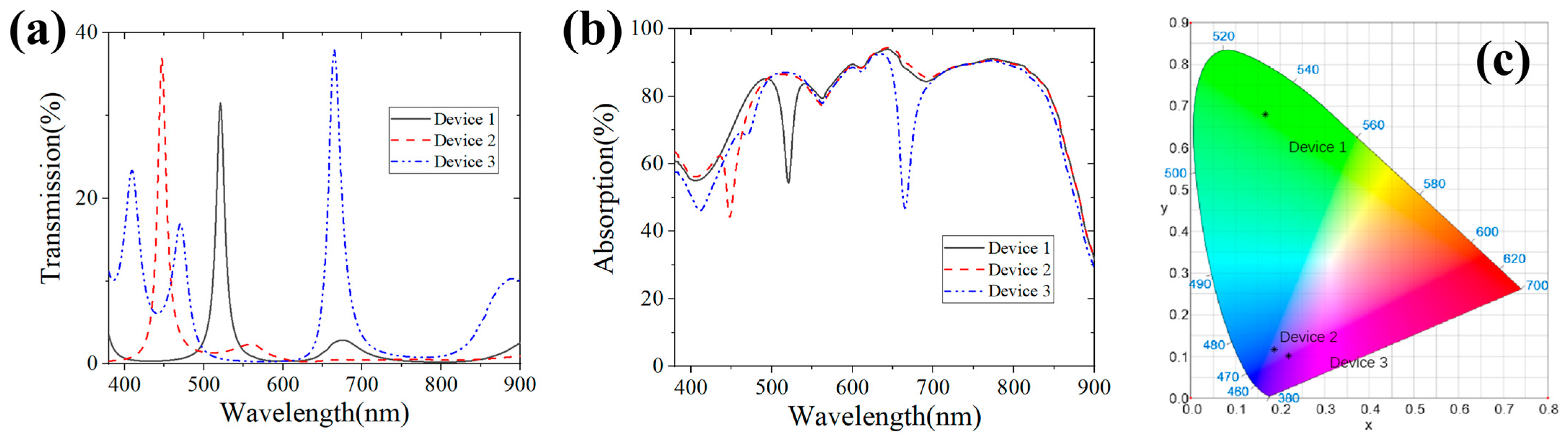
3.6. Devices with Optimized Structural Parameters

To obtain colorful ST-OSCs with the desired characteristics, the optimal parameters for the thickness of the Ag layer, the thickness of the first WO3 layer, and the central wavelength were identified. In this part, the objective of the optimization is to design devices with transmittance peaks exceeding 30% and PCE losses below 5.5%. The simulation results successfully yielded three classes of devices exhibiting different colors: green, blue, and purple. Firstly, device 1 exhibits a wavelength of the transmittance peak of 521 nm, which corresponds to a green coloration with a peak intensity of 31.5% (Figure 8a,b). Meanwhile, the Jsc and PCE are 23.84 mA/cm2 and 15.20%. Secondly, device 2 displays a blue transmittance color. The transmittance peak is located at 447 nm, with a peak intensity of 37.0%. The Jsc and PCE are 23.90 mA/cm2 and 15.24%. Furthermore, device 3 exhibits a purple transmittance color. The transmittance peak is accordingly located at 665 nm, with a peak intensity of 37.9%. The Jsc and PCE are 23.02 mA/cm2 and 14.67%. The performance parameters of the devices and the corresponding optimal parameters are also summarized in Table 6. The results indicate that the PCE losses are below 3%, with a minimum value of 1%, and that the intensities of the transmittance peak are beyond 30%, with a maximum value of 37.9%. According to these results, the trade-off between transparency and PCE can be estimated by comparing the values of Tmax (peak intensity) and PCE loss. As illustrated in Table 3, the thickness of the Ag layer has a large impact on both the Tmax and PCE loss. The maximum intensity (Tmax) is observed to reach a value of 34.0 to 34.8%, while the PCE loss is found to be 3.5 to 6.7%. This result shows the exchange level between the number of transmitted photons and their resulting PCE losses. Furthermore, as illustrated in Table 4, the thickness of the first WO3 layer exhibits the main impact on see-through colors. The aforementioned ST-OSCs display a Tmax range of 14.0 to 44.2%, accompanied by a PCE loss range of 3.4 to 4.8%. This result suggests that the conversion factors between the Tmax and PCE loss at different wavelengths are not fixed constants. The numerical solution to this relationship can be obtained by simulation. It can be observed that a relatively minor PCE loss is accompanied by a higher Tmax in the blue-light region. Moreover, as illustrated in Table 5, the simulation results for the pair number of WO3/LiF indicate that the maximum Tmax is 38.8% and the corresponding PCE loss is 5.0% when the position of the transmittance peak is located at 673 nm in the red-light region. The simulation results also indicate that the absorption of the active layer is between 50 and 80% in the visible range of 400 to 530 nm. Therefore, devices with transmittance peaks in this range are susceptible to elevated transmission peak intensities and minimal PCE loss. Furthermore, the absorption of the active layer is almost above 80% in the visible range of 530 to 700 nm. In this range, the device exhibits a higher PCE loss, as more photons that would be absorbed are transmitted to the outside of the device via the OTSs. Ultimately, these findings provide compelling evidence that the colorful ST-OSCs, including green, blue, and purple (Figure 8c), can be achieved with both a high transparency over 30% and a high efficiency (PCE loss below 5.5%) by enhancing the performance based on the Ag/1DPCs optical structure. The key performance parameters of some comparable ST-OSCs with/without optical structures is summarized in Table 7.

4. Conclusions

This study conducted a comparative analysis of the optical attributes of a 1DPC structure in conjunction with an Ag layer, revealing the presence of OTSs at the Ag/1DPCs interface. These OTSs are instrumental in generating a distinct transmittance peak. By tuning the central wavelength of 1DPCs, it is possible to alter the spectral characteristics and the intensity of their transmittance peaks. This modulation affords precise control over the light absorption, transmittance, and color of ST-OSCs. Furthermore, the potential for optimizing the performance of ST-OSCs was investigated with regard to the OTSs in Ag/1DPCs. Key parameters included the thickness of the Ag layer, the central wavelength of 1DPCs, the thickness of the first WO3 layer, and the pair number of WO3/LiF. When the Ag layer thickness was 30 nm, the color of the ST-OSC is blue, with a maximum peak intensity of 34.8% and a PCE of 14.43%. Notably, deviations from this thickness threshold result in diminished device transparency. In addition, variations in the thickness of the first WO3 layer and the pair number of WO3/LiF were discovered to have a significant impact on the wavelength and intensity of the transmittance peak, the PCE, and the color of the ST-OSCs. An optimum thickness of 10 nm for the first WO3 layer yielded a peak intensity of 44.2%. As this thickness increased, the color of ST-OSCs gradually shifted from blue to light blue, then to purple, and finally back to blue. Similarly, the pair number of WO3/LiF was identified as a pivotal determinant of color, with an arrangement of five pairs optimizing the peak intensity to 38.8%. As the pair number of WO3/LiF increased, the color of the ST-OSCs also altered from light blue to white-purple, then from white-purple to purple, and finally returning to blue. Ultimately, after further optimization of the structural parameters, three ST-OSC prototypes were successfully designed, achieving PCEs beyond 14.6%, transmittance peak intensities exceeding 30%, and transmittance colors including green, blue, and violet. This research provides an innovative design of colorful ST-OSCs with both high transparency and high efficiency.

Author Contributions

J.Z. (Junwei Zhao): Conceptualization, Software, Investigation, Data curation, and Writing—original draft. S.L.: Validation and Visualization. J.Z. (Jinxin Zhou): Data curation and Formal analysis. F.G.: Software and Data curation. J.L.: Writing—review and editing. Y.L.: Methodology, Supervision, Funding acquisition, and Writing—review and editing. H.X.: Conceptualization, Funding acquisition, Supervision, Validation, and Writing—review and editing. All authors have read and agreed to the published version of the manuscript.

Funding

This research was supported by the National Natural Science Foundation of China (12174120, 11774099), The 111 Project (D18019), Leading talents of Guangdong province program (2016LJ06G689), and Laboratory of Lingnan Modern Agriculture Project (NT2021009).

Data Availability Statement

The data for this paper are not publicly available because they are part of ongoing work.

Conflicts of Interest

The authors declare no conflict of interest.

References

  1. Bailey-Salzman, R.F.; Rand, B.P.; Forrest, S.R. Semitransparent organic photovoltaic cells. Appl. Phys. Lett. 2006, 88, 3693. [Google Scholar] [CrossRef]
  2. Traverse, C.J.; Pandey, R.; Barr, M.C.; Lunt, R.R. Emergence of highly transparent photovoltaics for distributed applications. Nat. Energy 2017, 2, 849–860. [Google Scholar] [CrossRef]
  3. Liu, Z.X.; Yu, Z.P.; Shen, Z.; He, C.; Lau, T.K.; Chen, Z.; Zhu, H.; Lu, X.; Xie, Z.; Chen, H.; et al. Molecular insights of exceptionally photostable electron acceptors for organic photovoltaics. Nat. Commun. 2021, 12, 3049. [Google Scholar] [CrossRef]
  4. Zhou, G.; Zhang, M.; Xu, J.; Yang, Y.; Hao, T.; Zhu, L.; Zhou, L.; Zhu, H.; Zou, Y.; Wei, G.; et al. Spontaneous carrier generation and low recombination in high-efficiency non-fullerene solar cells. Energ. Env. Sci. 2022, 15, 3483–3493. [Google Scholar] [CrossRef]
  5. Xu, T.; Deng, B.; Zheng, K.; Li, H.; Wang, Z.; Zhong, Y.; Zhang, C.; Leveque, G.; Grandidier, B.; Bachelot, R.; et al. Boosting the Performances of Semitransparent Organic Photovoltaics via Synergetic Near-Infrared Light Management. Adv. Mater. 2024, 36, 2311305. [Google Scholar] [CrossRef]
  6. Deng, B.; Zheng, K.; Wang, Z.; Yin, L.; Dong, H.; Zhang, C.; Treguer-Delapierre, M.; N’konou, K.; Grandidier, B.; Wang, S.; et al. Multifunctional Semitransparent Organic Photovoltaics with High-Throughput Screened Infrared Reflector. ACS Energy Lett. 2024, 9, 976–984. [Google Scholar] [CrossRef]
  7. Li, Y.; Wang, J.; Yan, C.; Zhang, S.; Cui, N.; Liu, Y.; Li, G.; Cheng, P. Optical and electrical losses in semitransparent organic photovoltaics. Joule 2024, 8, 527–541. [Google Scholar] [CrossRef]
  8. Kim, J.Y.; Jeon, S.J.; Lee, H.S.; Han, Y.W.; Kim, Y.C.; Yang, N.G.; Kim, G.W.; Jang, E.M.; Kim, J.H.; Moon, D.K. Distribution of dual additives enables efficient semi-transparent layer-by-layer architecture of organic solar cells. J. Mater. Chem. C Mater. Opt. Electron. Devices 2024, 12, 598–5915. [Google Scholar] [CrossRef]
  9. Zhu, L.; Zhang, M.; Xu, J.; Li, C.; Yan, J.; Zhou, G.; Zhong, W.; Hao, T.; Song, J.; Xue, X.; et al. Single-junction organic solar cells with over 19% efficiency enabled by a refined double-fibril network morphology. Nat. Mater. 2022, 21, 656–663. [Google Scholar] [CrossRef] [PubMed]
  10. Guan, S.; Li, Y.; Xu, C.; Yin, N.; Xu, C.; Wang, C.; Wang, M.; Xu, Y.; Chen, Q.; Wang, D.; et al. Self-Assembled Interlayer Enables High-Performance Organic Photovoltaics with Power Conversion Efficiency Exceeding 20%. Adv. Mater. 2024, 36, 2400342. [Google Scholar] [CrossRef] [PubMed]
  11. Kini, G.P.; Jeon, S.J.; Moon, D.K. Latest Progress on Photoabsorbent Materials for Multifunctional Semitransparent Organic Solar Cells. Adv. Funct. Mater. 2021, 31, 2007931. [Google Scholar] [CrossRef]
  12. Fukuda, K.; Yu, K.; Someya, T. The Future of Flexible Organic Solar Cells. Adv. Energy Mater. 2020, 10, 2000765. [Google Scholar] [CrossRef]
  13. Ma, L.; Cui, Y.; Zhang, J.; Xian, K.; Chen, Z.; Zhou, K.; Zhang, T.; Wang, W.; Yao, H.; Zhang, S.; et al. High-Efficiency and Mechanically Robust All-Polymer Organic Photovoltaic Cells Enabled by Optimized Fibril Network Morphology. Adv. Mater. 2023, 35, 2208926. [Google Scholar] [CrossRef] [PubMed]
  14. Safat Dipta, S.; Schoenlaub, J.; Habibur Rahaman, M.; Uddin, A. Estimating the potential for semitransparent organic solar cells in agrophotovoltaic greenhouses. Appl. Energy 2022, 328, 120208. [Google Scholar] [CrossRef]
  15. Xiao, L.; Zhang, H.; Li, S.; Cheng, Q.; Zhang, Y.; Li, Y.; Zhang, Y.; Zhou, H. The Role of Device Architecture and Interfacial Layer on Performance of Semitransparent Organic Solar Cells. Sol. RRL 2024, 8, 2400126. [Google Scholar] [CrossRef]
  16. Zhong, J.; Liang, W.; Long, Y. Simultaneously improving efficiency and transparency of semitransparent organic solar cells by constructing semitransparent microcavity. Optik 2018, 171, 706–714. [Google Scholar] [CrossRef]
  17. Zhong, J.; Xu, H.; Zhao, J.; Gao, F.; Zhou, J.; Long, Y. Magnesium fluoride microcavity-based non-fullerene semitransparent organic solar cells with high peak transmittance and low efficiency loss rate. Org. Electron. 2023, 121, 106864. [Google Scholar] [CrossRef]
  18. Gao, N.; Bin, H.; Wu, S.; Janssen, R.A.J.; Li, Y. Semitransparent organic solar cells with high light utilization efficiency and color rendering index. Sci. China Chem. 2024, 67, 2248–2256. [Google Scholar] [CrossRef]
  19. Liu, X.; Liu, X.; Xia, Z.; Ji, Y.; Zhang, D.; Cheng, Y.; Liu, X.; Yuan, J.; Yang, X.; Huang, W. A semitransparent organic solar cell with a bifacial factor of 99.1%. Mater. Today Energy 2024, 44, 101614. [Google Scholar] [CrossRef]
  20. Zhao, M.; Wu, J.; Tang, H.; Yi, X.; Liu, Z.; Huang, M.; Fu, Y.; Xie, Z. A Novel Ultra-Thin and Smooth Sm:Ag Composite Electrode with High Visible Transmittance Enables Efficient Color-Neutral Semitransparent Organic Solar Cells. Adv. Opt. Mater. 2024, 2401776. [Google Scholar] [CrossRef]
  21. Duan, L.; Hoex, B.; Uddin, A. Progress in Semitransparent Organic Solar Cells. Sol. RRL 2021, 5, 2100041. [Google Scholar] [CrossRef]
  22. Kumar, P.; You, S.; Vomiero, A. Recent Progress in Materials and Device Design for Semitransparent Photovoltaic Technologies. Adv. Energy Mater. 2023, 13, 2301555. [Google Scholar] [CrossRef]
  23. Han, G.; Yi, Y.; Shuai, Z. From Molecular Packing Structures to Electronic Processes: Theoretical Simulations for Organic Solar Cells. Adv. Energy Mater. 2018, 8, 201702743. [Google Scholar] [CrossRef]
  24. Su, W.; Fan, Q.; Guo, X.; Wu, J.; Zhang, M.; Li, Y. Efficient as-cast semi-transparent organic solar cells with efficiency over 9% and a high average visible transmittance of 27.6%. Phys. Chem. Chem. Phys. 2019, 21, 10660–10666. [Google Scholar] [CrossRef]
  25. Xu, T.; Luo, Y.; Wu, S.; Deng, B.; Chen, S.; Zhong, Y.; Wang, S.; Leveque, G.; Bachelot, R.; Zhu, F. High-Performance Semitransparent Organic Solar Cells: From Competing Indexes of Transparency and Efficiency Perspectives. Adv. Sci. 2022, 9, 2202150. [Google Scholar] [CrossRef]
  26. Hu, Z.; Wang, J.; Ma, X.; Gao, J.; Xu, C.; Yang, K.; Wang, Z.; Zhang, J.; Zhang, F. A critical review on semitransparent organic solar cells. Nano Energy 2020, 78, 105376. [Google Scholar] [CrossRef]
  27. Zhang, Y.F.; Chen, W.S.; Chen, J.D.; Ren, H.; Hou, H.Y.; Tian, S.; Ge, H.R.; Ling, H.H.; Zhang, J.L.; Mao, H.; et al. Optically Enhanced Semitransparent Organic Solar Cells with Light Utilization Efficiency Surpassing 5.5%. Adv. Energy Mater. 2024, 14, 202400970. [Google Scholar] [CrossRef]
  28. Zhao, L.; Huang, X.; Wang, Y.; Young Jeong, S.; Huang, B.; Deng, J.; Liu, J.; Cheng, Y.; Young Woo, H.; Wu, F.; et al. Combination of highly photovoltaic and highly transparent materials enables record performance semitransparent organic solar cells. Chem. Eng. J. 2023, 451, 139081. [Google Scholar] [CrossRef]
  29. Xu, T.; Deng, B.; Zhao, Y.; Wang, Z.; Lévêque, G.; Lambert, Y.; Grandidier, B.; Wang, S.; Zhu, F. High-Throughput Computing Guided Low/High Index Optical Coupling Layer for Record-Performance Semitransparent Organic Solar Cells. Adv. Energy Mater. 2023, 13, 202301367. [Google Scholar] [CrossRef]
  30. Hu, Z.; Wang, Z.; An, Q.; Zhang, F. Semitransparent polymer solar cells with 12.37% efficiency and 18.6% average visible transmittance. Sci. Bull. 2020, 65, 131–137. [Google Scholar] [CrossRef]
  31. Yuan, J.; Zhang, Y.; Zhou, L.; Zhang, G.; Yip, H.; Lau, T.; Lu, X.; Zhu, C.; Peng, H.; Johnson, P.A.; et al. Single-Junction Organic Solar Cell with over 15% Efficiency Using Fused-Ring Acceptor with Electron-Deficient Core. Joule 2019, 3, 1140–1151. [Google Scholar] [CrossRef]
  32. Rasool, S.; Yeop, J.; Cho, H.W.; Lee, W.; Kim, J.W.; Yuk, D.; Kim, J.Y. Path to the fabrication of efficient, stable and commercially viable large-area organic solar cells. Mater. Futures 2023, 2, 32102. [Google Scholar] [CrossRef]
  33. Li, M.; An, T.; Ou, Z.; Jin, K.; Jin, Z.; Yan, K.; Tian, H.; Wang, W.; Yang, S.; Wang, G.; et al. A tetracyclic-bislactone-based copolymer donor for efficient semitransparent organic photovoltaics. Mater. Adv. 2023, 4, 2991–2998. [Google Scholar] [CrossRef]
  34. Hong, E.; Li, Z.; Zhang, X.; Fan, X.; Fang, X. Deterministic Fabrication and Quantum-Well Modulation of Phase-Pure 2D Perovskite Heterostructures for Encrypted Light Communication. Adv. Mater. 2024, 36, e2400365. [Google Scholar] [CrossRef] [PubMed]
  35. Liu, D.; Yin, Y.; Liu, F.; Miao, C.; Zhuang, X.; Pang, Z.; Xu, M.; Chen, M.; Yang, Z. Thickness-dependent highly sensitive photodetection behavior of lead-free all-inorganic CsSnBr3 nanoplates. Rare Met. 2022, 41, 1753–1760. [Google Scholar] [CrossRef]
  36. Zhong, J.; Xiao, Z.; Liang, W.; Wu, Y.; Ye, Q.; Xu, H.; Deng, H.; Shen, L.; Feng, X.; Long, Y. Highly Efficient and High Peak Transmittance Colorful Semitransparent Organic Solar Cells with Hybrid-Electrode-Mirror Microcavity Structure. Acs Appl. Mater. Inter. 2019, 11, 47992–48001. [Google Scholar] [CrossRef]
  37. Li, X.; Xia, R.; Yan, K.; Ren, J.; Yip, H.; Li, C.; Chen, H. Semitransparent Organic Solar Cells with Vivid Colors. Acs Energy Lett. 2020, 5, 3115–3123. [Google Scholar] [CrossRef]
  38. Yeom, H.R.; Song, S.; Park, S.Y.; Ryu, H.S.; Kim, J.W.; Heo, J.; Cho, H.W.; Walker, B.; Ko, S.; Woo, H.Y.; et al. Aesthetic and colorful: Dichroic polymer solar cells using high-performance Fabry-Pérot etalon electrodes with a unique Sb2O3 cavity. Nano Energy 2020, 77, 105146. [Google Scholar] [CrossRef]
  39. Han, D.; Han, S.; Bu, Z.; Deng, Y.; Liu, C.; Guo, W. Flexible Color Tunability and High Transmittance Semitransparent Organic Solar Cells. Sol. RRL 2022, 6, 202200441. [Google Scholar] [CrossRef]
  40. Cetinkaya, C.; Cokduygulular, E.; Kinaci, B.; Emik, S.; Sonmez, N.A.; Ozcelik, S. Enhancement of color and photovoltaic performance of semi-transparent organic solar cell via fine-tuned 1D photonic crystal. Sci. Rep. 2022, 12, 19400. [Google Scholar] [CrossRef]
  41. Yu, W.; Shen, L.; Shen, P.; Long, Y.; Sun, H.; Chen, W.; Ruan, S. Semitransparent Polymer Solar Cells with 5% Power Conversion Efficiency Using Photonic Crystal Reflector. ACS Appl. Mater. Inter. 2014, 6, 599–605. [Google Scholar] [CrossRef] [PubMed]
  42. Zhang, D.; Jiang, X.; Wang, R.; Xie, H.; Ma, G.; Ou, Q.; Chen, Y.; Li, Y.; Tang, J. Enhanced Performance of Semitransparent Inverted Organic Photovoltaic Devices via a High Reflector Structure. ACS Appl. Mater. Inter. 2013, 5, 10185–10190. [Google Scholar] [CrossRef] [PubMed]
  43. Yu, W.; Shen, L.; Jia, X.; Liu, Y.; Guo, W.; Ruan, S. Improved color rendering index of low band gap semi-transparent polymer solar cells using one-dimensional photonic crystals. Rsc Adv. 2015, 5, 54638–54644. [Google Scholar] [CrossRef]
  44. Gao, H.; Li, P.; Yang, S. Tunable multichannel optical absorber based on coupling effects of optical Tamm states in metal-photonic crystal heterostructure-metal structure. Opt. Commun. 2020, 457, 124688. [Google Scholar] [CrossRef]
  45. Elsayed, H.A.; Taha, T.A.; Algarni, S.A.; Ahmed, A.M.; Mehaney, A. Evolution of optical Tamm states in a 1D photonic crystal comprising a nanocomposite layer for optical filtering and reflecting purposes. Opt. Quant. Electron. 2022, 54, 312. [Google Scholar] [CrossRef]
  46. Shen, P.; Yao, M.; Liu, J.; Long, Y.; Guo, W.; Shen, L. Colored semitransparent polymer solar cells with a power conversion efficiency of 9.36% achieved by controlling the optical Tamm state. J. Mater. Chem. A 2019, 7, 4102–4109. [Google Scholar] [CrossRef]
  47. Lu, S.; Guan, X.; Li, X.; Sha, W.E.I.; Xie, F.; Liu, H.; Wang, J.; Huang, F.; Choy, W.C.H. A New Interconnecting Layer of Metal Oxide/Dipole Layer/Metal Oxide for Efficient Tandem Organic Solar Cells. Adv. Energy Mater. 2015, 5, 1500631. [Google Scholar] [CrossRef]
  48. Bai, Y.; Han, F.; Tian, S.; Wang, F.; Jiang, S.; Wang, J.; Huang, T.; Tan, Z. Balance PCE, AVT and CRI for good eye comfort semi-transparent organic photovoltaics via Ga2O3 or In2O3 electron collection layers. Org. Electron. 2022, 108, 106572. [Google Scholar] [CrossRef]
  49. Long, Y. Effects of metal electrode reflection and layer thicknesses on the performance of inverted organic solar cells. Sol. Energy Mater. Sol. Cells 2010, 94, 744–749. [Google Scholar] [CrossRef]
  50. Huang, X.; Ren, X.; Cheng, Y.; Zhang, Y.; Sun, Z.; Yang, S.; Kim, S.; Yang, C.; Wu, F.; Chen, L. Collaborative regulation strategy of donor and acceptor analogues realizes multifunctional semitransparent organic solar cells with excellent comprehensive performance. Energy Environ. Sci. 2024, 17, 2825–2836. [Google Scholar] [CrossRef]
  51. Paci, B.; Righi Riva, F.; Generosi, A.; Guaragno, M.; Mangiacapre, E.; Brutti, S.; Wagner, M.; Distler, A.; Egelhaaf, H. Semitransparent Organic Photovoltaic Devices: Interface/Bulk Properties and Stability Issues. Nanomaterials 2024, 14, 269. [Google Scholar] [CrossRef] [PubMed]
  52. Liu, W.; Sun, S.; Zhou, L.; Cui, Y.; Zhang, W.; Hou, J.; Liu, F.; Xu, S.; Zhu, X. Design of Near-Infrared Nonfullerene Acceptor with Ultralow Nonradiative Voltage Loss for High-Performance Semitransparent Ternary Organic Solar Cells. Angew. Chem. Int. Ed. 2022, 61, e202116111. [Google Scholar] [CrossRef] [PubMed]
  53. Bai, Y.; Han, F.; Shi, R.; Wang, F.; Jiang, S.; Wang, J.; Tan, Z. High-Efficiency Microcavity Semitransparent Organic Photovoltaics with Simultaneously Improved Average Visible Transmittance and Color Rendering Index. Sol. RRL 2022, 6, 202200174. [Google Scholar] [CrossRef]
  54. Sung, Y.; Li, M.; Luo, D.; Li, Y.; Biring, S.; Huang, Y.; Wang, C.; Liu, S.; Wong, K. A micro-cavity forming electrode with high thermal stability for semi-transparent colorful organic photovoltaics exceeding 13% power conversion efficiency. Nano Energy 2021, 80, 105565. [Google Scholar] [CrossRef]
Figure 1. (a) A schematic diagram of the ST-OSCs with Ag/1DPC structures based on optical Tamm states. (b) A schematic diagram of optical Tamm states excited at the interface of the Ag/1DPCs. (c) An energy level diagram of the ST-OSCs using PM6:Y6 as their active layer [47,48].
Photonics 11 01030 g001
Figure 2. The simulation results for the transmittance spectra of (a) 1DPCs and (b) Ag/1DPCs. The spatial profile of the optical electric field energy inside the (c) 1DPCs and (d) Ag/1DPCs at wavelengths ranging from 380 to 900 nm.
Photonics 11 01030 g002
Figure 3. The simulation results for the transmittance spectra of the ST-OSCs with (a) Ag (10 nm)/1DPCs, (b) Ag (40 nm)/1DPCs, and (c) Ag electrodes. The simulation results for the absorption spectra of the ST-OSCs with (d) Ag (10 nm)/1DPCs, (e) Ag (40 nm)/1DPCs, and (f) Ag electrodes.
Photonics 11 01030 g003
Figure 4. The distributions of the optical electric field inside the ST-OSCs with Ag (40 nm)/1DPCs when the central wavelengths of the 1DPCs are (a) 450, (b) 500, (c) 550, (d) 600, and (e) 650 nm. The chromaticity diagram of the ST-OSCs with (f) Ag (10 nm)/1DPCs and (g) Ag (40 nm)/1DPCs. The black dots denote the color coordinates for the ST-OSC devices with the central wavelength of 1DPCs increased from 400 to 650 nm.
Photonics 11 01030 g004
Figure 5. The simulation results for the transmission spectra of the ST-OSCs with (a) Ag (0 to 40 nm)/1DPCs and (b) Ag (40 to 80 nm)/1DPCs. (c) The summarized performance of the ST-OSCs with Ag (0 to 80 nm)/1DPCs in Jsc and PCE. The simulation results for the absorption spectra of ST-OSCs with (d) Ag (0 to 40 nm)/1DPCs and (e) Ag (40 to 80 nm)/1DPCs. (f) The summarized performance of the ST-OSCs with Ag (0 to 80 nm)/1DPCs in wavelength and Tmax of transmission peaks. The chromaticity diagrams of the ST-OSCs are calculated based on the fine-tuned parameters, including (g) the Ag layer thickness, (h) the first WO3 layer thickness, and (i) the pair number of WO3/LiF.
Photonics 11 01030 g005
Figure 6. The simulation results for the transmission spectra of the ST-OSCs containing Ag/1DPCs with first WO3 layer thicknesses of (a) 0 to 40 nm and (b) 50 to 90 nm. (c) The summarized performance in Jsc and PCE of the ST-OSCs containing Ag/1DPCs with different thicknesses of the first WO3 layer. The simulation results for the absorption spectra of the ST-OSCs with first WO3 layer thicknesses of (d) 0 to 40 nm and (e) 50 to 90 nm. (f) The summarized performance of the ST-OSCs in terms of wavelengths and Tmax of transmission peaks.
Photonics 11 01030 g006
Figure 7. The simulation results for the transmission spectra of the ST-OSCs with pair numbers of WO3/LiF in their 1DPCs from (a) 0 to 4 and (b) 5 to 9. (c) The Jsc and PCE of ST-OSCs with varying pair numbers of WO3/LiF in their 1DPCs. The simulation results for the absorption spectra of the ST-OSCs with pair numbers of WO3/LiF in their 1DPCs from (d) 0 to 4 and (e) 5 to 9. (f) The summarized performance of ST-OSCs in terms of wavelength and Tmax of transmission peaks.
Photonics 11 01030 g007
Figure 8. The simulation results for the (a) transmission spectra and (b) absorption spectra of the three optimal devices and their calculated (c) chromaticity diagrams.
Photonics 11 01030 g008
Table 1. The optical and electrical performance results for the ST-OSCs with Ag (40 nm)/1DPCs.
DeviceCentral Wavelength (nm)Jsc (mA/cm2)PCE (%)PCE Loss Rate
(%)
Transmittance Peak (nm)Tmax (%)
ST-OSCs with Ag/1DPCs450 nm23.4314.933.551938.8
500 nm23.5014.963.357027.3
550 nm23.4914.973.261717.2
600 nm23.4314.933.567034.0
650 nm23.4614.953.472227.7
Control Device with 100 nm Ag electrode/24.2715.47///
Table 2. The color coordinates of the ST-OSCs with Ag (40 nm)/1DPCs.
1DPCs10 nm Ag
CIE-x
10 nm Ag
CIE-y
40 nm Ag
CIE-x
40 nm Ag
CIE-y
400 nm0.31820.48140.19840.2558
450 nm0.45000.49860.26560.6256
500 nm0.49480.32760.43400.4847
550 nm0.23980.07990.34960.1383
600 nm0.15100.09340.18730.0839
650 nm0.14680.20850.14510.1528
Table 3. The optical and electrical performance results for the ST-OSCs with Ag (0 to 80 nm)/1DPCs.
Ag (nm)Jsc (mA/cm2)PCE (%)PCE Loss Rate (%)Transmittance Peak (nm)Tmax (%)CIExCIEy
015.509.8836.1--0.14430.1069
1018.4911.7923.8--0.15100.0934
2021.1713.4912.868128.00.16160.0868
3022.6414.436.767334.80.17510.0846
4023.4314.933.567034.00.18730.0839
5023.8415.21.766824.70.19400.0825
6024.0615.340.866814.60.19490.0798
7024.1715.410.46687.00.19270.0762
8024.2215.440.26683.00.18920.0723
Table 4. The optical and electrical performance results for the ST-OSCs with different thicknesses of the first WO3 layer.
WO3 (nm)Jsc (mA/cm2)PCE (%)PCE Loss Rate (%)Transmittance Peak (nm)Tmax (%)CIExCIEy
023.4214.943.450136.90.13180.1200
1022.2314.81 4.351244.20.12850.1712
2022.1414.754.753037.40.14520.2346
3022.1414.754.755627.20.19580.2459
4023.1114.734.858516.80.24210.1826
5023.1014.724.861814.00.21910.1308
6023.0914.724.864923.00.21670.1014
7023.1014.734.867637.40.17320.0805
8023.1014.734.870035.90.15060.0699
9023.1014.724.871827.00.14480.0683
Table 5. The optical and electrical performance results for the ST-OSCs with different pair numbers of WO3/LiF.
PairsJsc (mA/cm2)PCE (%)PCE Loss Rate (%)Transmittance Peak (nm)Tmax (%)CIExCIEy
023.4314.943.4--0.20010.2183
123.0814.71 4.967050.21570.2674
222.8614.575.868610.00.28410.2918
322.9414.625.569021.30.24930.1468
423.0314.685.167933.30.21350.0920
523.0414.695.067338.80.19800.0921
623.1014.724.867135.30.18160.0842
723.1914.804.367026.90.16660.0781
823.214.804.366917.80.15490.0751
923.214.804.366910.60.14770.0754
Table 6. Photovoltaic parameters for ST-OSCs with colors of green, blue, and purple.
Ag (nm)WO3 (nm)Central Wavelength (nm)Jsc (mA/cm2)PCE (%)PCE Loss Rate (%)Transmittance Peak (nm)Tmax (%)CIExCIEy
Devic1 (green)504746523.8415.201.752131.50.20060.6767
Devic2 (blue)554038523.9015.241.544737.00.18700.1159
Devic3 (purple)356560023.0214.675.266537.90.19580.0906
Table 7. Summary of key performance results for some comparable ST-OSCs.
RefActive LayerTop ElectrodePCE (%)Tmax (%)λ@Tmax
Huang [50]PCE10-2F/Y6Ag 15 nm10.48//
Huang [50]PM6:L8-BOAg 15 nm12.88//
Paci [51]PM6:Y6AgNWs6.7//
Liu [52]PM6:Y6:SNAg 20 nm15.9//
Bai [53]PM6:Y6Ag/MoO3/Ag11.44–11.91//
Sung [54]PM6:Y6Ag/HATCN/Ag13.2815.6470
Li [37]PM6:Y6Ag/TeO2/Ag13.9531.0438
Li [37]PM6:Y6Ag/TeO2/Ag14.3021.8529
Li [37]PM6:Y6Ag/TeO2/Ag14.1025.2656
This workPM6:Y6Ag/1DPCs15.2437.0447
This workPM6:Y6Ag/1DPCs15.2031.5521
This workPM6:Y6Ag/1DPCs14.6737.9665
Disclaimer/Publisher’s Note: The statements, opinions and data contained in all publications are solely those of the individual author(s) and contributor(s) and not of MDPI and/or the editor(s). MDPI and/or the editor(s) disclaim responsibility for any injury to people or property resulting from any ideas, methods, instructions or products referred to in the content.

