Article

The Design of Highly Reflective All-Dielectric Metasurfaces Based on Diamond Resonators

1
College of Advanced Interdisciplinary Studies, National University of Defense Technology, Changsha 410073, China
2
State Key Laboratory of Pulsed Power Laser Technology, Changsha 410073, China
3
Hunan Provincial Key Laboratory of High Energy Laser Technology, Changsha 410073, China
*
Authors to whom correspondence should be addressed.
Photonics 2024, 11(11), 1015; https://doi.org/10.3390/photonics11111015
Submission received: 29 September 2024 / Revised: 20 October 2024 / Accepted: 25 October 2024 / Published: 28 October 2024

Abstract

:
All-dielectric metasurfaces offer a low-loss alternative to plasmonic metasurfaces. We proposed the configuration for high-reflectivity all-dielectric metasurfaces based on single-crystal diamond (SCD) resonators on fused silica substrate and conducted simulations to optimize and analyze such a configuration via the FDTD solver. We utilized GMR as the design principle to select the configuration and the substrate material, and analyzed the scattering properties of a single SCD resonator by multipole decomposition. Then, we demonstrated that both the cylindrical resonators in square lattice and frustum-shaped resonators in hexagonal lattice can achieve near-unity reflectivity (>99.99%) and ultra-low absorption (<0.001%) at 795 nm, the typical alkali-metal laser wavelength. Additionally, we demonstrated that such a design is quite tolerant of fabrication errors and further supports its potential for realistic applications. To expand the functionality of such devices across multiple wavelengths, dual-band high-reflectivity metasurfaces at 744 nm and 828 nm were also designed. Our work is quite useful for designing diamond-based highly reflective mirrors, paving the way for low-loss all-dielectric reflective metasurfaces in high-power laser applications.

1. Introduction

Metasurfaces provide a way to manipulate light by precisely arranging subwavelength structures and fine-tuning the parameters of these structures on a flat substrate [1,2,3]. By sophisticatedly designing the 2D arrays, metasurfaces show the capability of controlling the phase, amplitude, and polarization of light [4,5], resulting in a wide range of applications, such as imaging [6], holography [7], quantum optics [8], spectrometry [9], structured light [10], and so on [11,12,13,14,15]. One important application of interest is the highly reflective mirrors, which often use all-dielectric nanomaterials, taking advantage of the low-loss property and enhanced resonance [16]. Such devices are also referred to as perfect reflectors because they can achieve near-unity reflectivity at certain wavelengths by properly selecting the geometries of resonant nanostructures [17,18,19,20] and precisely arranging their positions [21]. For example, Slovick et al. presented a structure of square-latticed Si cubes on a SiO 2 substrate with over 99.999% reflectivity and less than 0.001% absorptivity at 1.5   μ m in simulation [17]. Based on the principles of this work, cylindrical silicon resonators were experimentally demonstrated to achieve a reflectance of 99.9% at 1450 n m [18]. Further, large-scale dielectric reflectors with frustums in hexagonal lattices applying the same material were fabricated and demonstrated to show 99.7% reflectivity at 1530 n m [19].
To better guide the design of the highly reflective metasurfaces, one can mainly follow the principles of guided-mode resonance (GMR) [22,23,24]. The GMR gives a physical picture of how the incident light diffracts and propagates in a grating waveguide slab. By optimizing the parameters of the grating layer, it is possible to select the diffracted light at a certain mode to achieve constructive interference [22], which comes from the electromagnetic resonances within the nanostructures of the grating [25,26,27]. In order to have a deeper insight into the physics, the effective medium theory [17,18,19,28,29,30,31] and the multipole decomposition method [32,33,34] are often used to help the analysis. Following the effective medium theory, one can first calculate the effective permittivity and permeability via the scattering parameters (S-parameter) [17,30], and correspondingly acquire the effective impedance and refractive index, which directly show the properties of the grating layer. On the other hand, electromagnetic resonances in the grating layer result in the scattered fields of electric and magnetic multipoles. Through the multipole decomposition, the scattering cross-sections (SCSs) of different resonant modes can be quantitatively calculated, which reveals the contributions of various electromagnetic dipoles, quadrupoles, or higher-order multipoles [33]. On the other hand, anapole states represent non-radiating distributions that cancel the far-field scattering while localizing energy within the structure, offering distinct advantages in terms of suppressed scattering and enhanced field localization [35,36,37].
In recent years, metasurface reflectors have also been demonstrated to show a high laser-induced damage threshold (LIDT) under high-power lasers, using single-crystal diamonds (SCDs) as the material [20] because such materials have excellent optical and thermal properties, a relatively high refractive index ( n = 2.4 ), a wide bandgap ( 5.5   e V ), and most importantly, the highest thermal conductivity (2200 W / K / m at room temperature) [38]. Atikian et al. fabricated a diamond-based metasurface by angled-etching nanostructures into “golf tee”-shaped columns, achieving over 98% reflectivity at 1070 n m and damage-free operation under a 10 k W continuous-wave laser with the spot diameter at 750 μ m [20]. Another advantage of SCDs is that they have extremely low absorption at a broad range of the light spectrum, possessing the potential for shorter wavelengths, e.g., visible or even ultraviolet light [38]. Therefore, the diamond-based metasurfaces have the potential to be used for high-power alkali lasers [39,40,41], whose typical wavelength is at 795 n m . Moreover, the etching (vertical and angled) of diamond pillars was achieved in the study by Atikian et al. [20], demonstrating the potential of more diamond-based metasurface designs in fabrication.
In this paper, we present the design of a diamond-based metasurface, which can achieve near-unity reflectivity at 795 n m . First, we utilize GMR as the design principles to select the configuration and the substrate material desired, and analyze the scattering properties of a single SCD resonator by multipole decomposition. Then, we select two configurations of cylinders in a square lattice and frustums in a hexagonal lattice, and by optimizing the geometries of cylinders in a square lattice in simulation, we can maximize reflectivity while minimizing absorption. Next, we adjust the geometries of the square-latticed cylinder to obtain dual-band reflectivity for certain applications. For the designs above, analyses of the electromagnetic fields, effective medium properties, and geometrical parameter sweepings are conducted to enhance the understanding of the optimized structures.

2. The Principles for Designing the Perfect Reflector

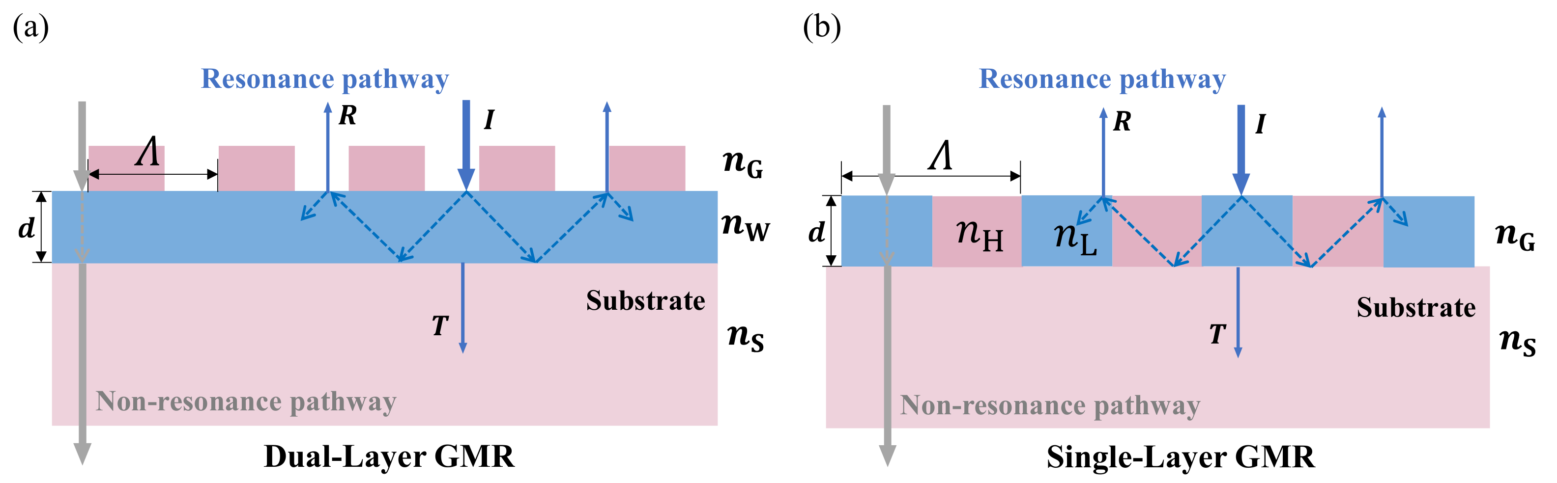
2.1. Guided-Mode Resonance

As mentioned before, GMR is a fundamental principle used to design metasurfaces with high reflectivity [23]. Figure 1a presents the schematic of a dual-layer GMR, a grating layer ( n G layer), and a waveguide layer ( n W layer), with a normal incident light at the intensity of I and its reflected and transmitted light (in solid blue). The incident light is first diffracted by the grating layer, and is coupled into the waveguide layer (in dashed blue) when it meets the resonance condition. Here, GMR occurs because the incident light and the waveguide mode constructively interference, resulting in the reflectivity R approaching near-unity and the transmission T near-zero. Otherwise, the light transports directly through the two functional layers as well as the substrate ( n S layer) (in solid gray). There is another way of realizing GMR by using a single-layer configuration as illustrated in Figure 1b. The grating layer can also act as the waveguide as long as the higher refractive index of the grating n H , the lower index n L , and optical thickness d of the grating structure are carefully optimized [24,42,43]. Here, n G represents the effective refractive index of the same layer of the grating and the waveguide. The single-layer GMR configuration can simplify the metasurface structure and facilitate the dissipating of heat [20,24].
The metasurfaces, commonly seen as a semi-finite-thickness slab, can be treated as an effective homogeneous medium, with the effective complex permittivity ε and the effective permeability μ expressed as ε + i ε and μ + i μ , respectively [44]. Following the effective medium theory, the perfect reflection can be achieved while Equation (1a) and (1b) are satisfied.
ε / μ < 0
ε μ = ε μ
The first condition in Equation (1a) requires the real parts of the permittivity and permeability to have opposite signs, which is easily satisfied at the resonate wavelength of electric or magnetic resonances. Although the second condition in Equation (1b) appears more strict, it can be satisfied at certain conditions. In particular, it is more easily satisfied in all-dielectric materials with low loss since the imaginary parts of ε and μ are approaching zero [17,18]. Therefore, we can verify whether our design is indeed a perfect reflector judging by the two conditions above, of which the permittivity ε and permeability μ can be extracted from the S-parameter via simulation [28,29,30,31].
As mentioned before, the SCDs are the perfect candidate for the grating layer for a metasurface reflector that can endure high-power lasers, but the materials for the substrate should also be thoroughly considered in order to meet our purpose. We propose the single-layer GMR configuration using SCDs as the resonant layer with the effective index denoted as n G . Here, the high refractive index equals that of the SCDs, i.e., n H = n SCD , and the low refractive index is that of the air ( n L = n air ). And in this paper, we choose the fused silica (silicon dioxide, SiO 2 ) as the substrate mainly for the two reasons below. First, its refractive index is lower than that of SCDs, meeting the conditions of the GMR theory. And second, silica has relatively high LIDT due to its extremely low thermal expansion coefficient, making it possible to be used for high-power-laser applications [45]. Last but not least, the diamond coating on SiO 2 substrates can be achieved using Microwave Plasma Chemical Vapor Deposition technique (MPCVD) [46].

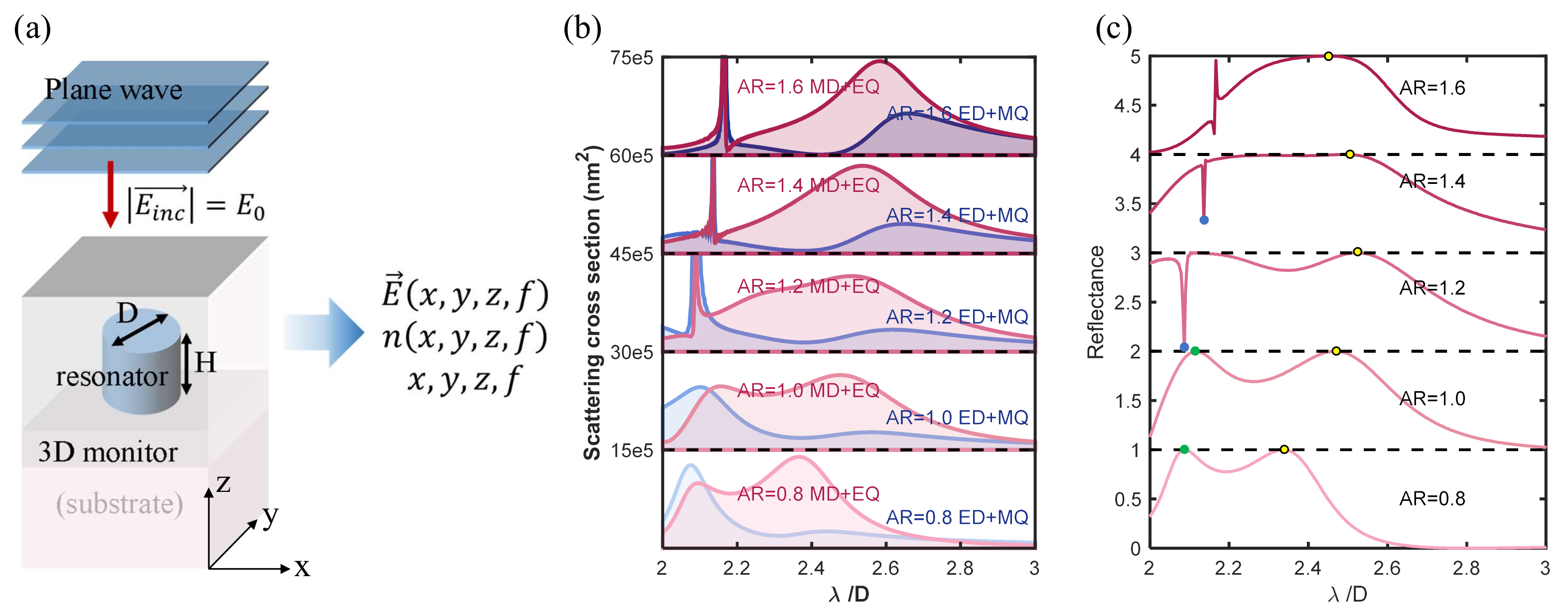
2.2. The Multipole Decomposition

To fully understand the behavior of light scattering and reflection in these resonant structures, it is essential to decompose the scattering field into multipole components for the complexity of the electromagnetic field [34]. Multipole decomposition is a crucial method for analyzing the complex electromagnetic fields of scattering, which can separate the contributions of electric dipole (ED), magnetic dipole (MD), electric quadrupole (EQ), magnetic quadrupole (MQ), and higher-order multipoles. It effectively simplifies the description of the field, facilitating the analysis of the field distribution, which helps guide the design of highly reflective metasurfaces [34,47,48].
The electric far-field scattered by an electric and a magnetic dipole (scalar projection) can be written as Equations (2a) and (2b) [47].
E ED z = E p e i π e i ω ED t z z k ED z
E MD z = E m e i π θ z e i ω MD t z z k MD z
E p ( E m ) represents the amplitudes of the fields scattered by electric (magnetic) dipoles. The phase factor e i π accounts for a phase shift observed during dipole excitation at resonance. The function θ [ z ] is a Heaviside step function, i.e., θ [ z ] = 0 for z < 0 and θ [ z ] = 1 for z > 0 , which describes the antisymmetric behavior of the magnetic dipole resonance [47]. The functions E ED ( z ) and E MD ( z ) present the properties shown below:
E ED ( z ) = E ED ( z )
E MD ( z ) = E MD ( z )
The incident field E 0 interacts with the scattered field E p or E m , ending up with interference. When E 0 = E p or E m , the destructive interference occurs in the forward (transmitted) direction, and a standing wave is generated in the backward (reflected) direction. In particular, when only ED and MQ contribute to the scattering field, the node of the standing wave is exactly at the surface of the reflector, exhibiting the same behavior of a perfect electric conductor (PEC), and therefore it can also be defined as the generalized electric mirror. In contrast, when the contribution purely comes from MD and EQ, an anti-node (instead of a node) should form at the surface of the mirror, which is referred to as the generalized magnetic mirrors [27,47].
Here, we start from the simplest cylindrical geometry structure of diamond metasurfaces, seen in Figure 2a. According to [49], the resonance wavelengths of ED and MD in a cylindrical resonator depend on the aspect ratio ( A R ), which is defined as A R = H / D , where H and D represent the height and diameter of the cylinder, respectively. Here, the simulations are conducted by 3D finite-difference time-domain solvers (FDTD, Lumerical Solutions, Inc., Canada), and a total field scattered field (TFSF) source is used to analyze the scattering properties. The SCSs along with the wavelength λ can be numerically calculated, and the peaks are shown at certain wavelengths, representing electric or magnetic resonance. By analyzing the wavelength difference of the reflective peaks, an optimized geometry is determined with H = 370   n m and P = 900   n m , where P (pitch) represents the center-to-center distance between adjacent diamond columns. Figure 2b illustrates the SCS for a diamond cylinder resonator without a substrate, with A R ranging from 0.8 to 1.6. The calculation of the SCS relies on Hinamoto’s work [32], and it requires the results of electric fields and refractive indices, which vary with the spatial position (x, y, z) and the light frequency f. Shown in Figure 2b, the resonant modes happen at the certain wavelength peaks (see Table S1 in the Supplementary Materials), forming either a generalized electric mirror (generated by ED+MQ) or a generalized magnetic mirror (generated by MD+EQ).
To further investigate the collective response of the diamond resonators, the reflective spectra at the square-latticed configuration are calculated as shown in Figure 2c. Corresponding to the SCSs, these illustrate that the yellow points of high-reflectivity are mainly the results of MD+EQ, while the peaks in green are the results of both ED+MQ and MD+EQ. However, for A R = 1.2 and 1.4 , there are sharp drops in the spectra at λ / D around 2.1. This is because the radiation fields destructively interfere, resulting from the similar far-field scattering patterns of ED+MQ and MD+EQ, which can be viewed as an anapole mode [35]. This mode can lead to the energy being localized in the resonators without emitting electromagnetic radiation, as well as a high Q-factor, with potential applications in optical trapping or certain types of lasers [36,37,50].

3. Results and Analysis

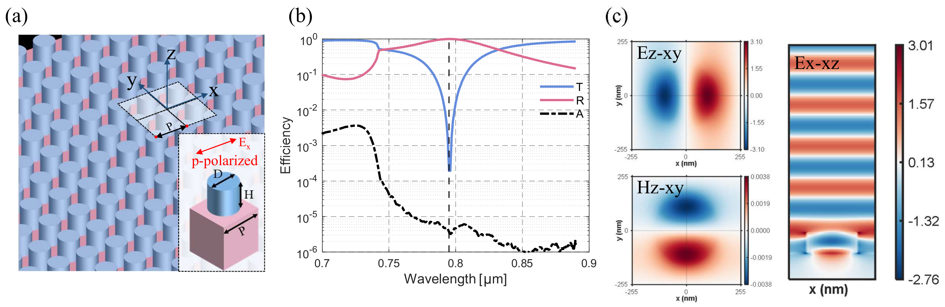
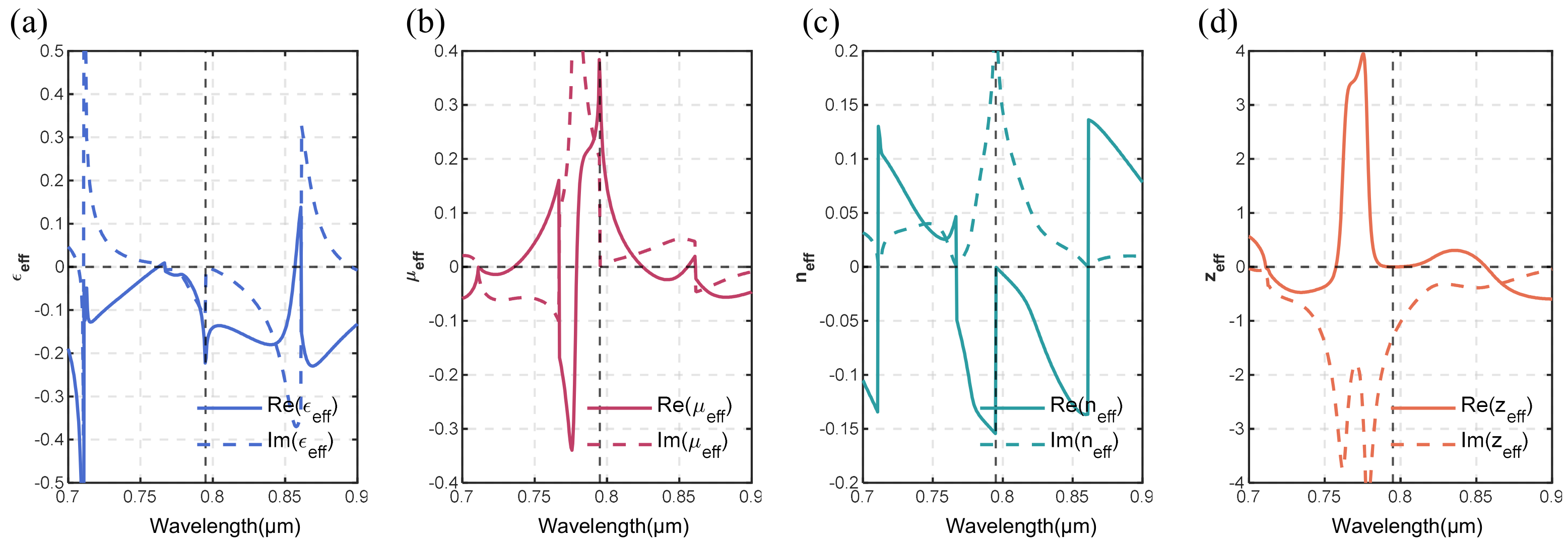
3.1. Cylindrical Resonators in Square Lattices

Based on the guidelines above, we can begin to design our all-dielectric metasurfaces with high reflectivity by using diamond resonators and silica substrates. Figure 3a shows the schematic of the diamond cylindrical resonators in square lattices. Simulations were performed at vertical incidence for p-polarized planewave at the wavelength between 700 n m and 890 n m . Figure 3b presents the efficiencies of reflectivity, transmission, and absorption along with the wavelength at the optimized parameters of D = 304     n m , H = 400     n m and P = 510     n m , which are determined by trial and error. It is clearly seen that at 795 n m , the reflectivity exceeds 99.99%, and absorbance is below 0.001%, behaving as a perfect reflector. The electromagnetic fields at 795 n m are calculated as displayed in Figure 3c. It shows the electric field E z (left-top) and magnetic field H z (left-bottom) in the xy-plane, revealing the simultaneous presence of both ED and MD resonances, respectively. The right diagram in Figure 3c presents the E x field in the xz-plane, and a half-wave loss in the backward propagation direction is observed here [27]. Therefore, ED is the main contribution of the scattering field, where the metasurface exhibits the behavior of an electric mirror. Additionally, the field enhancement is predominantly localized within the diamond resonators. This reveals that most of the electromagnetic energy is confined in the diamond layer, rather than being dissipated into the silica substrate, which can minimize thermal damage that might affect the metasurface performance.
Then, we calculate the effective medium properties of the functional layer by S-parameters in the FDTD solver. The results are shown in Figure 4, with the effective permittivity ( ε = ε + i ε ), magnetic permeability ( μ = μ + i μ ), refractive index ( n = n + i n ), and impedance ( z = z + i z ). Figure 4a,b show that for the wavelength near 795 n m , ε < 0 and μ > 0 , so the condition for perfect reflection in Equation (1a) is satisfied. Meanwhile, the imaginary parts ε and μ change the signs at the resonance wavelength 795 n m so that ε and μ are purely real; this meets the condition in Equation (1b). As shown in Figure 4c, the imaginary part of the refractive index ( n ) is proved to be maximized to prevent evanescent tunneling across the slab, while the real part of the refractive index ( n ) equals zero. In Figure 4d, we also note that the real part of the impedance approaches zero at 795 n m , which corresponds to a reflectivity of unity.
To analyze the impact of structural errors on the reflection spectrum, we conduct parameter sweeping for the three structural parameters (H, D, and P) at the range of 700 n m to 890 n m , and the reflective spectra results are shown in Figure 5. As shown in Figure 5a, the reflectivity is higher than 98 % when H is between 360 n m and 470 n m , providing high tolerance for the thickness of the diamond film. It is advantageous for fabrication because the highly precise control of cylindrical height is costly, as the realization of the film requires the heteroepitaxial growth in SCDs on a silica substrate. In contrast, the high-reflectivity peak redshifts to a significant degree with the growth in P and a given pitch P supports only a single resonance mode as seen in Figure 5b. Figure 5c shows that variations in cylinder diameter D result in multiple reflective peaks, each representing a different resonance mode. During the etching process in fabrication, P can be controlled with relatively high precision, while the cylinder diameter D is easily influenced by the vertical precision of etching processes. Therefore, more precise control of D is needed.

3.2. Frustums in Hexagonal Lattices

In order to mimic the vertical errors of the cylindrical etching processes, the resonators often adopt a frustum shape with a smaller top and larger base, rather than maintaining a perfectly cylindrical profile [19]. On the other hand, the hexagonal lattice exhibiting six-fold symmetry (C6) has higher symmetry, resulting in the advantages of compactness, wide-angle response, and broad photonic bandgap, compared with the square lattices, which possess only four-fold symmetry (C4) [21,51,52]. Consequently, we ultimately design a metasurface reflector based on the hexagonal lattices of diamond frustums, and the schematic is shown in Figure 6a. Here, P is the distance of adjacent frustums, while H, D top and D bot represent the height, the top diameter, and bottom diameter of the frustum.
Simulations were performed at vertical incidence for p-polarized planewave at the wavelength between 700 n m and 900 n m . Figure 6b presents the efficiencies of reflectivity, transmission, and absorption along with the wavelength at the optimized parameters of D top = 292   n m , D bot = 318   n m , H = 400   n m and P = 552   n m . It is clearly seen that at 795 n m , the reflectivity exceeds 99.99% and absorbance is below 0.001%, behaving as a perfect reflector.
To further analyze the impact of structural errors on the reflection spectrum, we conduct parameter sweeping for the structural parameters H and D gap (see Equation (4b)) at the range of 700 n m to 890 n m , and the reflective spectra results are shown in Figure 6c,d.
D avg = D top + D bot 2
D gap = D bot D avg = D avg D top
From Figure 6c, the spectral position of the resonance redshifts with H is growing but also remains greater than 98 % in the range of 370–500 nm, which has a better robustness to the cylinders in square lattices. However, as shown in Figure 6d, when we make D avg (see Equation (4a)) constant, the spectrum changes little when D gap is less than 50 nm. For frustums, the errors of D top and D bot come from the lack of precision in the electron beam lithography and etching process. But by slightly changing the input diameter of the cylinders, we can make D avg equal to the theoretical value of D, in order to compensate for the resonance shift induced by machining errors.

3.3. Dual-Band High Reflectivity

The metasurface can not only be designed for single-peak high reflectivity but can also be optimized for dual-band high reflectivity, holding the potential for applications that utilize lasers at two or more wavelengths, e.g., optical tweezers [53]. Here, we focus on cylindrical diamond resonators in square lattices. After adjusting the geometries, we achieve near-unity reflectance at the wavelengths of 744 n m and 828 n m when D = 380   n m , H = 300   n m and P = 500   n m , and the reflective spectrum is shown in Figure 7a in a solid blue line. To further analyze the dual-band reflector, we compute the SCSs of the ED+MQ, MD+EQ and the combination of their total scattering as shown in Figure 7a. It is observed that the first reflection peak at 744 n m primarily corresponds to an electric resonance, while the second reflection peak at 828 n m is mainly due to a magnetic resonance.
To explain the high reflectance at the two wavelengths from the perspectives of electric and magnetic mirrors, we conduct electromagnetic field analysis at the reflective peaks. At 744 n m , the electric field E xz closely resembles the reflective behavior of PEC because the electric field reflected at the surface experiences a half-wave loss, which is presented in Figure 7b. In contrast, at the 828 n m wavelength, the magnetic mirror does not exhibit a half-wave loss as presented in Figure 7c.

4. Conclusions

In this paper, we have conducted the design and analysis of highly reflective all-dielectric metasurfaces based on SCD resonators via FDTD simulations. First, utilizing GMR theory and multipole decomposition, we have acquired the preliminary values of the geometrical parameters ( H = 370   n m and P = 900   n m ) in a single diamond cylinder resonator for high reflection at 795 n m . Then, we designed two single-peak highly reflective configurations. The first is based on cylindrical resonators in a square lattice, and we achieved near-unity reflectivity (greater than 99.99%) and minimal absorption (below 0.001%) after optimization ( D = 304   n m , H = 400   n m and P = 510   n m ), as the design behaves as a general electric mirror judging from the electromagnetic field. And considering the fabrication errors, we swept the geometries of H, P and D, and found that H has strong robustness to the reflection spectrum, tolerating an error of approximately 100 n m . The second is the frustum-shaped resonators in hexagonal lattices ( D top = 292   n m , D bot = 318   n m , H = 400   n m and P = 552   n m ), and it also achieved 99.99% reflectivity as well as good robustness of height H. Moreover, we found that the adjustment of D avg can compensate for the errors of cylindrical D. For the two designs above, the reflective spectra within our simulated wavelength range change slightly with the height H of the columns. It is a good robustness because in fabrication, the total thickness variation (TTV) is less than 30 nm (see Figure S1 in the Supplementary Materials). Finally, we demonstrated dual-band high-reflectivity metasurfaces at 744 n m and 828 n m based on cylinders in square lattices, which are mainly resulted by ED+MQ and MD+EQ resonances, respectively.
This work paves the way for low-loss all-dielectric reflective metasurfaces in high-power laser applications. For example, our method can be extended to other wavelengths, particularly in the infrared range, where a broader bandwidth is possible. Moreover, by selecting more complex pillar structures, such as cross-shaped or H-shaped columns, more design dimensions are provided, allowing for dual-band or even multiband frequency control [21]. Using materials with higher refractive indices, large-angle oblique incidence for mirrors with high reflectivity can also be achieved [19].

Supplementary Materials

The following supporting information can be downloaded at: https://www.mdpi.com/article/10.3390/photonics11111015/s1.

Author Contributions

Conceptualization, Z.X. (Zhongyang Xing) and Z.X. (Zhongjie Xu); formal analysis, J.Z.; methodology, J.L.; Software, J.L.; validation, Z.X. (Zhongyang Xing); data curation, J.L.; writing—original draft preparation, Z.X. (Zhongyang Xing) and J.L.; writing—review and editing, Z.X. (Zhongyang Xing) and J.L.; supervision, X.C., J.Z. and Z.X. (Zhongjie Xu); funding acquisition, J.Z. and Z.X. (Zhongyang Xing). All authors have read and agreed to the published version of the manuscript.

Funding

This research was supported by the National Natural Science Foundation of China (12204541), the Science and Technology Innovation Program of Hunan Province (2021RC3083), and the High-level Talents Programs of National University of Defense Technology.

Institutional Review Board Statement

Not applicable.

Informed Consent Statement

Not applicable.

Data Availability Statement

Data will be made available on request.

Acknowledgments

We thank Yueqiang Hu and Shaozhen Lou from Hunan University, Research Fellow. Mingcheng Panmai from Nanyang Technological University and Xinye Liao from National University of Defense Technology for the useful discussions.

Conflicts of Interest

The authors declare no conflicts of interest.

Abbreviations

The following abbreviations are used in this manuscript:
GMRGuided Mode Resonance
FDTDFinite-Difference Time-Domain
SCDSingle-Crystal Diamond
EDElectric Dipole
MDMagnetic Dipole
EQElectric Quadrupole
MQMagnetic Quadrupole
TFSFTotal Field Scattered Field
ARAspect Ratio
SCSScattering Cross-Section
PECPerfect Electron Crystallograph

References

  1. Zheludev, N.I.; Kivshar, Y.S. From Metamaterials to Metadevices. Nat. Mater. 2012, 11, 917–924. [Google Scholar] [CrossRef] [PubMed]
  2. Liu, Y.; Zhang, X. Metamaterials: A New Frontier of Science and Technology. Chem. Soc. Rev. 2011, 40, 2494. [Google Scholar] [CrossRef] [PubMed]
  3. Chen, W.T.; Zhu, A.Y.; Capasso, F. Flat Optics with Dispersion-Engineered Metasurfaces. Nat. Rev. Mater. 2020, 5, 604–620. [Google Scholar] [CrossRef]
  4. Chen, H.T.; Taylor, A.; Nanfang, Y. A Review of Metasurfaces: Physics and Applications. Rep. Prog. Phys. 2016, 79, 076401. [Google Scholar] [CrossRef] [PubMed]
  5. Quan, Y.; Qin, G.; Linsen, C.; Yi, Z.; Yuhang, Y.; Xun, C.; Shuming, W.; Shining, Z.; Zhenlin, W. Recent Advanced Applications of Metasurfaces in Multi-dimensions. Nanophotonics 2023, 12, 2295–2315. [Google Scholar]
  6. Fröch, J.E.; Huang, L.; Tanguy, Q.A.; Colburn, S.; Zhan, A.; Ravagli, A.; Seibel, E.J.; Böhringer, K.F.; Majumdar, A. Real Time Full-color Imaging in a Meta-optical Fiber Endoscope. eLight 2023, 3, 13. [Google Scholar] [CrossRef]
  7. Ren, H.R.; Fang, X.Y.; Jang, J.; Burger, J.; Rho, J.; Maier, S.A. Complex-Amplitude Metasurface-Based Orbital Angular Momentum Holography in Momentum Space. Nat. Nanotechnol. 2020, 15, 948. [Google Scholar] [CrossRef]
  8. Devlin, R.C.; Ambrosio, A.; Rubin, N.A.; Mueller, J.P.B.; Capasso, F. Arbitrary Spin-to–Orbital Angular Momentum Conversion of Light. Science 2017, 358, 896–901. [Google Scholar] [CrossRef]
  9. Zhang, Z.; Liu, Y.; Wang, Z.; Zhang, Y.; Guo, X.; Xiao, S.; Xu, K.; Song, Q. Folded Digital Meta-Lenses for On-Chip Spectrometer. Nano Lett. 2023, 23, 3459–3466. [Google Scholar] [CrossRef]
  10. Ni, Y.; Chen, S.; Wang, Y.; Tan, Q.; Xiao, S.; Yang, Y. Metasurface for Structured Light Projection over 120° Field of View. Nano Lett. 2020, 20, 6719–6724. [Google Scholar] [CrossRef]
  11. Joo, D.H.; Kang, M.S.; Park, S.J.; Yu, S.A.; Park, W.T. Fabrication Method of Flexible Strain Sensors with CNTs and Solvents. Sens. Actuators A Phys. 2022, 345, 113775. [Google Scholar] [CrossRef]
  12. Zuraiqi, K.; Zavabeti, A.; Allioux, F.M.; Tang, J.; Nguyen, C.K.; Tafazolymotie, P.; Mayyas, M.; Ramarao, A.V.; Spencer, M.; Shah, K.; et al. Liquid Metals in Catalysis for Energy Applications. Joule 2020, 4, 2290–2321. [Google Scholar] [CrossRef]
  13. Mostafavi, E.; Iravani, S. MXene-Graphene Composites: A Perspective on Biomedical Potentials. Nano-Micro Lett. 2022, 14, 130. [Google Scholar] [CrossRef] [PubMed]
  14. Yao, Y.; Lan, L.; Liu, X.; Ying, Y.; Ping, J. Spontaneous Growth and Regulation of Noble Metal Nanoparticles on Flexible Biomimetic MXene Paper for Bioelectronics. Biosens. Bioelectron. 2020, 148, 111799. [Google Scholar] [CrossRef]
  15. Kouediatouka, A.N.; Liu, Q.; Mawignon, F.J.; Wang, W.; Wang, J.; Ruan, C.; Yeo, K.F.H.; Dong, G. Sensing Characterization of an Amorphous PDMS/Ecoflex Blend Composites with an Improved Interfacial Bonding and Rubbing Performance. Appl. Surf. Sci. 2023, 635, 157675. [Google Scholar]
  16. Kuznetsov, A.I.; Miroshnichenko, A.E.; Brongersma, M.L.; Kivshar, Y.S.; Luk’yanchuk, B. Optically Resonant Dielectric Nanostructures. Science 2016, 354, aag2472. [Google Scholar] [CrossRef]
  17. Slovick, B.; Yu, Z.G.; Berding, M.; Krishnamurthy, S. Perfect Dielectric-Metamaterial Reflector. Phys. Rev. B 2013, 88, 165116. [Google Scholar] [CrossRef]
  18. Moitra, P.; Slovick, B.A.; Gang Yu, Z.; Krishnamurthy, S.; Valentine, J. Experimental Demonstration of a Broadband All-Dielectric Metamaterial Perfect Reflector. Appl. Phys. Lett. 2014, 104, 171102. [Google Scholar] [CrossRef]
  19. Moitra, P.; Slovick, B.A.; Li, W.; Kravchencko, I.I.; Briggs, D.P.; Krishnamurthy, S.; Valentine, J. Large-Scale All-Dielectric Metamaterial Perfect Reflectors. ACS Photonics 2015, 2, 692–698. [Google Scholar]
  20. Atikian, H.A.; Sinclair, N.; Latawiec, P.; Xiong, X.; Meesala, S.; Gauthier, S.; Wintz, D.; Randi, J.; Bernot, D.; DeFrances, S.; et al. Diamond Mirrors for High-Power Continuous-Wave Lasers. Nat. Commun. 2022, 13, 2610. [Google Scholar] [CrossRef]
  21. Doiron, C.F.; Brener, I.; Cerjan, A. Realizing Symmetry-Guaranteed Pairs of Bound States in the Continuum in Metasurfaces. Nat. Commun. 2022, 13, 7534. [Google Scholar] [CrossRef] [PubMed]
  22. Magnusson, R.; Wang, S.S. New Principle for Optical Filters. Appl. Phys. Lett. 1992, 61, 1022–1024. [Google Scholar] [CrossRef]
  23. Wei, C.; Liu, S.; Deng, D.; Shen, J.; Shao, J.; Fan, Z. Electric Field Enhancement in Guided-mode Resonance Filters. Opt. Lett. 2006, 31, 1223–1225. [Google Scholar] [CrossRef] [PubMed]
  24. Sang, T.; Wang, Z. Study on Guided-Mode Resonance Optical Devices; Tongji University Press: Shanghai, China, 2020. [Google Scholar]
  25. Lin, D.; Fan, P.; Hasman, E.; Brongersma, M.L. Dielectric Gradient Metasurface Optical Elements. Science 2014, 345, 298–302. [Google Scholar] [CrossRef]
  26. Liu, W.; Kivshar, Y.S. Generalized Kerker Effects in Nanophotonics and Meta-Optics [Invited]. Opt. Express 2018, 26, 13085. [Google Scholar] [CrossRef]
  27. Liu, W. Generalized Magnetic Mirrors. Phys. Rev. Lett. 2017, 119, 123902. [Google Scholar] [CrossRef]
  28. Smith, D.R.; Schultz, S.; Markoš, P.; Soukoulis, C.M. Determination of Effective Permittivity and Permeability of Metamaterials from Reflection and Transmission Coefficients. Phys. Rev. B 2002, 65, 195104. [Google Scholar] [CrossRef]
  29. Smith, D.R.; Schurig, D. Electromagnetic Wave Propagation in Media with Indefinite Permittivity and Permeability Tensors. Phys. Rev. Lett. 2003, 90, 77. [Google Scholar] [CrossRef]
  30. Smith, D.R.; Vier, D.C.; Koschny, T.; Soukoulis, C.M. Electromagnetic Parameter Retrieval from Inhomogeneous Metamaterials. Phys. Rev. E 2005, 71, 036617. [Google Scholar] [CrossRef]
  31. Arslanagic, S.; Hansen, T.V.; Mortensen, N.A.; Gregersen, A.H.; Sigmund, O.; Ziolkowski, R.W.; Breinbjerg, O. A Review of the Scattering-Parameter Extraction Method with Clarification of Ambiguity Issues in Relation to Metamaterial Homogenization. IEEE Antennas Propag. Mag. 2013, 55, 91–106. [Google Scholar] [CrossRef]
  32. Hinamoto, T.; Fujii, M. MENP: An Open-Source MATLAB Implementation of Multipole Expansion for Nanophotonics. OSA Contin. 2021, 4, 1640. [Google Scholar] [CrossRef]
  33. Alaee, R.; Rockstuhl, C.; Fernandez-Corbaton, I. An Electromagnetic Multipole Expansion beyond the Long-Wavelength Approximation. Opt. Commun. 2018, 407, 17–21. [Google Scholar] [CrossRef]
  34. Terekhov, P.D.; Babicheva, V.E.; Baryshnikova, K.V.; Shalin, A.S.; Karabchevsky, A.; Evlyukhin, A.B. Multipole Analysis of Dielectric Metasurfaces Composed of Nonspherical Nanoparticles and Lattice Invisibility Effect. Phys. Rev. B 2019, 99, 045424. [Google Scholar] [CrossRef]
  35. Miroshnichenko, A.E.; Evlyukhin, A.B.; Yu, Y.F.; Bakker, R.M.; Chipouline, A.; Kuznetsov, A.I.; Luk’yanchuk, B.; Chichkov, B.N.; Kivshar, Y.S. Nonradiating Anapole Modes in Dielectric Nanoparticles. Nat. Commun. 2015, 6, 8069. [Google Scholar] [CrossRef]
  36. Conteduca, D.; Brunetti, G.; Barth, I.; Quinn, S.D.; Ciminelli, C.; Krauss, T.F. Multiplexed Near-Field Optical Trapping Exploiting Anapole States. ACS Nano 2023, 17, 16695–16702. [Google Scholar] [CrossRef]
  37. Tripathi, A.; Kim, H.R.; Tonkaev, P.; Lee, S.J.; Makarov, S.V.; Kruk, S.S.; Rybin, M.V.; Park, H.-G.; Kivshar, Y. Lasing Action from Anapole Metasurfaces. Nano Lett. 2021, 21, 6563–6568. [Google Scholar] [CrossRef]
  38. Holly, C.; Traub, M.; Hoffmann, D.; Widmann, C.; Brink, D.; Nebel, C.E.; Gotthardt, T.; Sözbir, M.C.; Wenzel, C. Monocrystalline CVD-Diamond Optics for High-Power Laser Applications. In Proceedings of the High-Power Laser Materials Processing: Lasers, Beam Delivery, Diagnostics, and Applications V, San Francisco, CA, USA, 13–18 February 2016. [Google Scholar]
  39. Krupke, W.F. Diode Pumped Alkali Lasers (DPALs)—A Review (Rev1). Prog. Quantum Electron. 2012, 36, 4–28. [Google Scholar] [CrossRef]
  40. Li, Y.; Wang, H.; Yang, Z.; Hua, W. Signal Broad Area High Power Laser Diode with Narrowed Linewidth. Laser Optoelectron. Prog. 2011, 48, 36–39. [Google Scholar]
  41. Cheng, H.; Wang, Z.; Zhang, F.; Tian, Z.; Cui, D.; Xu, Z. Research Development of Alkali Vapor Lasers. Laser Optoelectron. Prog. 2015, 52, 020002. [Google Scholar] [CrossRef]
  42. Magnusson, R.; Ding, Y. Spectral-Band Engineering with Interacting Resonant Leaky Modes in Thin Periodic Films. Proc. SPIE 2004, 5720, 119–129. [Google Scholar]
  43. Sang, T.; Wang, Z.; Wang, L.; Wu, Y.; Chen, L. Resonant Excitation Analysis of Sub-Wavelength Dielectric Grating. J. Opt. A: Pure Appl. Opt. 2006, 8, 62–66. [Google Scholar] [CrossRef]
  44. Lalanne, P.; Lemercier-Lelanne, D. Depth Dependence of the Effective Properties of Subwavelength Gratings. J. Opt. Soc. Am. A 1997, 14, 450–458. [Google Scholar] [CrossRef]
  45. Yu, X.; Yang, W.; Shen, C.; Tao, W.; Deng, X. Polarization Beam Combining by Fused Silica Subwavelength Grating. Opt. Commun. 2024, 554, 130135. [Google Scholar] [CrossRef]
  46. Li, Y.; Hao, X.; Dai, B.; Shu, G.; Zhao, J.; Zhang, S.; Liu, X.; Wang, W.; Liu, K.; Cao, W.; et al. Research Progress on High Rate and High Quality Growth of MPCVD Single Crystal Diamond. J. Synth. Cryst. 2020, 49, 979–989. [Google Scholar]
  47. Kruk, S.; Kivshar, Y. Tailoring Transmission and Reflection with Metasurfaces. In Dielectric Metamaterials; Elsevier: Amsterdam, The Netherlands, 2020; pp. 145–174. [Google Scholar]
  48. Savinov, V.; Fedotov, V.A.; Zheludev, N.I. Toroidal Dipolar Excitation and Macroscopic Electromagnetic Properties of Metamaterials. Phys. Rev. B 2014, 89, 205112. [Google Scholar] [CrossRef]
  49. Campione, S.; Liu, S.; Basilio, L.I.; Warne, L.K.; Langston, W.L.; Luk, T.S.; Wendt, J.R.; Reno, J.L.; Keeler, G.A.; Brener, I.; et al. Broken Symmetry Dielectric Resonators for High Quality Factor Fano Metasurfaces. ACS Photonics 2016, 3, 2362–2367. [Google Scholar] [CrossRef]
  50. Hsu, C.W.; Zhen, B.; Stone, A.D.; Joannopoulos, J.D.; Soljačić, M. Bound States in the Continuum. Nat. Rev. Mater. 2016, 1, 16048. [Google Scholar] [CrossRef]
  51. Vaidya, S.; Benalcazar, W.A.; Cerjan, A.; Rechtsman, M.C. Point-Defect-Localized Bound States in the Continuum in Photonic Crystals and Structured Fibers. Phys. Rev. Lett. 2021, 127, 023605. [Google Scholar] [CrossRef]
  52. Wang, X.; Wang, J.; Zhao, X.; Shi, L.; Zi, J. Realizing Tunable Evolution of Bound States in the Continuum and Circularly Polarized Points by Symmetry Breaking. ACS Photonics 2023, 10, 2316–2322. [Google Scholar] [CrossRef]
  53. Bustamante, C.J.; Chemla, Y.R.; Liu, S.; Wang, M.D. Optical Tweezers in Single-Molecule Biophysics. Nat. Rev. Methods Primers 2021, 1, 25. [Google Scholar] [CrossRef]
Figure 1. Dual-layer and single-layer GMR designs for high-reflectivity metasurfaces. (a) Schematic illustration of the dual-layer GMR design, where n G is the effective refractive index of grating layer, n W is the refractive index of the waveguide layer, and n S is for the substrate. The blue and gray lines show the pathway of resonance and non-resonance relatively. Here, Λ is the grating period, and d represents the thickness of the waveguide layer. I, R, and T are the intensity of the incident, reflected, and transmitted light. (b) The single-layer GMR structure where the grating layer functions as a waveguide layer as well. Here, n H is the higher refractive index, and n L is the lower.
Photonics 11 01015 g001
Figure 2. SCSs and reflectance spectrum of diamond resonators in square lattices by 3D FDTD solvers. (a) Schematic of the FDTD simulation setup for a single diamond resonator embedded in air, using a total field scattered field (TFSF) source to calculate the SCSs. (b) SCS of generalized electric mirror (ED+MQ) and magnetic mirror (MD+EQ) for A R = 0.8 , 1.0 , 1.2 , 1.4 , 1.6 . (c) Reflective spectrum of diamond resonators arrays in square lattices for A R = 0.8 , 1.0 , 1.2 , 1.4 , 1.6 .
Photonics 11 01015 g002
Figure 3. Cylindrical diamond resonators in square lattices. (a) Simulation schematic of diamond cylindrical resonators arranged in a square lattice, where D is the diameter of the cylinder, while H is the height, and P represents the distance of adjacent cylinders. (b) Reflectivity, transmission, and absorption plotted on a logarithmic scale with D = 304   n m , H = 400   n m and P = 510   n m . R is reflectance, T stands for transmittance, and A is absorption. (c) The electric field E z and magnetic field H z in the xy−plane, and the E x field in the xz−plane. Colors indicate the electric field amplitude.
Photonics 11 01015 g003
Figure 4. Effective medium properties of diamond metasurface mirror. (a) Effective permittivity ( ε eff ) as a function of wavelength. Re( ε eff ) represents the real part of ε eff , and Im( ε eff ) represents the imaginary part of ε eff . (b) Effective permeability ( μ eff ) as a function of wavelength. Re( μ eff ) represents the real part of μ eff , and Im( μ eff ) represents the imaginary part of μ eff . (c) Effective refractive index ( n eff ) as a function of wavelength. Re( n eff ) represents the real part of n eff , and Im( n eff ) represents the imaginary part of n eff . (d) Effective impedance ( z eff ) as a function of wavelength. Re( z eff ) represents the real part of z eff , and Im( z eff ) represents the imaginary part of z eff .
Photonics 11 01015 g004
Figure 5. Sweeping map of cylinder diamond resonators in square lattices at the wavelength between 700 nm and 890 nm. (a) Cylinder height from 200 nm to 600 nm. Colors indicate the reflectivity. (b) Pitch in the square lattice from 310 nm to 570 nm. (c) Cylinder diameter from 240 nm to 490 nm.
Photonics 11 01015 g005
Figure 6. Frustum-shaped diamond resonators in hexagonal lattices. (a) Simulation schematic of diamond frustum-shaped resonators arranged in a hexagonal lattice. Here, H is the height, and P represents the distance of adjacent frustums, while D top represents the top diameter of the frustum and D bot is the bottom. And D gap is the half of the difference of D top and D bot . (b) Reflectivity, transmission, and absorption plotted on a logarithmic scale with D top = 292   n m , D bot = 318   n m , H = 400   n m and P = 552   n m . (c) Sweeping map of frustum height, showing that the design remains robust within the height range of 380 nm to 480 nm. Colors indicate the reflectivity. (d) Sweeping map of D gap (half the gap between the top and bottom diameters of the frustum), showing how increasing the diameter affects the reflection spectrum.
Photonics 11 01015 g006
Figure 7. Cylindrical diamond resonators in square lattices and electric fields at two high-reflectivity wavelength, compared with PEC. (a) Reflectivity spectrum and SCS of ED+MQ and MD+EQ resonances, showing dual-band reflectivity peaks at 744 nm and 828 nm. (b) The electric field E x field in the xz−plane at 744 n m compared with PEC, showing a half-wave phase loss, indicating the behavior of a generalized electric mirror. (c) The electric field E x field in the xz−plane at 828 n m compared with PEC, showing a half-wave phase loss, where no half-wave phase loss is observed, demonstrating the characteristics of a generalized magnetic mirror.
Photonics 11 01015 g007
Disclaimer/Publisher’s Note: The statements, opinions and data contained in all publications are solely those of the individual author(s) and contributor(s) and not of MDPI and/or the editor(s). MDPI and/or the editor(s) disclaim responsibility for any injury to people or property resulting from any ideas, methods, instructions or products referred to in the content.

