Article

Structure Design of UVA VCSEL for High Wall Plug Efficiency and Low Threshold Current

1
Laboratory of Micro/Nano-Optoelectronics, Department of Microelectronics and Integrated Circuits, Xiamen University, Xiamen 361005, China
2
Institute of Nanoscience and Applications (INA), Southern University of Science and Technology (SUSTech), Shenzhen 518055, China
3
School of Optoelectronic Information, Minnan Science and Technology University, Quanzhou 362332, China
*
Authors to whom correspondence should be addressed.
Photonics 2024, 11(11), 1012; https://doi.org/10.3390/photonics11111012
Submission received: 23 September 2024 / Revised: 15 October 2024 / Accepted: 25 October 2024 / Published: 27 October 2024
(This article belongs to the Special Issue Next-Generation Vertical-Cavity Surface-Emitting Lasers)

Abstract

:
Vertical-cavity surface emitting lasers in UVA band (UVA VCSELs) operating at a central wavelength of 395 nm are designed by employing PICS3D(2021) software. The simulation results indicate that the thickness of the InGaN quantum well and GaN barrier layers affect the emission efficiency of UVA VCSELs greatly, suggesting an optimal thicknesses of 2.2 nm for the well layer and 2.7 nm for the barrier layer. Additionally, an overall consideration of threshold current, series resistance, photoelectric conversion efficiency, and optical output power results in the optimized thickness of the ITO current spreading layer, ~20 nm. Furthermore, by employing a five-pair Al0.15Ga0.85N/GaN multi-quantum barrier electron blocking layer (EBL) instead of a single Al0.2Ga0.8N EBL, the device shows a ~51% enhancement in the optical output power and a ~48% reduction in the threshold current. The number of distributed Bragg reflector (DBR) pairs also plays crucial roles in the device’s photoelectric performance. The device designed in this study demonstrates a minimum lasing threshold of 1.16 mA and achieves a maximum wall plug efficiency of approximately 5%, outperforming other similar studies.

1. Introduction

Vertical-cavity surface emitting lasers (VCSELs) have the advantages of single longitudinal mode output, low threshold current, low divergence output beam, high coupling efficiency with fiber, and easy two-dimensional array [1,2]. These characteristics make them well suited for a wide range of applications such as high-resolution laser displays, semiconductor lighting, data communication, and optical storage [3,4]. Over the past few decades, VCSELs based on GaAs and GaN have achieved remarkable research advancements in the infrared and visible wavelengths [5]. However, the development of ultraviolet (UV) VCSELs, which hold significant importance in areas like ultraviolet curing, medical treatment, and biological control, has been hindered due to difficulties in structural design, epitaxial growth, and device processes as well. So far, the existing UV VCSELs are all optically pumped and the lasing wavelengths are mainly concentrated in the UVA band (320–400 nm) [6,7,8,9,10,11], with no reports of UV electrically pumped VCSELs. The reason lies in the necessity of AlGaN materials with high aluminum content for the UVB (280–320 nm) and UVC (200–280 nm) bands, leading to the increased complexity in developing high-quality AlGaN films. Until now, optically pumped UVA VCSELs are predominantly based on InxGa1−xN/GaN quantum well structures, with the shortest luminescence wavelength close to the GaN bandgap (~360 nm). The electrically injected UV VCSELs are still facing problems related to carrier injection efficiency, current spreading, and material self-absorption, posing significant obstacles to the development of UV devices [12,13,14,15].
Due to the complexity of the VCSEL structure, the performance of the device can be greatly improved through a reasonable structural design. The quantum well active region providing optical gain is the most important component of laser devices. Therefore, the optimization of active region is particularly important. In previous studies, Mei Zhou et al. utilized LASTIP software to investigate the influence of quantum well and barrier layer thickness on the performance of edge-emitting lasers, discovering that an appropriate increase in barrier layer thickness can effectively suppress carrier leakage [16]. K Meel et al. delved into the influence of quantum well and quantum barrier width on the optical and electrical characteristics of blue LEDs using device simulations [17]. However, there is still limited research on the investigation of active region structure of UV band VCSELs.
Furthermore, challenges such as material self-absorption and the design of an electron blocking layer (EBL) should also be carefully considered in UV band VCSELs because of the larger material absorption and shallower QWs when compared to devices emitting in the visible spectral range. Particularly, the absorption of distributed Bragg reflectors (DBRs) and Indium Tin Oxide (ITO) are significantly enhanced in the UV band. Lai and Konig et al. meticulously measured the absorption properties of ITO across diverse spectral ranges, unveiling a notable rise in the absorption coefficient within the UV band [18,19]. Haocheng Wu et al. identified the definite influence of the pair number in the DBRs on the optical performance of Resonant-Cavity Light-Emitting Diodes (RCLEDs) [20]. Additionally, in tackling the issue of carrier leakage, the integration of an EBL between the active region and p-GaN, such as an Al-graded bulk AlGaN EBL, ternary InAlN EBL, and AlGaN/GaN uniform multiple quantum barrier (UMQB) EBL, has been demonstrated to be effective [21,22,23,24].
In this study, we utilized PICS3D(2021) software to design an electrically injected UVA VCSEL with a central wavelength of 395 nm and a cavity length of 5 λ , since there is still no report on electrical-driven VCSELs in the wavelengths below 400 nm. The thickness and structure of the active region, current spreading layer, and EBL were systemically optimized. Both the thickness of the QW and QB layers show a great influence on the output power and threshold current of the UVA VCSEL. The optimized device with three pairs of InGaN(2.2 nm)/GaN (2.7 nm) MQW active regions shows the best performance. Additionally, the thickness of ITO and the pair number of DBRs also significantly impact the optical and electrical characteristics of VCSEL devices. The optimized ITO thickness is ~20 nm and the pair number turns out to be 9 and 18.5 for the top DBR and the bottom DBR, respectively. It is also found that the utilization of MQB EBL instead of a single AlGaN layer results in a remarkable ~51% increase in the output power and a substantial ~48% decrease in the threshold current.

2. Device Structure and Simulation Method

Figure 1 illustrates the two-dimensional and three-dimensional structural diagrams of the UVA VCSEL with a double dielectric DBR structure utilized for simulation in this study. The basic model of the device consists of n-GaN with a doping concentration of 5 × 1018 cm−3, 3 pairs of In0.08Ga0.92N/GaN quantum well active regions, an Al0.2Ga0.8N EBL with a doping concentration of 3 × 1017 cm−3, p-GaN with a doping concentration of 5 × 1017 cm−3, and an ITO current spreading layer. The device features a current confinement aperture with a diameter of 5 μ m and lasing wavelength of 395 nm. The detailed structural parameters are provided in Table 1 under optimal device performance conditions.
PICS3D (2021) software (Crosslight Company) was used for conducting simulation calculations [25,26]. By leveraging finite element analysis, it addresses the Poisson equation, current continuity equation, carrier transport equation, complex wave equation, and laser rate equation of VCSEL in cylindrical coordinate system, enabling an accurate calculation of the electrical and optical characteristics of the semiconductor laser. Additionally, the spontaneous polarization and piezoelectric polarization of GaN-based materials are also considered in the simulator; they jointly determine the overall polarization direction and the total built-in electric field within the material, significantly impacting the emission wavelength and luminous efficiency of the light-emitting device. Simulation models include the carrier drift-diffusion (DD) model, the self-consistent multi-quantum well model, the optical waveguide model, and the effective index model (EIM) [27]. In the simulation, the Auger recombination coefficient and Shockley–Read–Hall (SRH) recombination lifetime are set to be 1.4 × 10⁻³¹ cm6/s and 10−8 s, respectively [28,29]. The polarization ratio is set to be 40% for calculating the polarization electric field of III-nitride-based devices [30]. The conduction/valence band offset ratio was set to be 70:30 for MQWs and 50:50 for AlGaN/GaN interface [31]. The mobility of the electron and hole is 100 cm2/V · s and 10 cm2/V · s [32], respectively. To account for optical losses, the absorption coefficient of ITO is 4000 cm−1 [18,19] and the average optical background loss of the n-GaN, MQWs, EBL, and p-GaN layers in the cavity was set to 10 cm−1 [33]. The detailed physical parameters of simulation are listed in Table 2.
To validate the accuracy of the model, we initially simulated the reference experimental device report by Kuramoto et al., as illustrated in Figure 2a,b [34]. The stimulated VCSEL has a laser wavelength of 441.9 nm and a gain peak of 442.1 nm. The device has a total cavity length of 5 λ and Table 3 presents the key material parameters utilized in both experiments and simulations. We utilized the WebplotDesigner tool to extract the power–current (PI) curve data from the actual devices presented in the referenced paper for comparison with our simulation data. As illustrated in the P-I curve in Figure 2c, there is a good agreement between the experimental results and our simulation outcomes, thereby validating the accuracy and effectiveness of our simulation procedure.

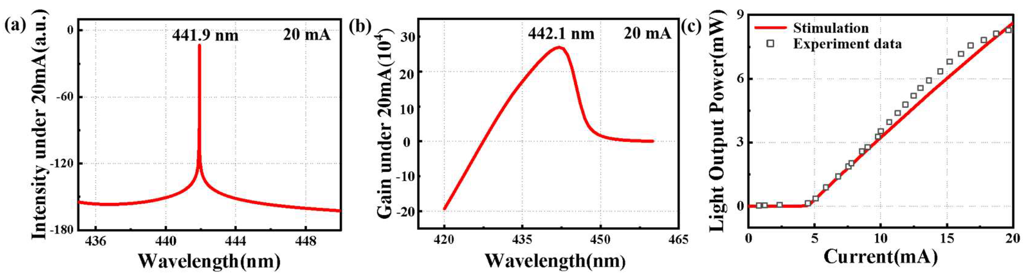
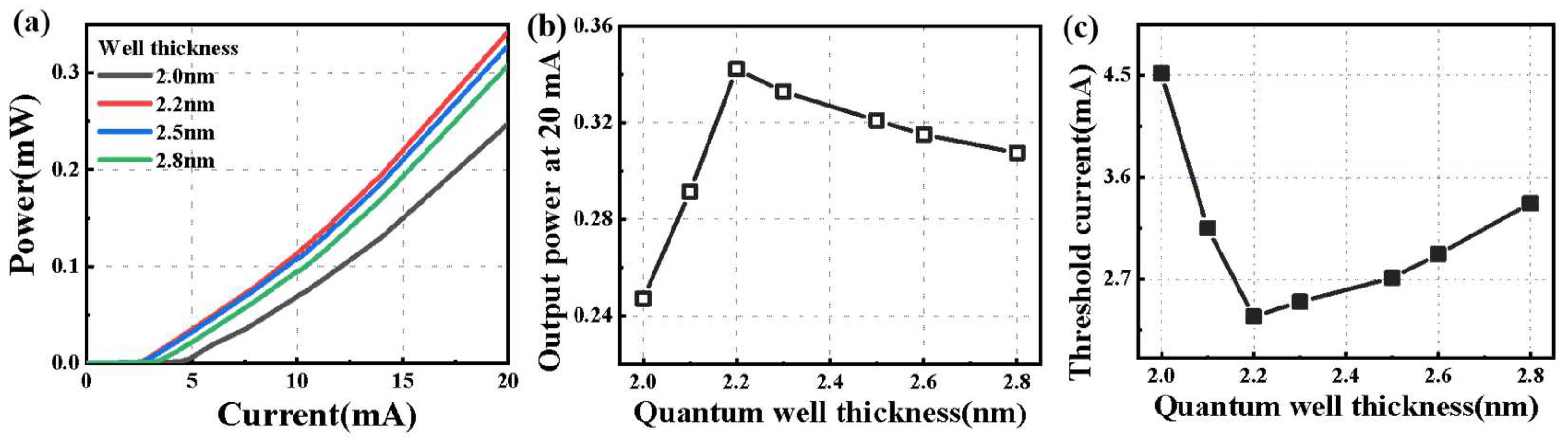
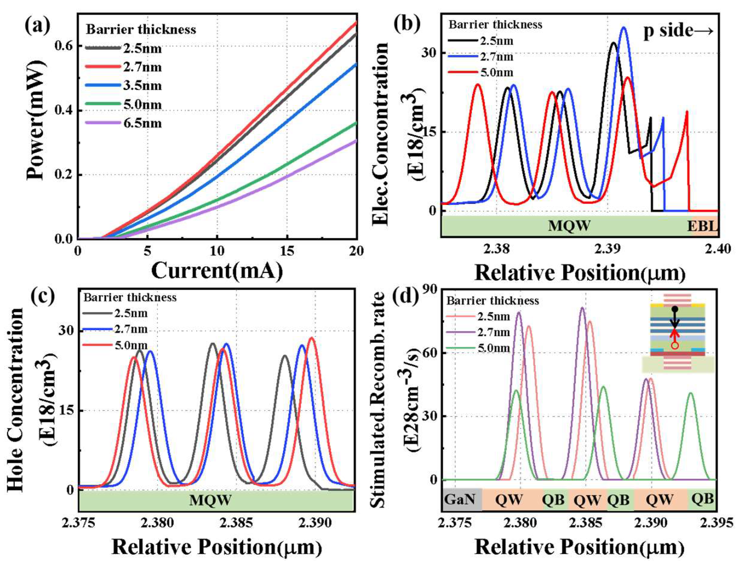
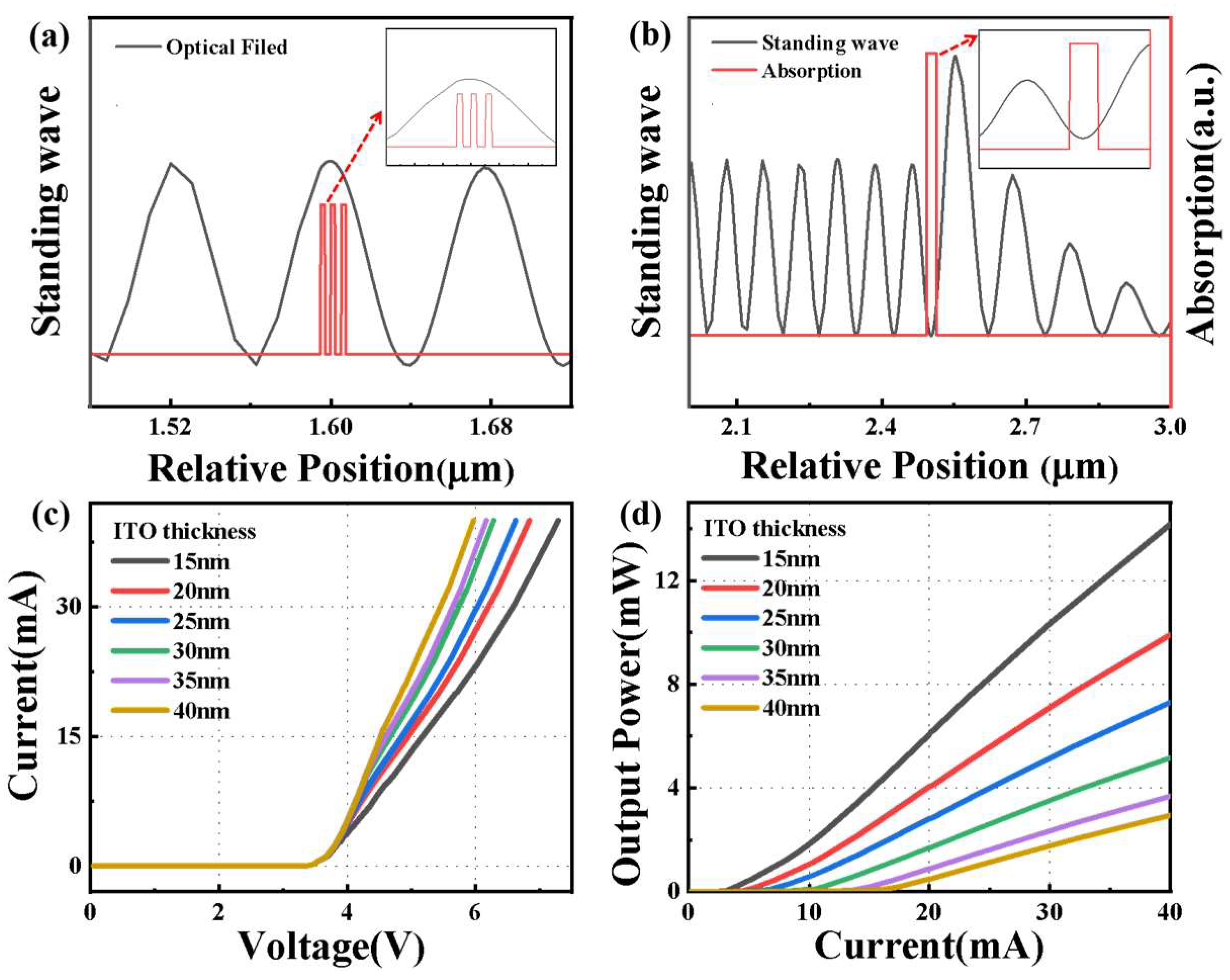
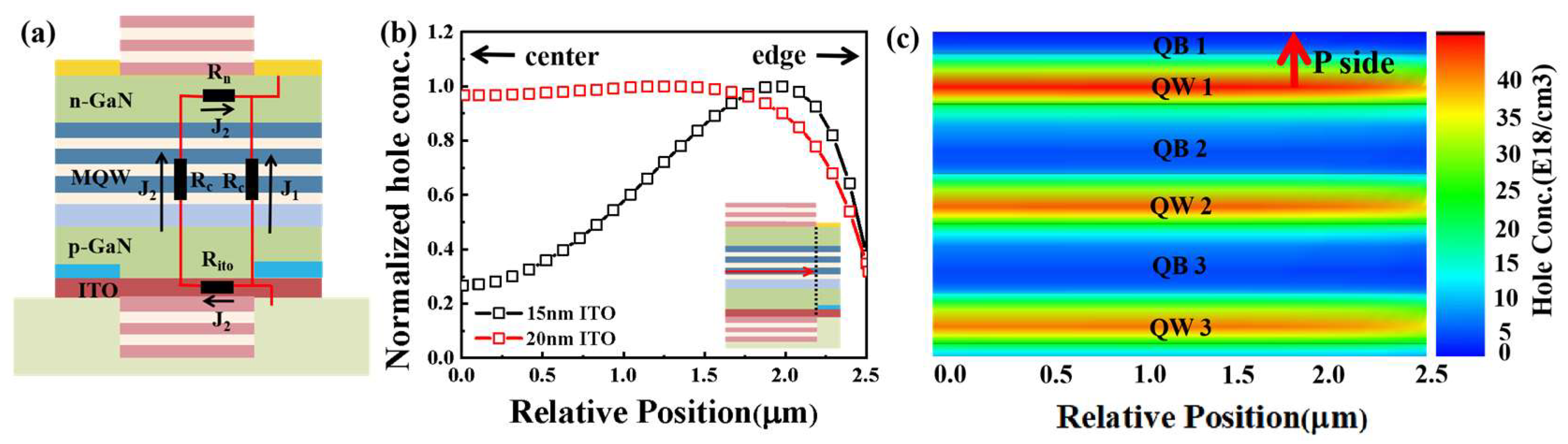
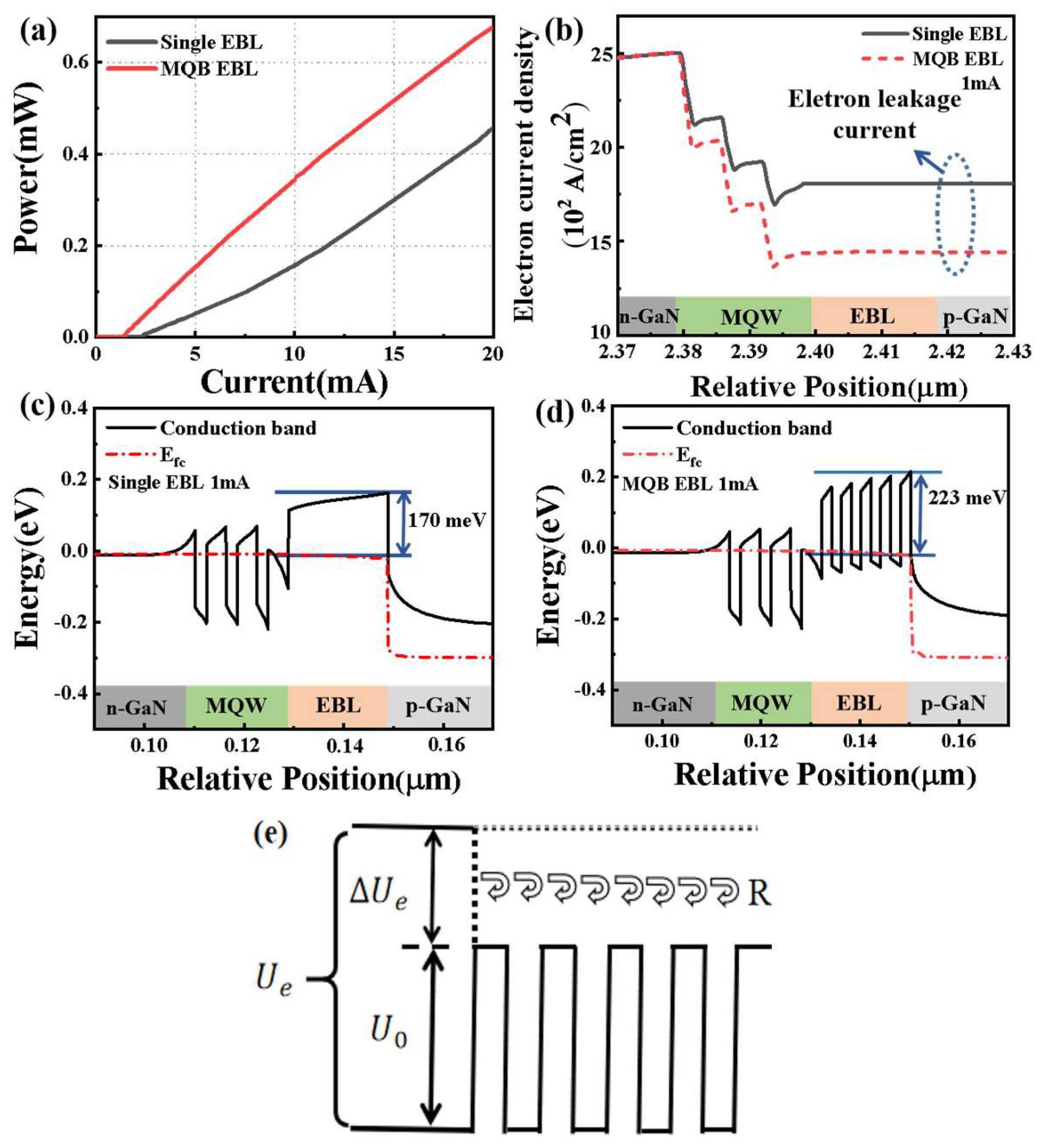
3. Results and Discussion

In comparison to conventional bulk materials, the gain of VCSEL devices can be significantly enhanced by utilizing the quantum well active region (QW) structure, resulting in a lower operating threshold. However, the thickness of the well layer and barrier layer within the active region profoundly influence the device’s performance. Therefore, we first the optimize quantum well structure for a 395 nm VCSEL. The active region adopts three pairs of In0.08Ga0.92N/GaN QWs because an excessive number of QWs can lead to an uneven carrier distribution, resulting in varied gains across the whole active region, and some of the QWs may even act as absorption layers [35]. Previous simulation results indicate that reducing the number of QWs can also decrease the lasing threshold current [36,37]. Figure 3 depicts the optical and electrical performance of the devices corresponding to different well layer thicknesses when the barrier layer thickness is 6.0 nm. The device QW thickness of 2.2 nm demonstrates the lowest threshold current and highest output power. Deviating from this optimal well thickness results in a decrease in output power and increase in threshold current.
To understand the influence of QW thickness on device performance, we calculated the electron concentration in the active region with thinner QWs with a well thickness of 2.0 nm, as shown in Figure 4a. A thinner quantum well leads to decreased electron concentrations when compared with the optimized well thickness of 2.2 nm. This finding suggests that electron confinement is weaker, and carrier leakage is more serious in a thinner QW. A decrease in the well thickness leads to an elevation in the ground state energy level, consequently reducing the energy gap between the ground state and the quantum barrier. Therefore, the energy required for electrons to escape from the well layer decreases, inducing larger carrier leakage from the QWs [38,39]. A QW that is too thick will also degrade the device’s performance. Figure 4b–d illustrate the overlap diagrams of electron and hole wave functions for well layer thicknesses of 2.2 nm, 2.5 nm, and 2.8 nm, respectively. It is apparent that the overlap degree of electron and hole wave functions decreases gradually as the thickness of the well layer increases. This phenomenon arises from the existence of the quantum-confined Stark effect (QCSE), which is caused by the polarization electric field-induced energy band tilt. The QCSE will be more serious in thicker QWs, leading to a reduction in the overlap of electron and hole wave functions, consequently deteriorating device performance.
Figure 5a shows the power–current characteristics of the VCSEL across different barrier thicknesses, and the well thickness was fixed to be 2.2 nm. The device shows the largest output power at a barrier thickness of 2.7 nm. Figure 5b,c show the electron and hole concentration in the MQWs with a barrier thickness of 2.5 nm, 2.7 nm, and 5.0 nm, respectively. While the barrier thicknesses is smaller than 2.7 nm, there is a tendency for electrons to accumulate in the QWs close to the p-side, and holes to accumulate in the QWs close to n-side, which is known as the “flyover” charge carrier process [40]. The deviation in spatial distribution of electrons and holes diminishes the efficiency of electron–hole radiation recombination, thereby deteriorating the luminous performance of the device. This conclusion is substantiated by the stimulated radiation recombination rates depicted at different barrier thickness in Figure 5d, and the arrows in the illustration represent the direction of electron and hole motion under an applied electric field. Nevertheless, the low mobility of holes hinders their migration into the n-side quantum wells when the barrier thickness significantly surpasses the optimal value. It has been reported in the literature that this will escalate the non-radiative recombination rate [41,42], thereby substantially affecting the emission performance of the active region and reducing the output power. For the UVA VCSEL with a central wavelength of 395 nm in this study, the optimal well layer and barrier layer thicknesses are determined to be 2.2 nm and 2.7 nm, respectively, which is consistent with the actual well layer thickness of the GaN laser, generally ranging from 2 to 3 nm [43].
The optimization of current spreading layer is also essential for GaN-based VCSELs in the UV band. ITO is commonly used as the current spreading layer on the p-side of GaN-based light emitting devices due to its excellent conductivity and optical transparency across the visible spectrum. Despite showing increased optical absorption losses in the near-ultraviolet range, studies have indicated that ITO can still achieve high transmittance at a wavelength of 395 nm [44,45], making it suitable for ohmic contact and current spreading in UVA VCSEL. However, the thickness of the ITO layer seriously impacts the optical and electrical properties of the VCSEL. Therefore, it is crucial to meticulously design the appropriate thickness of ITO to improve the performance of GaN-based lasers. The ITO absorption coefficient set in the simulation is 4000 cm−1, consistent with the results of prior studies by F. Lai and Konig [18,19,46].
The active region is positioned at the standing wave antinode to maximize the gain enhancement factor during simulation, as shown in Figure 6a. Additionally, it is essential that ITO is positioned at the standing wave node to minimize the optical absorption loss within the cavity, as illustrated in Figure 6b. Figure 6c shows the current–voltage (I-V) characteristic curves at different ITO thicknesses. As the thickness of ITO increases, the series resistance of the device decreases, attributed to the enhanced current spreading capability. Figure 6d presents the P-I curves for ITO thickness ranging from 15 nm to 40 nm. It is evident that the output power is significantly influenced by the ITO thickness. Figure 7a shows the variation in the output power as a function of the ITO thickness. It is clear that for every 10 nm increase in ITO thickness, the optical output power of the device shows a ~50% decrease. Meanwhile, the threshold current increases and photoelectric conversion efficiency (PCE) decreases with increasing ITO thickness, as shown in Figure 7b,c. These are caused by absorption of the ITO layer which results in optical absorption loss with increasing ITO thickness. Moreover, Figure 7d demonstrates a substantial decrease in series resistance as the ITO thickness increases from 15 nm to 40 nm. With the ITO thickness progressing from 20 nm to 30 nm, the reduction in series resistance becomes slower. Nevertheless, the changes in series resistance are less significant beyond 30 nm. Thus, taking into account the impact on the output power, lasing threshold, and series resistance, an ITO thickness of 20 nm proves to be a suitable selection for optimal device performance. Compared to the 15 nm ITO thickness, the device with a 20 nm ITO layer exhibits lower series resistance, which enhances the current spreading capacity within the device and helps alleviate heat-related problems during operation to a certain extent. To verify this point, we conducted the following theoretical analysis. Figure 8a presents the simplified equivalent circuit diagram of the VCSEL, where R n represents the transverse resistance of n-GaN, R i t o denotes the transverse resistance of ITO, and R c indicates the series resistance of n-GaN, MQW, and p-GaN. We define J 1 as the current density along the internal edge path of the device, and J 2 as the current density along the central path. The value of J 1 / J 2 is close to 1, meaning the current within the device is uniform, described by the following equation [47]:
J 1 J 2 = 1 + R n + R i t o R c
As the thickness of ITO increases, the transverse resistance R i t o decreases, resulting in the value of J 1 / J 2 decreasing and enhanced current spreading, which facilitates the injection of more holes into the device’s aperture center. Figure 8b presents the normalized hole concentration distribution along the lateral direction in the last quantum well of VCSELs with different ITO thicknesses at 4 mA, along with a diagram illustrating the hole extraction location. With a 20 nm ITO layer, the hole distribution is significantly more uniform, achieving a concentration of 97% in the center region, and the two-dimensional mapping of hole concentration in the active region is presented in Figure 8c. In contrast, the 15 nm ITO layer results in a hole distribution primarily concentrated at the edges of the device, leading to only a 27% concentration in the center region. These results further confirm the superior current spreading capabilities of the 20 nm ITO configuration.
Apart from active region and current spreading layer, the design of an EBL was also performed in this study. Due to the substantial difference in the effective mass between electrons and holes, electron leakage from the active region to the p-side is usually more serious in GaN-based light emitting devices, resulting in the degeneration of emission efficiency. To address this problem, an effective approach is to incorporate an electron blocking layer between the active region and p-GaN. In this study, we introduce a five-pair Al0.15Ga0.85N(2 nm)/GaN(2 nm) MQB EBL structure. For comparison, a simulation was also carried out using a single Al0.2Ga0.8N EBL. Figure 9a illustrates the alterations of the output power and threshold current of the device after the introduction of an MQB EBL. With the employment of the MQB EBL, the device’s output power at 20 mA increases from 0.45 mW to 0.68 mW, whereas the threshold current decreases from 2.30 mA to 1.19 mA when compared to the device with a single Al0.2Ga0.8N EBL. Simultaneously, Figure 9b demonstrates a notable reduction in the electron leakage current on the p-side of the device after the integration of the MQB EBL. This decrease is credited to the increased electron barrier height between the active region and EBL. As shown in Figure 9c,d, the electron barrier height is elevated from 170 meV to 223 meV after the introduction of the MQB EBL, thereby bolstering the electron-blocking effect. This result can be elucidated by the principles of quantum mechanics. As shown in Figure 9e, in the classical model, when the electron energy E surpasses the barrier height U 0 , the electron will inevitably move to the p-side. However, in quantum mechanics, there is a possibility that the incident electron will be reflected even if the electron energy exceeds the barrier height U 0 [48]. Furthermore, the incorporation of a periodic structure leads to the interference of electron waves reflected at each boundary, which enhances the reflectivity of the barrier and engenders an additional barrier height. Consequently, the accurate adjustment of quantum barriers and quantum wells thickness is crucial, requiring thorough consideration of the effective mass and barrier height of each layer. In this study, the thickness of the well layer and barrier layer conforms to the 2 nm/2 nm guidelines specified by D. H. Hsieh [27]. The results demonstrate a ~51% enhancement in the device output power and a ~48% reduction in the threshold current after the integration of the MQB EBL.
At last, the design of the DBR was performed for UVA VCSELs. In the UV band, double dielectric film DBRs consisting of HfO2 and SiO2 are commonly used as mirrors for the requirements of high reflectivity and low material absorption. However, the presence of defects and interface roughness in DBR can cause optical absorption and scattering losses, which reduce both reflectivity and the overall optical output power of the laser. Therefore, a sufficient pair of DBR layers is essential to achieve a reflectivity of at least 99%. Additionally, the absorption characteristics of these oxides in the UV range must also be taken into account. In this study, the absorption coefficient of HfO2 is specified as 0.346 cm−1 [49]. Subsequently, the optimal number of DBR pairs required for the device was calculated.
R = 1 ( n 1 / n 2 ) m ( n 1 2 / n s ) 1 + ( n 1 / n 2 ) m ( n 1 2 / n s ) 2
The reflectivity of the DBR is determined by Equation (2), where n 1 and n 2 denote the refractive indices of the two materials within the DBR, and m represents the pair of DBR film layers. When considering absorption losses, the refractive indices n1 and n2 of the two materials should be adjusted to their complex refractive indices n 1 and n 2 , given by n 1 = n 1 i α 1 and n 2 = n 2 i α 2 , where α 1 and α 2 are the absorption coefficients of the materials. Consequently, the reflectance formula is modified to Equation (3):
R = 1 ( n 1 / n 2 ) m ( n 1 2 / n s ) 1 + ( n 1 / n 2 ) m ( n 1 2 / n s ) 2
It is evident that the reflectivity of the DBR increases with an increase in the number of film layers according to Equation (2). However, due to the intrinsic absorption of the oxide material, a larger number of layers do not always lead to higher reflectivity. The outcomes depicted in Figure 10a indicate that beyond 18 pairs of DBR, further enhancement in the reflectivity is not obvious due to heightened material absorption. Therefore, the bottom DBR was set to 18.5 pairs in this study, including 0.5 pairs of a phase adjustment layer. On the other hand, considering the light output power (LOP), the reflectivity of the top DBR cannot be too high. Figure 10b shows the variation in LOP with different pairs of the top DBR. The data indicates that under high injection currents, the device’s LOP can be maximized by employing nine pairs of SiO2/HfO2 for the top DBR, and a maximum wall plug efficiency (WPE) of approximately 5% can be achieved, as depicted in Figure 10c. This optimal performance is attributed to the favorable balance between the reflectivity and mirror losses. A too-low reflectivity of the top DBR results in significant mirror losses and a much higher lasing threshold. Conversely, an excessive number of DBR pairs restricts the output optical power. Therefore, considering the material absorption characteristics in the ultraviolet spectrum, the pairs of the DBR should be reasonably designed, which can not only enhance the reflectivity of the DBR but also markedly improve the LOP of the device.
A comparison of reported simulation works on VCSELs with similar lasing wavelengths is presented in Table 4. In comparison to these studies, the VCSEL developed by us demonstrates easier attainment of low-threshold lasing, with thresholds as low as 1.19 mA (6.06 kA/cm2), and exhibits higher wall plug efficiency. These findings underscore that the accurate consideration of the active region and other layers is crucial to the successful design of UV electric pump VCSELs, thereby providing good guidance for the practical fabrication of UV electro-injected VCSELs.

4. Conclusions

In this study, a UVA VCSEL with a cavity length of 5 λ and a central wavelength of 395 nm was meticulously designed and optimized. The results demonstrate that the optimized QW and QB thickness are 2.2 nm and 2.7 nm, respectively. Considering the effects of threshold current, series resistance, photoelectric conversion efficiency, and optical output power, the optimal ITO thickness is ~ 20 nm. Additionally, the study identifies that substituting a single EBL structure with a MQB structure enhances the electron blocking effect, resulting in a ~51% increase in the laser output power and a ~48% reduction in the threshold current. It is also observed that pairs of DBR layers can affect both the reflectivity of the DBR and the optical output power of the laser. The optimal pairs of top and bottom DBRs are 9 and 18.5 pairs, respectively. The optimized UVA VCSEL enables an emission at a wavelength of 395.5 nm, with an optical output power of 12.76 mW at 40 mA, and a maximum wall plug efficiency of approximately 5%. Notably, the threshold current can be reduced to 1.19 mA (6.06 kA/cm²).

Author Contributions

Conceptualization, B.A., Z.Z. (Zhijie Zou). and B.Z.; data curation, B.A.; formal analysis, B.A. and Y.M.; investigation, B.A., Y.W. (Yukun Wang) and Y.W. (Yachao Wang); supervision, B.Z. and Y.M.; validation, B.Z. and Y.M.; visualization, B.A.; writing—original draft preparation, B.A., writing—review and editing, H.L., Z.Z. (Zhiwei Zheng), Y.M. and B.Z., project administration, B.A., Y.W. (Yukun Wang), Y.M. and B.Z.; funding acquisition, H.L., Z.Z. (Zhiwei Zheng), Y.M. and B.Z. All authors have read and agreed to the published version of the manuscript.

Funding

This work was supported by the National Natural Science Foundation of China (Nos. 62234011, U21A20493, 62174140 and 62104204) and Natural Science Foundation of Fujian Province (2023J05020).

Data Availability Statement

The data that support the findings of this study are available from the corresponding authors upon reasonable request.

Acknowledgments

We would like to acknowledge Crosslight corp. for providing the simulation software for this work. We would also like to and thank everyone who helped with this work.

Conflicts of Interest

The authors declare no conflicts of interest.

References

  1. Hjort, F.; Enslin, J.; Cobet, M.; Bergmann, M.A.; Gustavsson, J.; Kolbe, T.; Knauer, A.; Nippert, F.; Hausler, I.; Wagner, M.R.; et al. A 310 nm Optically Pumped AlGaN Vertical-Cavity Surface-Emitting Laser. ACS Photonics 2021, 8, 135–141. [Google Scholar] [CrossRef] [PubMed]
  2. Kearns, J.A.; Hamaguchi, T.; Hayashi, K.; Ohara, M.; Makino, T.; Ito, M.; Kobayashi, N.; Jyoukawa, T.; Nakayama, E.; Nagane, S.; et al. Longitudinal mode control in long cavity VCSELs with a curved mirror. Appl. Phys. Express. 2022, 15, 072009. [Google Scholar] [CrossRef]
  3. Cardinali, G.; Hjort, F.; Prokop, N.; Enslin, J.; Cobet, M.; Bergmann, M.A.; Gustavsson, J.; Ciers, J.; Hausler, I.; Kolbe, T.; et al. Low-threshold AlGaN-based UVB VCSELs enabled by post-growth cavity detuning. Appl. Phys. Lett. 2022, 121, 103501. [Google Scholar] [CrossRef]
  4. Khan, M.A.; Maeda, N.; Jo, M.; Akamatsu, Y.; Tanabe, R.; Yamada, Y.; Hirayama, H. 13 mW operation of a 295-310 nm AlGaN UVB LED with a p-AlGaN transparent contact layer for real world applications. J. Mater. Chem. C 2019, 7, 143–152. [Google Scholar] [CrossRef]
  5. Lu, T.C.; Chen, J.R.; Chen, S.W.; Kuo, H.-C.; Kuo, C.-C.; Lee, C.-C.; Wang, S.-C. Development of GaN-based vertical-cavity surface-emitting lasers. IEEE J. Sel. Top. Quant. 2009, 15, 850–860. [Google Scholar]
  6. Redwing, J.M.; Loeber, D.A.S.; Anderson, N.G.; Tischler, M.A.; Flynn, J.S. An optically pumped GaN-AlGaN vertical cavity surface emitting laser. Appl. Phys. Lett. 1996, 69, 1–3. [Google Scholar] [CrossRef]
  7. Someya, T.; Werner, R.; Forchel, A.; Catalano, M.; Cingolani, R.; Arakawa, Y. Room Temperature Lasing at Blue Wavelengths in Gailium Nitride Microcavities. Science 1999, 285, 1905–1906. [Google Scholar] [CrossRef]
  8. Zhou, H.L.; Diagne, M.; Makarona, E.; Nurmikko, A.V.; Han, J.; Waldrip, K.E.; Figiel, J.J. A Near ultraviolet optically pumped vertical cavity laser. Electron. Lett. 2000, 36, 1777–1779. [Google Scholar] [CrossRef]
  9. Lu, T.C.; Chen, S.W.; Wu, T.T.; Tu, P.M.; Chen, C.K.; Chen, C.H.; Li, Z.Y.; Kuo, H.C.; Wang, S.C. Continuous wave operation of current injected GaN vertical cavity surface emitting lasers at room temperature. Appl. Phys. Lett. 2010, 97, 071114. [Google Scholar] [CrossRef]
  10. Chen, R.; Sun, H.D.; Wang, T.; Hui, K.N.; Choi, H.W. Optically pumped ultraviolet lasing from nitride nanopillars at room temperature. Appl. Phys. Lett. 2010, 96, 241101. [Google Scholar] [CrossRef]
  11. Liu, Y.S.; Haq, A.F.M.S.; Mehta, K.; Kao, T.T.; Wang, S.; Xie, H.; Shen, S.C.; Yoder, P.D.; Ponce, F.A.; Detchprohm, T.; et al. Optically pumped vertical-cavity surface-emitting laser at 374.9 nm with an electrically conducting n-type distributed Bragg reflector. Appl. Phys. Express 2016, 9, 111002. [Google Scholar] [CrossRef]
  12. Wang, Y.K.; Zheng, Z.M.; Long, H.; Mei, Y.; Zhang, B.P. Development and Challenges of Nitride Vertical-cavity Surface-emitting Lasers (Invited). Acta Photonica Sinica 2022, 51, 0251203. [Google Scholar]
  13. Detchprohm, T.; Li, X.; Shen, S.C.; Yoder, P.D.; Dupuis, R.D. III-N Wide Bandgap Deep-Ultraviolet Lasers and Photodetectors; Elsevier: Amsterdam, The Netherlands, 2017; pp. 121–166. [Google Scholar]
  14. Hamaguchi, T.; Nakajima, H.; Fuutagawa, N. GaN-based Vertical-Cavity Surface-Emitting Lasers Incorporating Dielectric Distributed Bragg Reflectors. Appl. Sci. 2019, 9, 733. [Google Scholar] [CrossRef]
  15. Matsui, K.; Kozuka, Y.; Ikeyama, K.; Horikawa, K.; Furuta, T.; Akagi, T.; Takeuchi, T.; Kamiyama, S.; Iwaya, M.; Akasaki, I. GaN-based vertical cavity surface emitting lasers with periodic gain structures. Jpn. J. Appl. Phys. 2016, 55, 05FJ08. [Google Scholar] [CrossRef]
  16. Zhou, M.; Zhao, D.G. Barrier and well thickness designing of InGaN/GaN multiple quantum well for better performances of GaN based laser diode. Acta Phys. Sin. 2016, 65, 077802. [Google Scholar] [CrossRef]
  17. Meel, K.; Mahala, P.; Singh, S. Design and Fabrication of Multi Quantum well based GaN/InGaN Blue LED. IOP Conf. Ser. Mater. Sci. Eng. 2018, 331, 012008. [Google Scholar] [CrossRef]
  18. Lai, F.; Lin, L.; Gai, R.; Lin, Y.Z.; Huang, Z.G. Determination of optical constants and thicknesses of In2O3:Sn films from transmittance data. Thin Solid Films. 2007, 515, 7387–7392. [Google Scholar] [CrossRef]
  19. Konig, T.A.F.; Ledin, P.A.; Kerszulis, J.; Mahmoud, M.A.; Ei-Sayed, M.A.; Reynolds, J.R.; Tsukruk, V.V. Electrically Tunable Plasmonic Behavior of Nanocube Polymer Nanomaterials Induced by a Redox Active Electrochromic Polymer. ACS Nano 2014, 8, 6182–6192. [Google Scholar] [CrossRef]
  20. Wu, H.C.; Li, H.; Kuo, S.Y.; Chen, B.Y.; Lu, T.C.; Huang, H.M. High Output Power GaN-Based Green Resonant-Cavity Light-Emitting Diodes with Trapezoidal Quantum Wells. IEEE Trans. Electron Dev. 2020, 67, 3650–3654. [Google Scholar] [CrossRef]
  21. Yu, C.T.; Lai, W.C.; Yen, C.H.; Chang, S.J. Effects of InGaN layer thickness of AlGaN/InGaN superlattice electron blocking layer on the overall efficiency and efficiency droops of GaN-based light emitting diodes. Opt. Express 2014, 22 (Suppl. 3), A663–A670. [Google Scholar] [CrossRef]
  22. Wang, C.H.; Ke, C.C.; Lee, C.Y.; Chang, W.T.; Li, J.C.; Li, Z.Y.; Yang, H.C.; Kuo, H.C.; Lu, T.C.; Wang, S.C. Hole injection and efficiency droop improvement in InGaN/GaN light-emitting diodes by band-engineered electron blocking layer. Appl. Phys. Lett. 2010, 97, 261103. [Google Scholar] [CrossRef]
  23. Chung, R.B.; Han, C.; Pan, C.C.; Pfaff, N.; Speck, J.S.; DenBaars, S.P.; Nakamura, S. The reduction of efficiency droop by Al0.82In0.18N/GaN superlattice electron blocking layer in (0001) oriented GaN-based light emitting diodes. Appl. Phys. Lett. 2012, 101, 131113. [Google Scholar] [CrossRef]
  24. Zhang, Y.Y.; Yin, Y.A. Performance enhancement of blue light-emitting diodes with a special designed AlGaN/GaN superlattice electron-blocking layer. Appl. Phys. Lett. 2011, 99, 221103. [Google Scholar] [CrossRef]
  25. Shen, C.C.; Hsu, T.C.; Yeh, Y.W.; Kang, C.Y.; Lu, Y.T.; Lin, H.W.; Tseng, H.Y.; Chen, C.Y.; Lin, C.C.; Wu, C.H.; et al. Design, Modeling, and Fabrication of High-Speed VCSEL with Data Rate up to 50 Gb/s. Nanoscale Res. Lett. 2019, 14, 276. [Google Scholar] [CrossRef] [PubMed]
  26. Shen, C.C.; Lu, Y.T.; Yeh, Y.W.; Chen, C.Y.; Chen, Y.T.; Sher, C.W.; Lee, P.T.; Shih, Y.H.; Lu, T.C.; Wu, T.Z.; et al. Design and Fabrication of the Reliable GaN Based Vertical-Cavity Surface-Emitting Laser via Tunnel Junction. Crystals 2019, 9, 187. [Google Scholar] [CrossRef]
  27. Hsieh, D.H.; Tzou, A.J.; Kao, T.S.; Lai, F.I.; Lin, D.W.; Lu, T.C.; Lai, W.C.; Chen, C.H.; Kuo, H.C. Improved carrier injection in GaN-based VCSEL via AlGaN/GaN multiple quantum barrier electron blocking layer. Opt. Express. 2015, 23, 27145–27151. [Google Scholar] [CrossRef] [PubMed]
  28. Hang, S.; Zhang, Y.H.; Gao, Y.B.; Qiu, X.J.; Kou, J.Q.; Tian, K.K.; Zhang, Z.H. On the origin for the hole confinement into apertures for GaN-based VCSELs with buried dielectric insulators. Opt. Express. 2020, 28, 8668–8679. [Google Scholar] [CrossRef] [PubMed]
  29. Piprek, J. Efficiency droop in nitride-based light-emitting diodes. Phys. Status Solidi A 2010, 207, 2217–2225. [Google Scholar] [CrossRef]
  30. Zhang, Z.H.; Tan, S.T.; Kyaw, Z.; Ji, Y.; Liu, W.; Ju, Z.G.; Hasanov, N.; Sun, X.W.; Demir, H.V. InGaN/GaN light-emitting diode with a polarization tunnel junction. Appl. Phys. Lett. 2013, 102, 193508. [Google Scholar] [CrossRef]
  31. Kuo, Y.K.; Liou, B.T.; Chen, M.L.; Yen, S.H.; Lin, C.Y. Effect of band-offset ratio on analysis of violet–blue InGaN laser characteristics. Opt. Commun. 2004, 231, 395–402. [Google Scholar] [CrossRef]
  32. Mnatsakanov, T.T.; Levinshtein, M.E.; Pomortseva, L.I.; Yurkov, S.N.; Simin, G.S.; Khan, M.A. Carrier mobility model for GaN. Solid State Electron. 2003, 47, 111–115. [Google Scholar] [CrossRef]
  33. Wang, Y.C.; Yang, T.; Shi, L.; Chen, Y.H.; Mei, Y.; Zhang, B.P. Simulation of performance enhancement of GaN-based VCSELs by composition gradient InGaN last-quantum barrier. Semicond. Sci. Tech. 2023, 38, 125003. [Google Scholar] [CrossRef]
  34. Kuramoto, M.; Kobayashi, S.; Akagi, T.; Tazawa, K.; Tanaka, K.; Saito, T.; Takeuchi, T. High-output-power and high-temperature operation of blue GaN-based vertical-cavity surface-emitting laser. Appl. Phys. Express. 2018, 11, 112101. [Google Scholar] [CrossRef]
  35. Chuang, C.M.; Cheng, Y.H.; Wu, Y.R. Electro-Optical Numerical Modeling for the Design of UVA Nitride-Based Vertical-Cavity Surface-Emitting Laser Diodes. IEEE J. Sel. Top. Quant. 2022, 28, 1–6. [Google Scholar] [CrossRef]
  36. Becerra, D.L.; Cohen, D.A.; Farrell, R.M.; DenBaars, S.P.; Nakamura, S. Effects of active region design on gain and carrier injection and transport of CW semipolar InGaN laser diodes. Appl. Phys. Express. 2016, 9, 092104. [Google Scholar] [CrossRef]
  37. Nakamura, S.; Senoh, M.; Nagahama, S.; Iwasa, N.; Matsushita, T.; Mukai, T. Blue InGaN-based laser diodes with an emission wavelength of 450 nm. Appl. Phys. Lett. 2000, 76, 22–24. [Google Scholar] [CrossRef]
  38. Takeuchi, T.; Wetzel, C.; Yamaguchi, S.; Sakai, H.; Amano, H.; Akasaki, I. Determination of piezoelectric fields in strained GaInN quantum wells using the quantum-confined Stark effect. Appl. Phys. Lett. 1998, 73, 1691–1693. [Google Scholar] [CrossRef]
  39. Nardelli, M.B.; Rapcewicz, K.; Bernholc, J. Polarization field effects on the electron-hole recombination dynamics in In0.2Ga0.8N/In1−xGaxN multiple quantum wells. Appl. Phys. Lett. 1997, 71, 3135–3137. [Google Scholar] [CrossRef]
  40. Xia, C.S.; Hu, W.D.; Wang, C.; Li, Z.F.; Chen, X.S.; Lu, W.; Simon Li, Z.M.; Li, Z.Q. Simulation of InGaN/GaN multiple quantum well light-emitting diodes with quantum dot model for electrical and optical effects. Opt. Quant. Electron. 2007, 38, 1077–1089. [Google Scholar] [CrossRef]
  41. Shi, W.; Huang, L.R.; Duan, Z.G.; Feng, Y.C. Non-Uniform Distribution of Injected Carriers in Multiple Quantum Wells. Acta Photonica Sin. 2005, 35, 1313–1316. [Google Scholar]
  42. Silfvenius, C.; Landgren, G.; Marcinkevicius, S. Hole Distribution in InGaAsP 1.3um Multiple-Quantum-Well Laser Structures with Different Hole Confinement Energies. IEEE J. Quantum Elect. 1999, 35, 603–607. [Google Scholar] [CrossRef]
  43. Kuo, Y.K.; Chang, Y.A. Effects of electronic current overflow and inhomogeneous carrier distribution on InGaN quantum-well laser performance. IEEE J. Quantum Elect. 2004, 40, 437–444. [Google Scholar]
  44. Chiang, J.L.; Li, S.W.; Yadlapalli, B.K.; Wuu, D.S. Deposition of high-transmittance ITO thin films on polycarbonate substrates for capacitive-touch applications. Vacuum 2021, 186, 110046. [Google Scholar] [CrossRef]
  45. Xu, J.; Zhang, W.; Peng, M.; Dai, J.N.; Chen, C.G. Light-extraction enhancement of GaN-based 395 nm flip-chip light-emitting diodes by an Al-doped ITO transparent conductive electrode. Opt. Lett. 2018, 43, 2684–2687. [Google Scholar] [CrossRef] [PubMed]
  46. Mehta, K.; Liu, Y.S.; Wang, J.; Jeong, H.; Detchprohm, T.; Park, Y.J.; Alugubelli, S.R.; Wang, S.; Ponce, F.A.; Shen, S.C.; et al. Lateral Current Spreading in III-N Ultraviolet Vertical-Cavity Surface-Emitting Lasers Using Modulation-Doped Short Period Superlattices. IEEE J. Quantum Elect. 2018, 54, 1–7. [Google Scholar] [CrossRef]
  47. Zheng, Z.M.; Wang, Y.K.; Mei, Y.; Long, H.; Ying, L.Y.; Zheng, Z.W.; Zhang, B.P. Current spreading structure of GaN-based vertical-cavity surface-emitting lasers. Opt. Lett. 2023, 48, 5141–5144. [Google Scholar] [CrossRef]
  48. Takagi, T.; Koyama, F.; Iga, K. Design of Multiquantum Barrier (MQB) and Experimental Verification of Electron Wave Reflection by MQB. Electr. Commun. Jpn. 1992, 75, 527–535. [Google Scholar] [CrossRef]
  49. Bright, T.J.; Watjen, J.I.; Zhang, Z.M.; Muratore, C.; Voevodin, A.A. Optical properties of HfO2 thin films deposited by magnetron sputtering: From the visible to the far-infrared. Thin Solid Films 2012, 520, 6793–6802. [Google Scholar] [CrossRef]
Figure 1. (a) Two-dimensional and (b) three-dimensional structure diagram of the device used in the simulation.
Photonics 11 01012 g001
Figure 2. (a) Simulated emission spectrum and (b) gain spectrum under 20 mA. (c) P-I curves for experiment (Ref. [34]) and simulation.
Photonics 11 01012 g002
Figure 3. (a) Power-current curves. (b) Output power at 20 mA and (c) threshold current curves of VCSEL under different well thicknesses.
Photonics 11 01012 g003
Figure 4. (a) Electron concentration in active region corresponding to different thicknesses of well layer. (bd) Electron and hole wave function overlap for well thicknesses of 2.2, 2.5, and 2.8 nm, respectively.
Photonics 11 01012 g004
Figure 5. (a) Power-current curve. (b,c) Electron and hole concentration distribution. (d) Radiation recombination rate of the VCSEL with different barrier thicknesses and a fixed well thickness of 2.2 nm.
Photonics 11 01012 g005
Figure 6. (a) Distribution of absorption of ITO and the standing wave of a VCSEL. (b) Position of active region and standing wave distribution. (c) Current–voltage and (d) output power curves of VCSEL devices with different ITO thicknesses.
Photonics 11 01012 g006
Figure 7. (a) Optical output power, (b) threshold current, (c) PCE at 40 mA, and (d) series resistance of VCSEL with different ITO thicknesses.
Photonics 11 01012 g007
Figure 8. (a) Equivalent circuit diagram inside VCSEL. (b) Hole concentration distribution along the lateral direction in the last quantum well of VCSELs at 4 mA. (c) Two-dimensional mapping of hole concentration in the active region with 20 nm ITO thickness.
Photonics 11 01012 g008
Figure 9. (a) Power-current density comparison of single EBL and MQB EBL devices. (b) Comparison of electron leakage currents. (c,d) Energy band at the current of 1 mA for two kinds of EBLs. (e) MQB EBL structure model.
Photonics 11 01012 g009
Figure 10. (a) Reflectance characteristics of various pairs of SiO2/HfO2 p-side DBR. (b) Power–current curves of VCSELs with different pairs of SiO2/HfO2 n-side DBR. (c) Wall plug efficiency of devices with different pairs of SiO2/HfO2 n-side DBR.
Photonics 11 01012 g010
Table 1. Detailed structural parameters of VCSEL devices.
TypeMaterialThickness (nm)Doping Concentration (cm−3)
Top DBRsHfO2/SiO2(51/67) * 9 pairs
n-GaNGaN610n:5e18
MQWIn0.08Ga0.92N/GaN(2.2/2.7) * 3 pairs
EBLAl0.2Ga0.8N20p:3e18
p-GaNGaN67p:3e18
Insulating layerSiO210
Current spreading layerITO20
Bottom DBRsHfO2/SiO2(51/67) * 18.5 pairs
Table 2. Detailed physical parameters of simulation.
ParameterValueUnit
Auger recombination coefficient1.4 × 10−31cm6/s
SRH recombination lifetime1.0 × 10−8s
The band offset ratio for MQW70:30
The band offset ratio for AlGaN/GaN interface50:50
Polarization ratio40%
Electron mobility100 c m 2 / V · s
Hole mobility10 c m 2 / V · s
Absorption coefficient of ITO4000cm−1
Average optical background loss10cm−1
Table 3. Key material parameters observed in experiment and used in simulation.
MaterialSimulationExperiment (Ref. [34])
Top DBRsAlInN/GaN42 pairs42 pairs
n-GaNGaN680 nm660 nm
MQWInGaN/GaN39 nm39 nm
EBLp-AlGaN20 nm20 nm
p-GaNGaN84 nmnot mentioned
Insulating layerSiO220 nm20 nm
Current spreading layerITO20 nm20 nm
Bottom DBRsSiO2/Nb2O510.5 pairs10.5 pairs
Table 4. Comparative performance analysis of VCSELs in the similar band.
Wavelength (nm)ThresholdLOP at 5 mA(mW)LOP at 10 mA(mW)LOP at 18 mA(mW)Wall Plug Efficiency(%)Ref.
4108.5 kA/cm22.12.1 at 10 mA[26]
41210.6 kA/cm20.90.53 at 23 kA/cm2[27]
3703700.72.8 at 5 mA[46]
3956.06 kA/cm2
(1.19 mA)
0.451.665.35.0 at 20 mAThis work
Disclaimer/Publisher’s Note: The statements, opinions and data contained in all publications are solely those of the individual author(s) and contributor(s) and not of MDPI and/or the editor(s). MDPI and/or the editor(s) disclaim responsibility for any injury to people or property resulting from any ideas, methods, instructions or products referred to in the content.

