1. Introduction
The performance improvement of processor, memory, logic, analog, and power integrated circuits is being driven by three-dimensional (3D) integration technology, which involves vertically stacking multiple complementary metal-oxide-semiconductor (CMOS) large-scale integration chips. This approach has become instrumental in extending Moore’s Law [
1,
2,
3]. In the context of 3D electronic integrated circuits (EICs), chip-to-chip connections can be easily achieved using through-silicon vias (TSV) [
4]. Integrated photonics technologies, such as silicon photonics [
5,
6], which are CMOS compatible, also follow the path of EICs. Numerous applications of integrated photonics have emerged, including programmable photonic integrated circuits (PICs) [
7], optical phased arrays LiDARs [
8], photonic AIs [
9] and integrated microwave photonics [
10]. However, as the complexity of systems increases, there is a growing demand for large-scale PICs or electronic–photonic integrated circuits (EPICs). The size of photonic device units is closely related to materials’ refractive indexes and does not decrease as process nodes shrink; some example sizes are 130 nm [
11], 90 nm [
12], and 45 nm [
13]. For example, if a simple micro-ring resonator is considered as the basic device unit, then the size is related to the waveguide bend radius, which is proportional to the refractive index contrast. Consequently, there exists a theoretical limit to the device density for monolithic PICs. To meet the demands of complex PICs, the concept of 3D PICs has recently been proposed as a new chip architecture [
14]. In this approach, a series of PICs are integrated into a stacked chip, similar to EIC memory (3D DRAM) [
15]. Unlike 3D EIC, 3D PICs require the simultaneous realization of both electronic and optical interconnects. As depicted in
Figure 1a, the conceptual drawing of this 3D stacked PIC illustrates that optical interconnects are achieved through Optical TSVs, such as grating couplers, while electrical interconnects are accomplished through micro-bumps [
16]. During multi-chip stacking packaging, there is typically a vertical gap of over 10 μm between two chips’ waveguides. This gap is primarily attributed to the height of the micro-bumps or the thickness of the waveguide cladding layer. For advanced flip-chip technology based on Cu μpillar bumps, the bumps typically have a height of 10–50 μm [
16]. As these gaps are inevitable, there is an urgent need for a long-distance optical coupler with a working distance of more than 50 μm to serve as optical Through-Silicon Vias (TSVs).
There are three main types of optical TSVs: angled micro mirrors, evanescent couplers, and grating couplers. High-efficiency evanescent couplers typically require a close vertical gap and a larger footprint, leading to lower integration density, increased interlayer crosstalk, and higher precision overlay requirements. As a result, these 3D multilayer chips are typically monolithic and processed during chip manufacturing, rather than during packaging [
17,
18]. Additionally, the number of waveguide layers of the monolithic multilayer 3D PICs is limited to two or three due to manufacturing challenges. For example, single-crystal silicon is commonly employed in the fabrication of silicon waveguides. However, in the case of multilayer silicon waveguide structures, the upper layers of silicon waveguides are often realized using deposition techniques, predominantly with polycrystalline or amorphous silicon. This presents challenges associated with higher transmission losses. Additionally, in structures involving multiple layers of Si/SiN, SiN is frequently deposited using PECVD processes, which restricts the application of high-temperature annealing processes for achieving low losses. Furthermore, the issue of stress in multilayer waveguide structures is also a significant challenge. Another candidate for 3D optical interconnects is the 45-degree mirror [
19]. However, a rough mirror surface and mode size mismatch result in high optical losses. Moreover, the micro mirror faces challenges related to limited scalability in terms of size reduction and its incompatibility with CMOS technology. A CMOS-compatible silicon photonics platform typically provides two types of couplers: horizontal edge couplers and vertical grating couplers. Edge couplers exhibit significant advantages in terms of coupling efficiency, polarization insensitivity, and operational wavelength range, particularly in applications involving horizontal coupling packaging, where they benefit from a compact packaging size [
20,
21]. In comparison to edge couplers, grating couplers feature vertical coupling characteristics, allowing the placement of gratings at arbitrary positions on the chip. They offer high flexibility in terms of port quantity and layout, making them widely applicable in the fields of large-scale testing and 3D integration. Therefore, grating couplers offer a potential solution for achieving long-distance vertical coupling between layers in 3D integrated photonic systems. Experimental results from [
22] demonstrated a coupling loss of 1.5 dB between the waveguides of two stacked chips, achieved using a conventional asymmetric grating coupler with a metal mirror. In another study, a monolithic Si/SiON interlayer grating coupler was demonstrated to have a low insertion loss of 1.9 dB [
23]. Several studies have explored double-layer grating couplers with inverse designs, achieving high directionality and coupling efficiency through a downward destructive interference [
24,
25,
26]. On a thick silicon photonics platform, high coupling efficiency grating couplers can be designed without a backside metal mirror. Leveraging the advantages of e-beam lithography, Callum G et al. [
6] demonstrated apodized grating couplers on CORNERSTONE’s silicon photonics platforms. These apodized grating couplers enable the generation of a focused light spot approximately 310 μm above the chip’s surface. Additionally, Luca et al. [
27] presented focusing Non-Uniform Grating couplers for multiple Silicon-On-Insulator thicknesses, spanning between the 220 and 340 nm standard platforms. They reported measured coupling efficiency of up to 83% for the 340 nm platform at 1550 nm. Additionally, a compact 2D grating coupler was designed using a genetic algorithm [
28]. Typically, achieving high coupling efficiency requires non-zero-order radiation and a restricted working distance. However, these characteristics are unsuitable for vertical chip-to-chip interconnects. Furthermore, fabricating 2D grating couplers or double-layer couplers is frequently impractical due to CMOS incompatibility or excessive costs.
To address the abovementioned issues, a left–right mirror-symmetric grating coupler (MSGC) with two waveguide ports is proposed in this study, as shown in
Figure 1b. A backside reflective mirror is used to enhance coupling efficiency. More importantly, the proposed MSGC can be fabricated using a commercial silicon photonic fabrication process. With a minimum feature size greater than 100 nm, it can be processed using Deep Ultraviolet (DUV) lithography techniques. The backside reflective mirror is fabricated through thin-film deposition, making it compatible with CMOS processes. As a demonstration, a high-performance MSGC was designed through the commercial software Lumerical FDTD. A detailed analysis of the coupling alignment tolerance and fabrication tolerance of the MSGC was conducted. Through careful parameter optimization, we have achieved a perfectly vertical coupler with high efficiency and a long working distance. The simulation analysis results indicate that the coupler achieves a coupling loss of 0.18 dB at a vertical working distance of 50 μm, and it exhibits a vertical working distance tolerance of ±5 μm with a total coupling loss of <1 dB.
Figure 1.
(a) A conceptual drawing of the 3D stacked PIC with electrical-optical interconnects. (b) The left–right mirror-symmetric grating coupler (X–Z mirror plane) designed in this work for achieving efficient vertical coupling. (c) The traditional asymmetric grating exhibits simultaneous upward and downward radiation, along with a radiation angle of about 8 degrees. (d) Vertical chip-to-chip coupling, involving a refractive index-matching liquid filling the gap between the two chips and a metal reflective mirror on the backside.
2. Symmetric Grating Coupler Design and Optimization
As shown in
Figure 1c, light in the waveguide undergoes diffraction through the traditional grating coupler, resulting in simultaneous upward and downward radiation, with a radiation angle. When the grating is fully etched, the optical power of the upward and downward diffraction becomes equal, resulting in a unidirectional coupling efficiency of <50%. Furthermore, in the direction of optical propagation (Y−direction), as diffracted by the grating into free space, the optical power gradually decreases to zero within the waveguide plane. This results in a radiation field distribution that differs from a Gaussian distribution. The non-vertical radiation beams and non-Gaussian mode field distribution are unacceptable for vertical chip-to-chip coupling applications. While some complex coupler structures have been demonstrated in previous works [
24,
28], they lack compatibility with commercial photonics platforms. Michaels et al.’s method may encounter graphical challenges in the first layer [
24], while the structure proposed by Gunes et al. may face difficulties in achieving high precision for coding the grating waveguide [
28]. Moreover, in the majority of commercial SOI processes, metal mirrors, such as Au, Ag, Al, and Cu, are commonly used on the backside of the grating coupler to enhance the coupling efficiency.
Figure 1b shows the concept of a MSGC. Initially, the input light is evenly split into two waveguides using a 3 dB splitter. These two coherent light beams then pass through the grating coupler and radiate upwards and downwards. The metal mirror under the Buried Oxide (BOX) layer reflects the downward light beams, ensuring that all light in the waveguide diffracts upwards. The BOX layer typically refers to the insulating layer of SOI wafers that are commonly used in the fabrication of silicon photonics chips. Due to the left–right symmetry along the grating waveguide, the diffraction field exhibits a Gaussian distribution, and the radiation direction is perfectly normal to the waveguide plane.
The basic principle of our vertical grating coupler is depicted in
Figure 2a. When two beams of light intersect at certain angles
and
, interference occurs, showcasing Gaussian beam characteristics propagating along the Z−direction. Here, we assume both beam angles to be
. If the size of both beams is
, then the waist diameter of the synthesized beam remains
. The far-field divergence angle is
, The intensity of light shows periodic changes along the Y−direction. The period
can be determined using the formula
, where n is the refractive index of the environment. To ensure a Gaussian-like field distribution, it is necessary to ensure that
. Choosing appropriate values for
and
can achieve this goal. As shown in
Figure 2b, light diffracts into free space with the angle of
from both ends of the MSGC, emitting an effective Gaussian beam vertically upward. The symmetric grating coupler comprises two conventional grating couplers. Consequently, the diffraction relationship for the light beams from left and right waveguides satisfies the Bragg grating equation:
. Here,
m represents the order of diffraction,
A is the grating constant (period pitch),
n is the refractive index of the medium.
is the angle of light diffraction.
represents the wavenumber in the vacuum.
denotes the effective propagation constant of the guide mode in the grating coupler. Firstly, a desired value of
is considered. Subsequently, the grating constant
A can be derived from the Bragg grating equation. Once the grating period pitch has been determined, it is essential to appropriately choose the etching depth, etching duty cycle, and grating period number to control the beam width
. A low etching depth and duty cycle contribute to an increased light beam width. It is essential to have a sufficient number of grating periods to ensure that the light in the grating coupler is efficiently coupled into free space. The etching duty cycle also impacts the effective propagation constant
, thereby influencing the diffraction angle and coupling efficiency of the diffracted light. Similarly, when a Gaussian beam is positioned vertically on the grating coupler from free space, the Gaussian beam can be equivalently considered as a coherent superposition of two beams incident at angles of
. These two beams can be separately coupled into the waveguide from both sides of the MSGC (
Figure 2c). After optimization of the MSGC’s parameters, the coupling efficiency from the waveguide to free space in the vertical direction can reach nearly 100%. However, this optimal MSGC may not be the best grating structure for chip-to-chip applications. In fact, the focus is on optimizing the overlap between the free-space Gaussian beam and the dimensions of the receiving MSGC. Therefore, the total grating length
L and vertical working distance
H should satisfy the relationship:
,
, where
f is the focal length of the MSGC. From the preceding analysis, it becomes evident that there are interconnections among various parameters, collectively influencing the performance of the grating coupler. Hence, we utilize straightforward parameter scanning coupled with qualitative analysis to optimize the parameters of the MSGC.
There are several parameter that can influence the coupling efficiency, including the refractive indexes of waveguide core and cladding materials, waveguide thickness, grating pitch, etching depth, duty cycle, metal mirror distance, and grating coupler length. However, many of these parameters are predetermined and fixed in the standard silicon photonics platform to maintain consistency and reproducibility during the fabrication process. These fixed dimensions are crucial for achieving the desired optical properties and performance in silicon optical chips. The metal mirror is typically placed on the backside of the BOX layer at a fixed distance, usually around 2 μm. The refractive index of the materials and the thicknesses of the waveguide, cladding, and BOX layer are also fixed. The etching depth offers only a few predetermined options, such as 220 nm, 150 nm, 70 nm, etc. Therefore, we can tune only four parameters: grating pitch, etching depth, duty cycle, and grating length. In the following section, we will provide a detailed discussion of our simulation.
Our simulation structure is presented in
Figure 1d. The MSGC is designed on a standard SOI platform with a 220 nm-thick silicon waveguide, 2 μm BOX and 2 μm Cladding. The corresponding refractive indices are 3.48, 1.444 and 1.444, respectively. On the backside of the PIC, the silicon substrate can be removed via deep etching, after which a metal layer can be added as a reflective mirror. As shown in
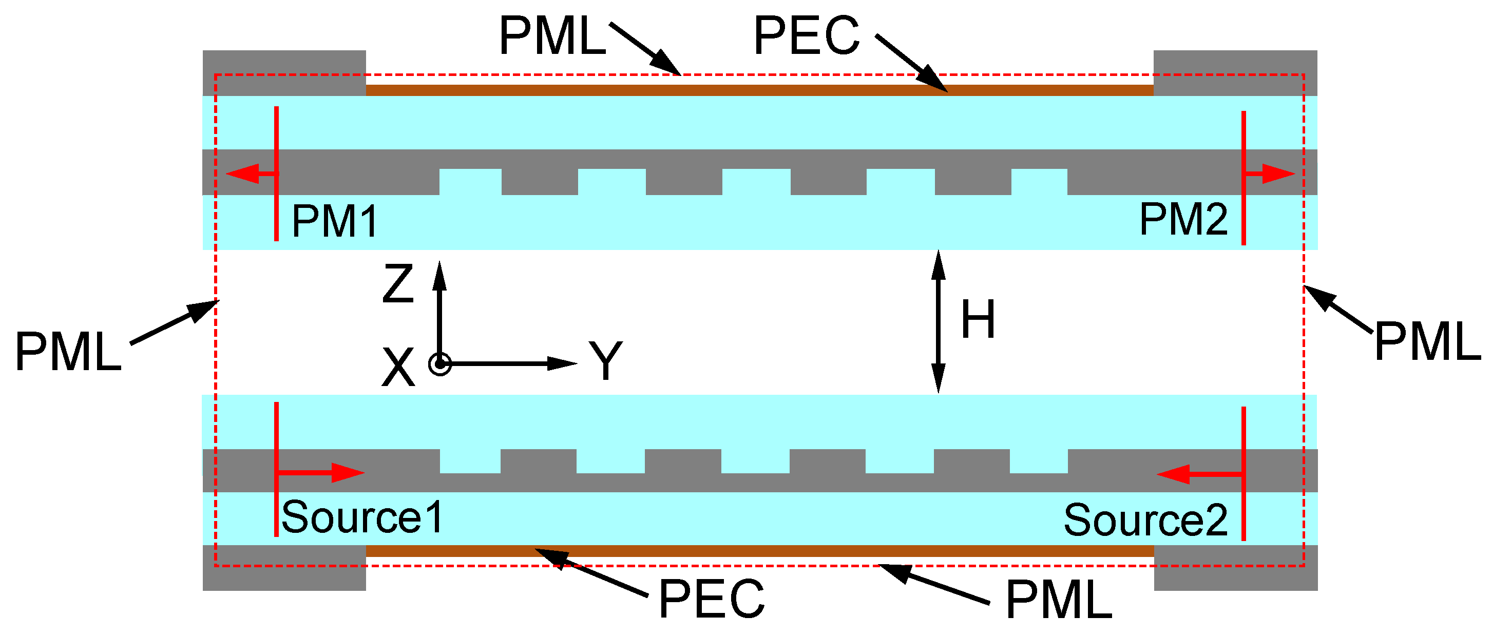
Figure 3, in our simulations, a rectangular simulation region was defined that encompasses the entire grating device (excluding the 3 dB splitter). The simulation region boundary was set as the Perfectly Matched Layer (PML) boundary condition to absorb light radiating to the surrounding environment. We model the metal mirror as a perfect electrical conductor (PEC). Then, two identical MSGC chips are aligned each other face to face with a vertical working distance (H) assumed to be 50 μm, which is a sufficient distance for most 3D stack packaging based on Cu μpillar bumps that has height of less than 50 μm. An index-matching material (such as UV glue A539-DM) with N = 1.56 is filled between the chips to minimize optical reflection. To minimize back-scattering and achieve a larger mode size, a shallow etch type with an etching depth of 70 nm is chosen. Other simulation parameters are listed in
Table 1. Due to the computational demands associated with the large simulation region, we primarily employ two-dimensional (2D) finite-difference time-domain (FDTD) simulations for our work, unless otherwise specified. It is important to note that, unless explicitly specified, all other simulation parameters were set to the default values provided by the software of Lumerical.
In 2D simulations, we cannot directly simulate the entire 3D structure, including the splitter and grating. Therefore, we emulate the coherent light from the 3 dB splitter by using two light sources with the same polarization mode (TE) and central wavelength (
Figure 3). In optical fiber communication, which commonly utilizes the C-band and L-band for efficient low-loss transmission at approximately 1310 nm and 1550 nm wavelengths, respectively. The central wavelength of 1550 nm is chosen to design a vertical grating coupler tailored for C-band applications. If the grating needs to be adapted for a different operating center wavelength, such as 1310 nm, the grating parameters can be adjusted accordingly to maintain optimal vertical coupling efficiency. The two mode sources with identical initial phase
and power
mW are injected into the bottom MSGC from the left and right waveguides. The optical phase and power from the waveguide ports (PM1 and PM2) of the upper MSGC are recorded. The total power output, denoted as
, from the 3 dB combiner of the upper MSGC is computed based optical coherent theory. The coupling efficiency is calculated as
. Firstly, a parametric sweep is performed to optimize the grating pitch and duty cycle. Two main objectives are considered in this optimization process: the first is reducing the grating reflection that returns to the input waveguide, while the second is ensuring phase matching between the upper radiated beam and the bottom reflected beam by the metal mirror.
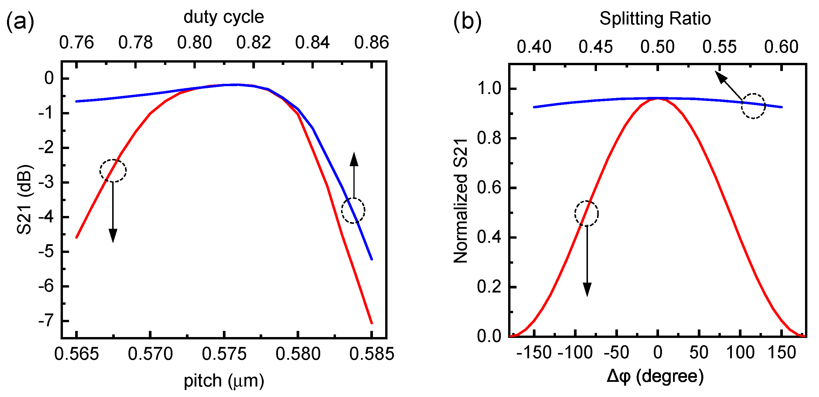
Figure 4a shows the optimized parameters.The minimum coupling loss achieved is 0.18 dB (96.0%) at a pitch of 0.575 μm and a duty cycle of 0.815 (etched length 106 nm). The corresponding fabrication tolerances at 1 dB are greater than ±5 nm and 0.075, respectively. In real applications, the splitting ratio of the beam splitter or combiner is rarely an ideal 1:1. Additionally, the lengths of the two waveguides connected to the grating are often not precisely equal, introducing a phase difference denoted as
between two input optical waves. Consequently, a comprehensive analysis is imperative to understand the impact of non-uniform splitting ratios and phase differences on the coupling efficiency. As shown in
Figure 4b, when the phase difference between the two input waveguides ranges from −180 degrees to 180 degrees, it causes a sharp transition in inter-chip coupling efficiency from 0 to 1. The phase tolerance at 1 dB is ±50 degrees. We further analyzed the influence of the splitting ratio of the splitter or combiner on coupling efficiency. When the imbalance of the splitter exceeds 1 dB, the coupling efficiency undergoes a 0.34 dB reduction (
Figure 4b). Based on the previous analysis, we deduced the optimal structural parameters for chip-to-chip MSGC, as summarized in
Table 1. The 1 dB fabrication tolerance of the MSGC is characterized by a pitch error of ±5 nm, a duty cycle error of 0.075, a waveguide phase imbalance of less than ±50 degrees, and a splitting ratio imbalance of >1 dB.
3. Optimal Coupler Performance
In this section, we investigate the optimized grating coupler performance, including the lateral alignment tolerance, height alignment tolerance, and wavelength bandwidth. As depicted in
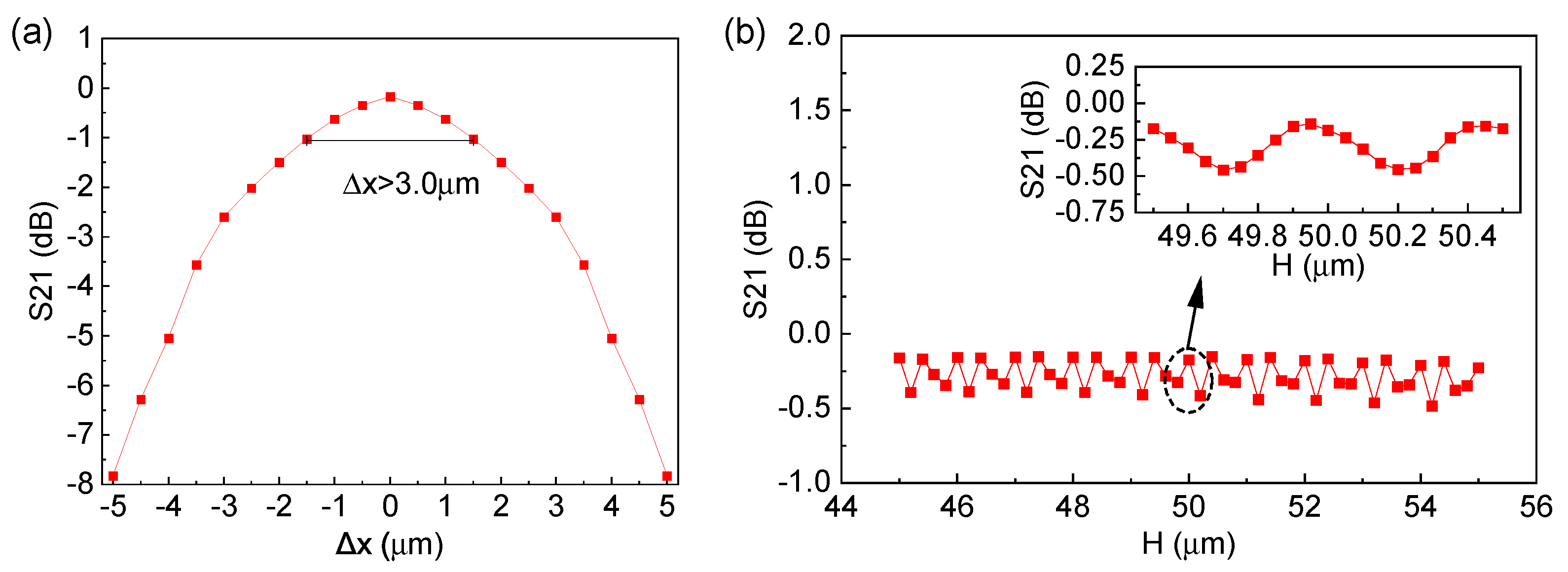
Figure 5a, our investigation initially focused on the impact of lateral misalignment along the Y−axis between the upper and lower gratings on coupling efficiency. With the alignment offset varying from
m to
m, a noticeable reduction in chip-to-chip coupling efficiency was observed, leading to a lateral alignment tolerance of
m at 1 dB. In practical three-dimensional stacking packaging processes, huge distance fluctuations between upper and lower chips are common. Consequently, an assessment of the influence of the vertical working distance becomes imperative.
Figure 5b illustrates that when the working distance fluctuates within
m around the center of
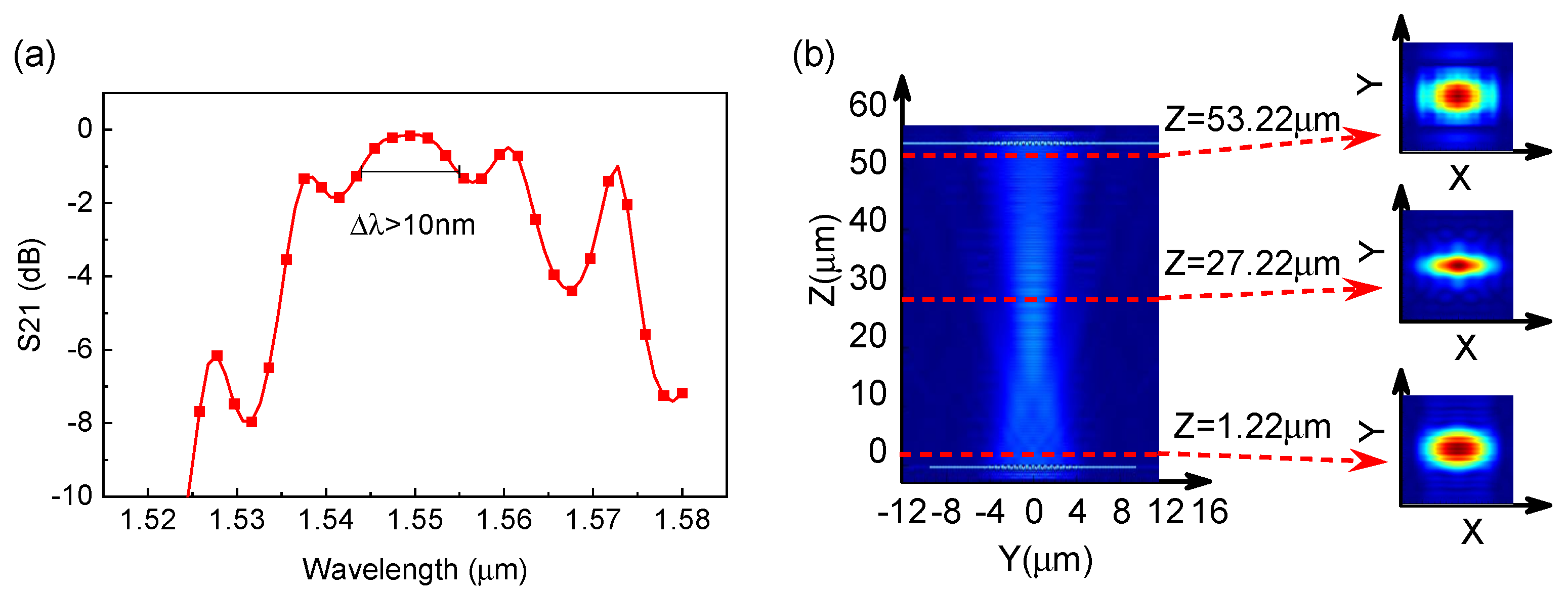
m, the associated grating coupling loss merely increases by a maximum of 0.5 dB. This result is mainly due to the high coupling efficiency between MSGC and free space, which effectively suppresses the reflection resonance between gratings. As a result, the coupling efficiency remains nearly constant regardless of the working distance. Additionally, we conducted an analysis of the spectral response, as illustrated in
Figure 6a. There are several peaks in coupling efficiency, which are mainly caused by grating reflection resonance. The grating exhibits a 1 dB wavelength spectral bandwidth of 10 nm. Finally, two same MSGCs with grating coupler lengths of 9
m, grating coupler widths of 14
m, and a working distance of 50
m are used in a 3D FDTD simulation to verify the effectiveness of our designed vertical coupler. Other simulation parameters are the same as listed in
Table 1. As shown in
Figure 6b, the optical field radiated from the bottom MSGC exhibits a Gaussian distribution and is received by the upper MSGC with a coupling efficiency of 87.2%. Our designed MSGC is compared with state-of-the-art couplers, as illustrated in
Table 2. It exhibits significant advantages in both working distance and coupling efficiency. Further optimization is needed to enhance the operating wavelength range. It should be noted that in the 2D simulation, the model assumes the grating coupler to be infinitely wide in the X−direction. Only the mode-field overlap coupling efficiency along the grating direction (Y) is considered, neglecting the influence of the grating coupler width in the X−direction on the coupling efficiency. Therefore, compared to the 2D simulation, the coupling efficiency in the 3D simulation is lower. To achieve better coupling efficiency, it would be necessary to analyze the effect of grating width on the coupling efficiency in 3D simulation mode. However, limited computational resources restrict our further investigation and analysis.


