1. Introduction
Surface plasmon polaritons (SPPs) are non-radiating surface electromagnetic waves guided by materials with negative permittivity [
1,
2]. The nature and properties of SPPs of the visible and mid-IR ranges, as well as their use for control of the surface and processes on it, have been studied quite well and have found wide application in optics [
3,
4], unlike SPPs of the terahertz (THz) range. The practical mastering of the THz range began only in the second half of the last century with the creation of laser sources (gas, free electron, semiconductor, and broadband pulsed) [
5] and sensitive detectors (thermal, photonic, pyroelectric, photoconductive antennas, etc.) of THz radiation [
6].
Calculations performed by the Drude model for the permittivity of metals show a very small difference between the THz SPPs and plane electromagnetic waves in the medium adjoining the metal. For example, on a flat homogeneous interface between a high-conductivity metal (Au, Ag, Cu, Al, and Pt) and vacuum (dry air), the calculated propagation length
L of THz SPPs is as large as tens and even hundreds of meters, and their phase and group velocities are less than the speed of light by only a few thousandths of a percent [
7,
8,
9].
Such properties of THz SPPs demonstrate their potential for use in communication devices (to increase the speed of signal transmission) and devices for optical information processing. However, the first experiments on the excitation of THz SPPs by laser radiation (
λ0 = 118.8 μm) have already shown that on the sputtered and polished surfaces of the abovementioned metals, the
L value does not exceed decimeters, i.e., is 2–3 orders of magnitude less than the calculated one, and the phase velocity differs from the speed of light not by a few thousandths, but by a few tenths of a percent [
7,
10,
11]. The main reasons for this were found to be (1) the presence of inhomogeneities and roughness on the surface (which leads to the appearance of radiative losses of SPPs) [
12,
13]; (2) the difference between the permittivity of the near-surface layer of the metal (skin layer) and that in the depth of the metal [
14]; (3) scattering of SPPs on the metal granules in the near-surface layer [
15]; and (4) incorrectness of application of the Drude model in the THz range because of the weakly anomalous skin effect when the mean free path of conduction electrons exceeds the depth of the skin layer (decreasing with increase in the radiation wavelength
λ0); thus, the electrons carry away energy deep into the metal, which is not taken into account by the classical electrodynamics [
16]. In addition, a certain contribution to the attenuation of SPPs is made by their thermal losses due to the skin effect and absorption of THz radiation by the water vapor in air.
Nevertheless, THz SPPs are effectively used for spectroscopy of subwavelength layers on a conducting surface when reflectometry methods are inefficient because of the high reflectivity of metals at THz frequencies [
17]. There are a number of publications on the use of THz SPPs in metal surface refractometry [
18,
19,
20], interferometry [
21,
22], semiconductor-heterostructure light emitters [
23,
24,
25], photodetectors [
26,
27], and sensor devices [
28,
29,
30], as well as in devices for control of THz SPP beams [
9,
31,
32]. In addition, it turned out that the propagation length of THz SPPs over a real metal surface (with roughness and impurities) can be made several times larger due to the application to it of a layer of a non-absorbing dielectric of a certain thickness (the presence of the layer leads to decrease in the radiative losses of SPPs and protects the metal from external influences) [
33].
According to most researchers in the field of THz plasmonics, one of the most topical problems is the conversion of the source radiation into SPPs. As known, for realization of this problem, it is necessary to fulfill the laws of conservation of energy and momentum for the bulk and surface waves. For the satisfaction of the first of the laws, the frequencies
ω of these waves must be equal and satisfy the condition
(where
is the plasma frequency of the metal). The momentum conservation law is satisfied when the tangential components of the wave vector of the radiation incident on the surface and the SPP wave vector are equal [
1,
2,
3]. While it is relatively easy to select a radiation source for a given metal, the wave vectors can be matched in only two ways: either by the method of attenuated total internal reflectance (ATR) or through the diffraction of the bulk wave on one or another inhomogeneity on the surface itself (planar diffraction grating, roughness, foreign inclusion, groove, etc.) or on an edge of an object placed in the medium (screen edge or prism edge) within the depth of penetration of the SPP field into it.
The ATR method is applicable if the SPP propagation length
L is comparable to or less than the radiation wavelength
λ0 and there is no necessity for the generation of SPPs with field distribution unperturbed by the coupling element. Therefore, the ATR method is used mainly in the visible range, in which the radiation frequency
ω for metals is slightly less than
[
34], which meets the abovementioned conditions. In the infrared and THz ranges, the radiation frequency is much lower than the plasma frequency of metals (
), and therefore SPPs are similar in their characteristics to a plane wave: the
L value is as large as thousands of
λ0, and the depth of field penetration into the medium is expressed in centimeters [
9]. Moreover, for large-wavelength SPPs, as well as for plane waves, the diffraction effects become more and more pronounced with increasing
λ0. Therefore, if the ATR method is used for the excitation of large-wavelength SPPs when the optical coupling of the SPPs and the prism on its edge is broken because of the diffraction of the SPP field on the edge, a high-power fan of parasitic bulk waves arises, which leads to large energy losses and unacceptably low efficiency of the conversion of the source radiation into SPPs on the prism-free surface of the metal.
Thus, for photon generation of terahertz SPPs on the surface of noble metals, only the phenomenon of diffraction is used and implemented with one or another technology.
The classical elements utilized for this purpose are planar diffraction gratings formed on the surface supporting the THz SPP propagation [
35,
36,
37]. To minimize radiative losses during the propagation of SPPs over the grating, the size of the grating (in the plane of incidence) must not exceed the diameter of the incident beam. Alternatively, the beam is directed to a grating portion adjacent to the flat surface of the sample under study (usually, the grating is deposited on a separate substrate adjacent to a flat face of the sample) [
38]. The presence of a dielectric coating of subwavelength thickness on the grating makes it possible to reduce SPP losses because of re-emission into the medium [
36]. The main advantage of grating coupling elements, in addition to their high efficiency, is their planarity, which enables the creation of compact devices. Their frequency and spatial selectivity in relation to the radiation to convert (applied in selective photodetectors [
39,
40]) is a limitation in the generation of broadband SPPs. The disadvantages of the grating method include the need to create a grating on the sample surface and significant diffraction losses during the transition of SPPs from the corrugated surface area to the plain one, which hinders the practical use of SPPs in the THz range.
Often, for excitation of IR and THz SPPs on a flat surface, the focused source radiation (monochromatic or broadband) is directed to the edge of a solid-state screen (aperture method) placed near the metal surface within the depth of the SPP field penetration into the medium (air) [
9,
41]. Diffracting on the edge, the incident radiation generates a set of plane waves the tangential components of the wave vector of which differ in the absolute value. Since the spectrum of the wave vectors of SPPs (even generated by monochromatic radiation) on a real surface has a certain width [
42]; some of the diffracted plane waves and components of the SPP spectrum satisfy the momentum conservation law, which leads to the excitation of SPPs. Of course, the efficiency of conversion of radiation into SPPs is low in this case (a few percent [
9,
41]). However, screen coupling elements are non-selective (neither in frequency nor in the angle of incidence of radiation), which enables their use for the generation of broadband SPPs by picosecond pulses [
43,
44] or by radiation from heat sources [
45]. Such elements have an obvious disadvantage of non-planarity and an advantage of contactlessness. Note also that in the so-called “two-prism” scheme for the measurement of the propagation length of IR and THz SPPs, the conversion of radiation into SPPs and vice versa occurs mainly due to the diffraction of the source radiation or the SPP field on an edge of the input or output prism, not due to ATR phenomena [
9,
46].
The method of diffraction of radiation on an edge (more rarely on a slot or groove) of the SPP support surface (the end-fire coupling technique) [
47] possesses the main advantages (planarity, ease of implementation, large bandwidth, contactlessness, and compactness of the coupling element) of the abovementioned technological methods of photon excitation of THz SPPs. The calculated value of the coupling efficiency by this method in the visible and near-IR ranges is as high as 80 ÷ 95% [
47,
48,
49]. The use of the end-fire coupling technique is possible at THz frequencies as well [
32,
50].
A common drawback of all the abovementioned methods for conversion of a bulk THz radiation into SPPs is the generation of intense parasitic bulk waves, both from the diffraction of the incident radiation and from the scattering of SPPs on surface roughness and optical inhomogeneities [
33]. Most of these waves are near-surface ones, and thus they create strong flare light to a photodetector placed near the surface of the sample under study. One of the simplest and most efficient methods of shielding from such flare light is the spatial separation of SPPs and parasitic bulk waves by coupling elements (for conversion both of the source radiation into SPPs and of SPPs into the bulk wave to detect) with a convex cylindrical surface capable of supporting SPPs [
51].
This article describes a technique for determination of the efficiency of SPP generation by the end-fire coupling method with the use of a coupling element in the form of a cylindrical segment, both in a “metal-vacuum” structure and in the presence of the metal of a non-absorbing dielectric layer of subwavelength thickness. Experiments on the approbation of the technique with the radiation (λ0 =141 μm) of the Novosibirsk free electron laser are described.
2. Theoretical Evaluation of the SPP Coupling Efficiency
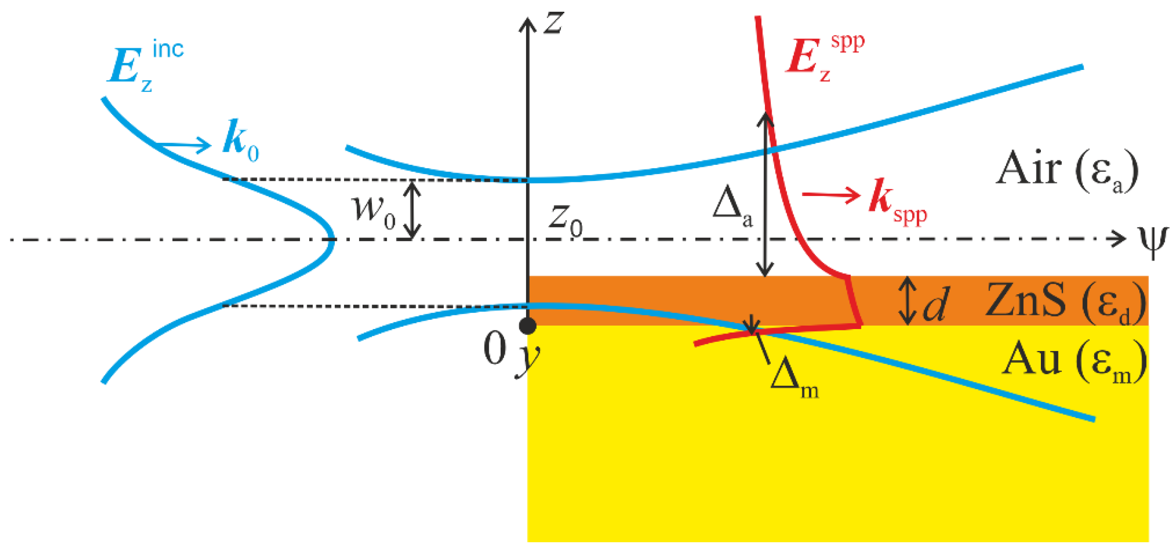
Let us consider a focused
p-polarized bulk wave with a Gaussian profile of the electric field vector
where
w0 is the waist of the beam and
k0 = 2π/λ
0 is the wavenumber of the source radiation incident along the
ψ axis on the rectangular edge of the conducting sample (
Figure 1); the center of the radiation beam is at the distance
z0 from the metalized surface of the sample. In our case, the surface is metalized by an opaque gold layer 300 nm thick, over which a zinc sulfide (ZnS) layer of thickness
d is deposited. The sample is in air with the dielectric permittivity
[
52].
Because of the diffraction of the incident wave on the edge of the sample, surface plasmon polaritons (SPPs) are excited in the Au-ZnS-air structure and propagate along it. The longitudinal component (along the
ψ axis) of the wave vector of the incident wave should be maximal (i.e., equal to
k0) to be as close as possible to the SPP wave vector
kspp. This is achieved in the region of the focused beam waist, where the beam wavefront is quasi-flat. In this case, the small difference between
k spp and
k0 (
) is compensated for at the diffraction of the radiation on the edge of the sample, which leads to the matching of the wave vectors of the incident and surface waves, which is necessary for the generation of SPPs. In this case, the efficiency of SPP generation depends mainly on the overlap (“matching”) of the fields
Ez (
z,y) of the incident and surface waves [
53].
Solving the wave equation for the three-layer structure (“Metal–Dielectric layer–Air”) subject to the boundary conditions for the tangential components of the magnetic (
Hyspp) and electric (
Exspp) fields gives the following solution for the
z component of the electric field vector of the SPPs
Ez (
z,
y) [
54]:
where
is the amplitude of the
z component of the SPP electric field;
,
, and
are the constants of the SPP field attenuation in the metal, dielectric, and air, respectively;
εm,
εd, and
εa are the permittivities of the respective media; and
is the complex refractive index of the SPPs.
Using reference experimental data for the wavelength
λ0 = 141 µm for ZnS (
, [
55]) and the effective permittivity of the deposited gold surface (
), identified within the SPP penetration into the metal [
56], we calculated the dependences of the depth of the SPP field penetration into metal
(
Figure 2a) and air
on the thickness
d of the ZnS coating (
Figure 2b) by numerical solution of SPP dispersion equation for three-layer structure. For comparison, the black lines in this figure show the similar dependences calculated for the permittivity
, found by the Drude model for crystalline gold [
57]. It can be seen that Δ
m for the deposited gold surface was five times larger than that for the crystalline metal and does not depend on the ZnS layer thickness. Δ
a for gold with the surface permittivity was noticeably smaller than that for the crystalline metal; moreover, for gold without the ZnS layer (
d = 0), this difference was almost one order of magnitude. These facts should be taken into account in the search for the optimal conditions for the generation of THz SPPs. Subsequently, all calculations were carried out with the effective permittivity of the deposited gold surface.
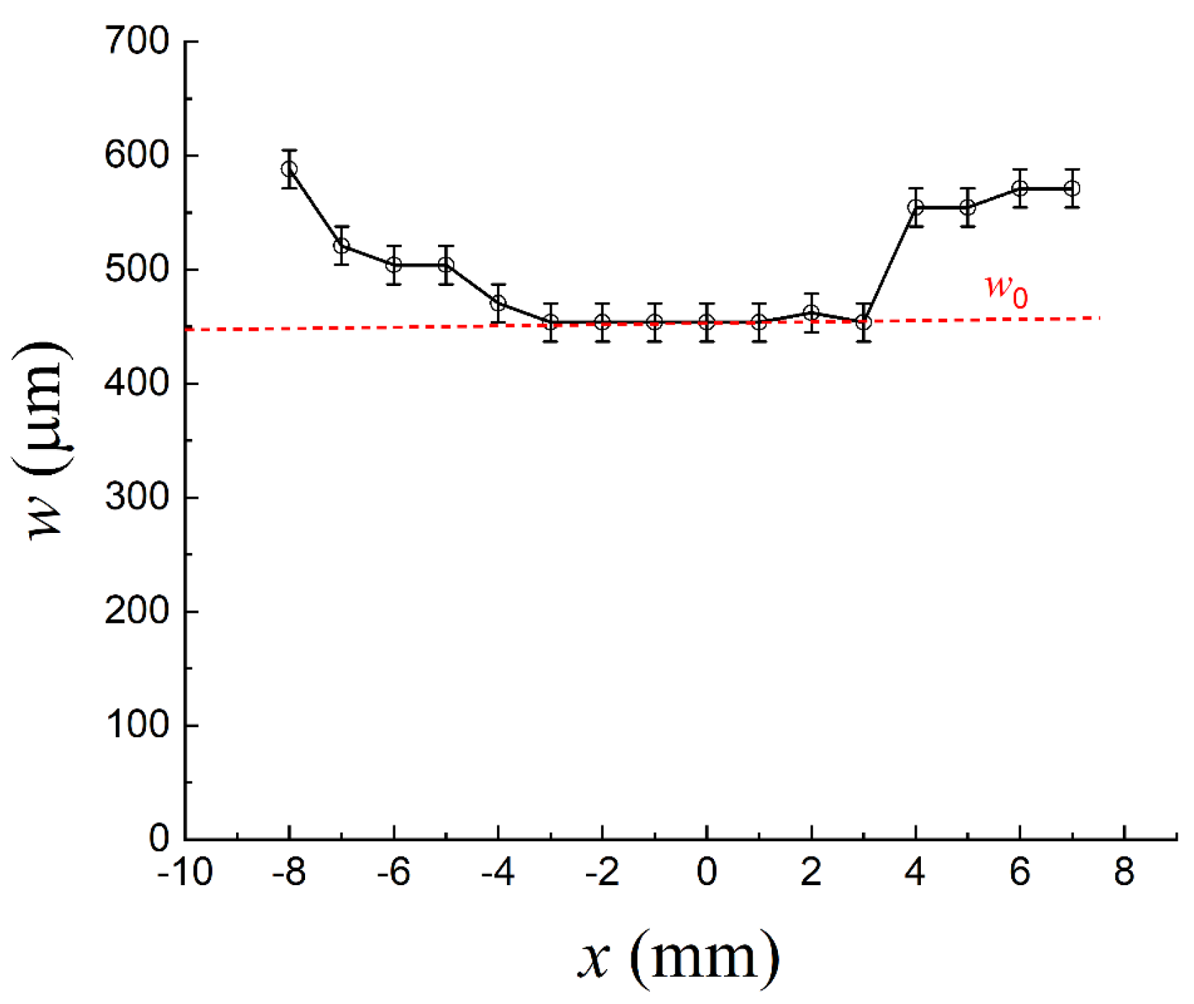
Using Formulas (1) and (2) and taking into account the normalization, we calculated the distributions of the incident radiation field
Ezinc (
z) (at
z0 = 0) with
w0 = 450 µm, found experimentally (see
Appendix A), and the surface wave field
Ezspp (
z) at different thicknesses of the ZnS coating (
Figure 3). As can be seen from
Figure 3a, the SPP field
Ezspp penetrates into the metal (
z < 0) to a very small depth (
≈ 250 nm), decreases a little in the dielectric (0 <
z <
d), and exponentially decays in the air (
z >
d) at a distance of the hundred micrometers (
Figure 3b).
Order of Several
At the transition of the metal–dielectric (
z = 0) and dielectric–air (
z =
d) interfaces, the field component E
zspp experiences a jump due to the concentration of the electric charge on the metal surface, which causes SPP propagation over the conductor surface [
54].
It can be seen in
Figure 3a that the field
Ez spp in the metal is several orders of magnitude smaller than the field in the dielectric layer or air, which indicates weak coupling of the SPPs with the metal surface and small Joule losses in the metal. With the increase in the thickness
d of the coating layer, the field
Ezspp in the air is confined to the surface of the sample (the depth Δ
a of penetration of the SPP field into the air decreases; see
Figure 2), and its intensity near the metal surface and inside the metal grows, which leads to increase in the Joule losses of the SPPs.
The efficiency of conversion of the incident wave energy into the surface wave energy is governed by the overlap (“matching”) of the fields of these waves, and, as can be seen from
Figure 3a,b, must strongly depend both on the coating thickness
d and on the value of
z0. When the beam center goes below the level of the metal surface (
z0 < 0), the coupling efficiency is expected to decrease, and with an increase in
z0 in the region of its positive values, it is expected to rise. To understand this in detail, we calculated the coupling efficiency
η of the incident bulk wave into SPPs using the classical expression [
58]
where the integration with respect to the
y coordinate yields unity because the profiles of the incident wave and the surface wave along the
y-axis coincide. The numerator of expression (3) contains the overlap integral of the fields of the incident wave and SPPs, and the denominator contains their intensity.
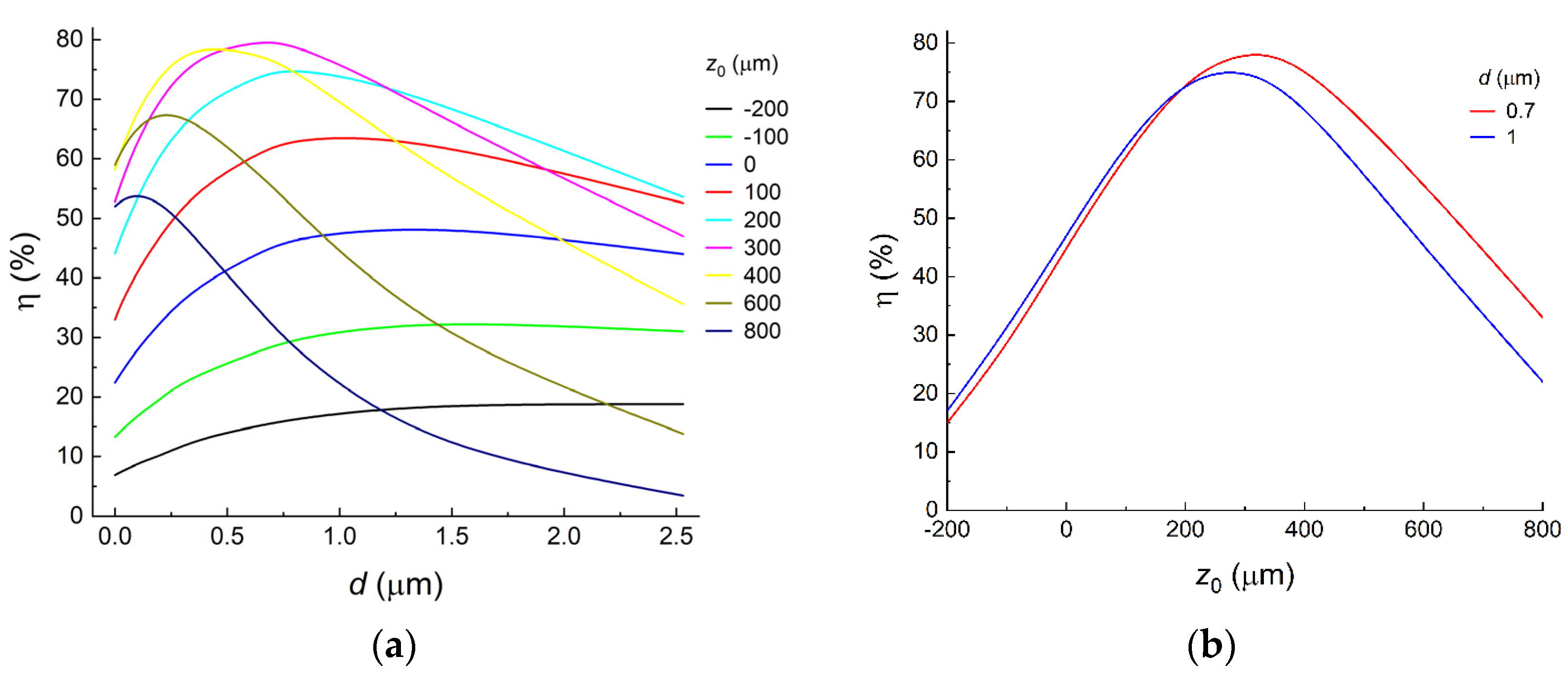
Using Expressions (1)–(3), we calculated the dependence of the SPP generation efficiency
η on the thickness
d of the ZnS coating for some positions
z0 of the central part of the incident beam in the range from −200 µm to 800 µm (
Figure 4a). With an increase in
d, almost all curves first showed growth of the
η value, which reached its maximum at a certain thickness
d of the ZnS layer and then gradually decreased.
Figure 4b shows the dependence of the efficiency on the position of the central part of the incident beam
η(
z0). Like the dependence
η(
d),
η(
z0) had a maximum, but at a certain
z0. Thus, it can be stated that there is an optimal thickness
d of the coating layer and a position
z0 of the incident beam at which the efficiency of the conversion of the incident wave into SPPs will be the highest, which is due to the maximum overlap of the fields of the bulk and surface waves (see
Figure 3b).
According to
Figure 4, the maximum efficiency of THz SPP generation in the example under consideration is
η ≈ 80%, which is comparable to the maximum achieved efficiency in the visible and IR ranges (80–95%, [
47,
48,
49,
50]). The efficiency of SPP generation can be raised even more if the incident wave profile shape is made as close as possible to the SPP field distribution. Among the available works on the evaluation of the efficiency of generation of SPPs by the end-fire coupling technique in the THz range, the highest calculated efficiency on bare metal with a dielectric waveguide as a coupling element was about 46% [
59]. Note that the abovementioned estimate of the SPP coupling efficiency was obtained under the condition of approximate equality of the wave vectors,
. With increase in the thickness of the coating layer, the difference between the vectors
and
becomes significant, which leads to the growth of the energy losses of the incident wave in the scattering on the edge of the sample and a corresponding decrease in the efficiency of SPP generation. In addition, in our calculations, it was assumed that the edge of the sample had an ideally rectangular shape, as well as even and smooth boundaries. The presence of irregularities on the edge and surface of real samples leads to additional growth of the diffraction energy loss of the incident wave [
53].
3. Experimental Setup
One of the main difficulties in experimental evaluation of the efficiency of conversion of focused radiation into SPPs by the end-fire coupling technique on flat conducting surfaces is the presence of parasitic bulk waves, which inevitably arise because of both the diffraction on the edge of the sample and the radiative losses of SPPs on surface inhomogeneities. These bulk waves make a significant contribution to the detected signal, which distorts the measurement results. However, if samples with a convex surface are used, then both types of parasitic bulk waves can be spatially separated from SPPs, and the efficiency of SPP generation can be estimated more correctly. For this reason, in this work, we used samples with a cylindrical conductive surface, which were earlier studied in [
51].
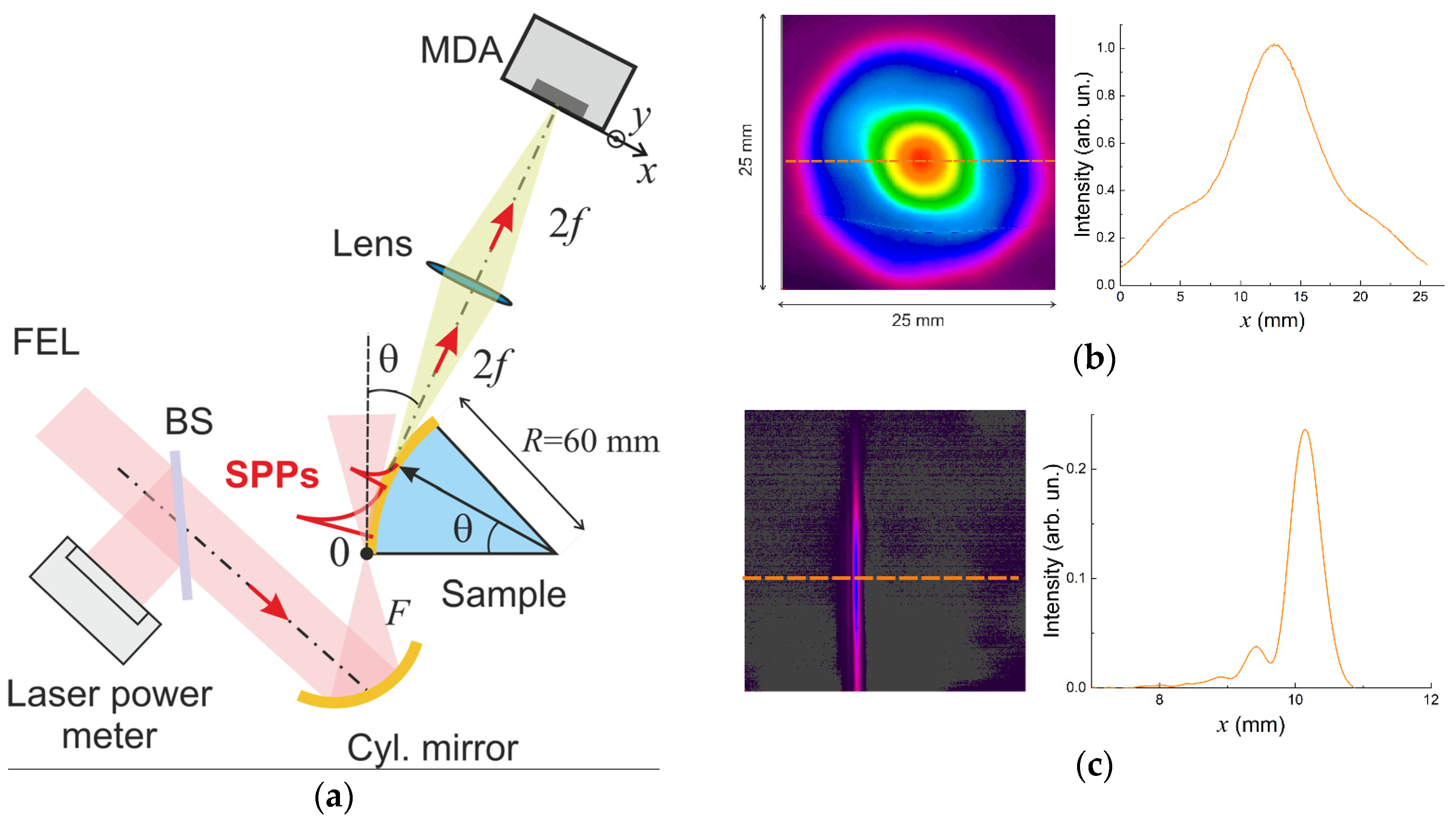
The scheme of the experiment is shown in
Figure 5a. The terahertz Gaussian beam (
Figure 5b) of the Novosibirsk free electron laser (NonoFEL) with a beam waist of 11 mm and wavelength
λ0 = 141 μm was focused by a cylindrical mirror (
F = 80 mm) on the edge of the cylindrical face of the sample, where part of the radiation energy was converted into SPPs because of diffraction. For achievement of the maximum efficiency of the SPP generation, the optical axis of the focused beam (according to
Section 2) was directed tangentially to the surface of the cylinder at the generation site (
θ = 0), and the point of incidence of the beam was adjusted along the
z-axis so that the intensity of the generated SPPs was maximal at a certain position
z0 of the center of the incident Gaussian beam with respect to the sample surface. The sample was one-eighth of a glass cylinder with a radius of 60 mm. Its optically polished convex surface has a coating of a magnetron-sputtered opaque layer of gold 0.3 µm thick, over which a uniform layer of zinc sulfide (ZnS) of some thickness
d in the range from 0 to 2 µm was deposited in a single technological cycle by electron beam sputtering. The thicknesses of the ZnS coatings were measured at several points along the cylindrical samples with the “Spektr” ellipsometer, developed by the Institute of Semiconductor Physics SB RAS [
60].
Because of the curvature of the sample surface, the SPPs supported by it were converted with some efficiency into bulk waves, emitted tangentially to the surface into the surrounding space. This bulk radiation from the SPP track was detected with an imaging system consisting of a silicon (HRFZ) lens with focal length
f = 75 mm and microbolometer detector array (MDA) [
61,
62], which were placed according to the 2
f-2
f scheme. The MDA contained 320 × 240 microbolometers, each of 51 μm in size (the size of the array was 16 × 12 mm
2). The angular distribution of the SPP intensity was recorded with a variation of the observation angle
θ of the bulk waves breaking off the SPP track (the angle
θ corresponded to the angular coordinate of the SPP break-off point). For recording the intensity distribution in cross sections of higher-power incident and focused beams (
Figure 5b,c), we used the pyroelectric detector array Pyrocam IV (Ophir photonics), which is less sensitive to THz radiation and has a larger size of 25 × 25 mm
2 (320 × 320 pixels). In addition, unlike the MDA, the Pyrocam detector does not have an input window, which makes it possible to avoid multiple interference in it. For control of the NovoFEL power at the input of the setup, part of the radiation was reflected from the beam splitter
BS and recorded by the laser power meter.
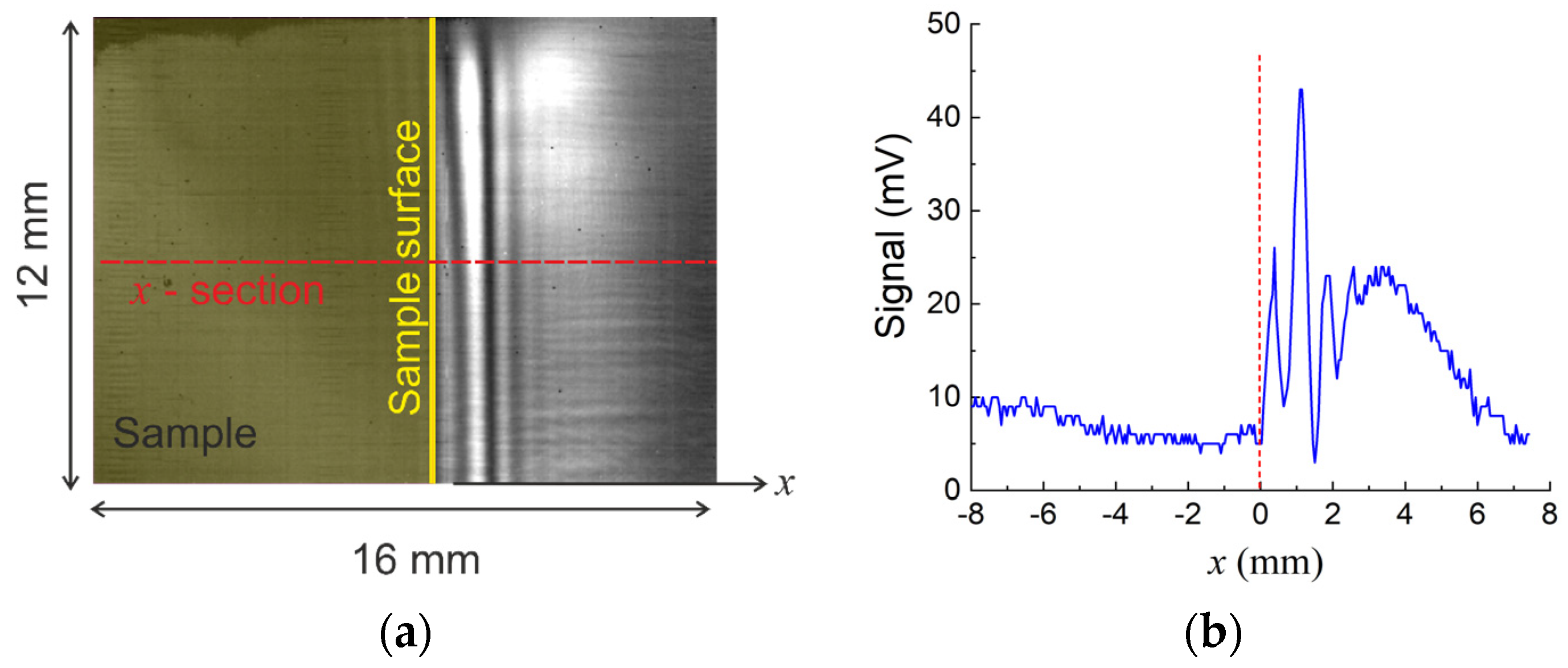
Figure 6a shows an example of the intensity distribution in the cross-section of the beam of bulk waves breaking off the SPP track on a sample with a ZnS coating 0.75 μm thick at the observation angle
θ = 27°, obtained with the imaging system.
Figure 6b shows the profile of a cross-section of this distribution along the
x-axis. The position of the sample surface corresponds to
x = 0. On the right-hand side from the sample surface (
x > 0), the signal has a complex profile of a series of maxima and minima, which turns into a gradual decrease in intensity. Such a pattern is associated with the interference of coherent waves breaking off the nearby portions of the SPP track, as well as with the multiple interferences in the germanium window of the detector array. Note that the bulk waves arising at the diffraction of the laser radiation incident on the sample edge could not get into the detector because at
θ > 13° the detector was reliably shielded from them by the convex surface of the sample.
Geometric estimates (see
Appendix B) showed that the range of angles of incidence of bulk waves breaking off the SPP track onto the detector array is governed by the lens diameter
D = 50 mm; it was
, which corresponded to the cylindrical surface segment
. In this case, the radiation incident on the detector array illuminated only half of its detection area, and thus the total power
of the radiation breaking off the segment Δ
l could be found via integration of the signal over all illuminated pixels of the detector.
4. Experimental Results and Analysis
According to the law of energy conservation, in the absence of non-linear interaction of the SPP field with the sample surface (which was so at the radiation power densities used in the experiments), the intensity of SPP radiation losses
Irad due to the curvature of the surface at a given angle
θ of their detection is proportional to the energy of the surface wave,
. Therefore, the rate of attenuation of the SPP intensity is equal to the rate of attenuation of the recorded signal:
where
α is the coefficient of SPP attenuation during the SPP propagation over the cylindrical surface, and
can be found from the measured dependence
.
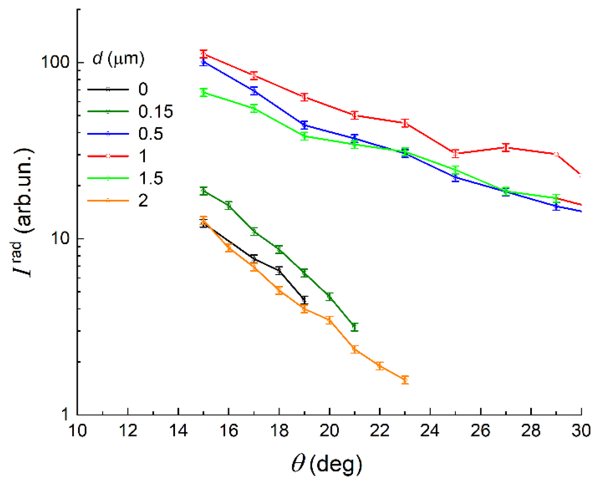
Figure 7 shows the dependences
measured with the detector array for samples with different thicknesses of the ZnS coating layer. The slope of the graphs is governed by the coefficient
α. Approximating these dependencies with an exponential function of the form
where
is the path the SPPs propagate from the place of their generation (the edge of the convex surface of the sample) to the observation point, at which we found the coefficient
α. The coefficient
A at the exponent corresponded to the intensity of radiative losses at
θ = 00 and
I0 related to the background noise.
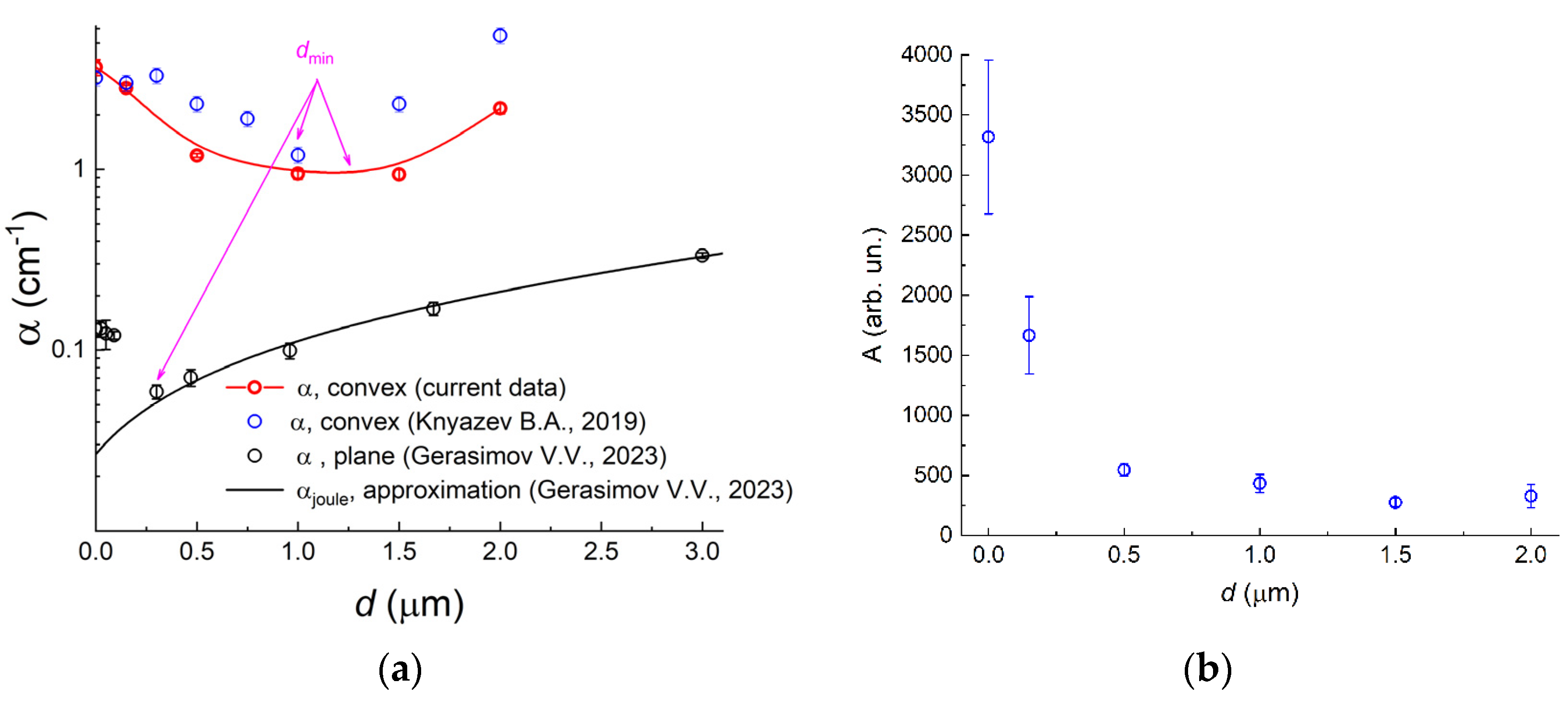
The red circles in
Figure 8a indicate the experimental values of
α resulting from the approximation for different thicknesses
d of the ZnS coating, and the blue circles in
Figure 8b show the corresponding values of the coefficient
A. For comparison, the blue dots in the graph (
Figure 8a) show data from the previous experiments on the study of SPP propagation over cylindrical surfaces, performed with a lens-Golay cell imaging system (with a narrow slit at the entry) with its elements placed according to the 2
f-2
f scheme [
51]. In that case, the samples were one-fourth parts of cylinders of the same radius
R = 60 mm, their convex surface metalized with gold, in which the thickness of the ZnS coating was significantly inhomogeneous along the SPP track (because of shortcomings in the ZnS sputtering technology on the cylindrical surfaces), which led to additional radiative losses of SPPs. According to ellipsometric measurements, in the samples used in this work (segments of identical cylinders with an angle of 45° at the apex), the thickness uniformity of the ZnS layer was much better, as evidenced by the lower values of
α (
Figure 8a), especially so at
d > 1.0 μm.
The experimental dependences
α(
d) presented in
Figure 8a have minima, which are due to the competition between two types of SPP losses during the SPP propagation over the convex surface: (1) ohmic losses
αjoule in the metal and (2) radiative losses
αrad arising both from the curvature of the surface and from surface inhomogeneities [
33,
51]. The total losses of SPPs are equal to the sum of these two types of losses:
On the one hand, as
d increased, the ohmic losses rose because the surface wave energy fraction transferred in the metal was higher in the presence of a dielectric coating layer on the metal (see
Figure 3a). On the other hand, as
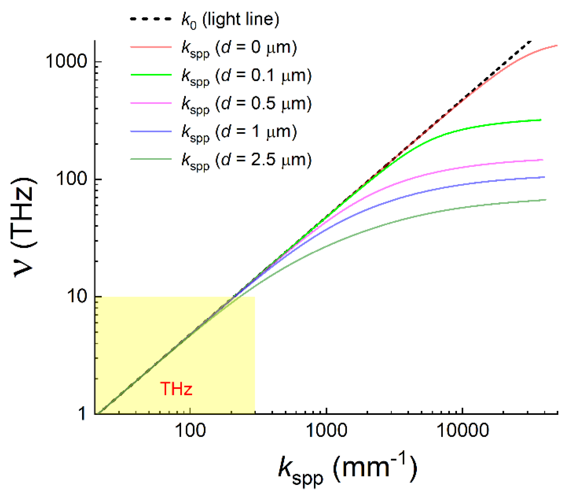
d increased, the radiative losses of SPPs decreased because the application of the dielectric layer to the metal leads, due to the higher SPP wave number
, to a larger distance between the SPP dispersion curve from the light line in the graph of
(see
Appendix C) and, consequently, to a lower probability of conversion of SPPs into bulk waves on the curvature and inhomogeneities of the surface [
33]. Therefore, at a certain coating thickness
dmin, the total losses of SPPs
α reached the minimum.
Figure 8a shows that the minimum on the curve
α(
d) for the samples used in this work was reached at
dmin ≈ (1.0–1.5) µm when the SPP attenuation coefficient
α decreased by a factor of 4 compared with the case of gold surface without a coating.
For assessment of the ratio of the SPP losses during SPP propagation over flat and cylindrical surfaces (with
R = 60 mm), the black dots in
Figure 8a show the
α(
d) values obtained in experiments on gold surface refractometry [
56]; the gold was deposited by the same technology on a polished flat glass surface. It can be seen that for the flat surface, the coefficient
α was approximately an order of magnitude smaller than that for the cylindrical surface, which indicates the predominance of radiative losses on the curvature of the surface over the losses on the plane, the latter consisting of the ohmic losses in the metal and radiative losses on surface inhomogeneities. Note that for the flat surface, there was also a minimum of total SPP losses, but at a smaller thickness of the ZnS layer (
dmin ≈ 0.3 μm) as compared with the cylindrical surface, which is due to the absence of radiative losses on the curvature.
The black solid curve in
Figure 8a shows the dependence of the ohmic loss coefficient in the metal
αjoule (
d), found by approximation of the experimental dependence in [
56]. These
αjoule(
d) values corresponded to the effective permittivity of the sputtered gold surface
εm = −7000 +
i·3000, which was approximately two orders of magnitude less than the crystalline metal permittivity calculated by the Drude model for
λ0 = 141 μm (
εDrude = −104700 +
i·317180). It can be seen that at
d ≈ 0 μm, the ohmic losses
αjoule of SPPs in the metal were an order of magnitude less than the radiative losses of SPPs on the flat gold surface without coating and approximately two orders of magnitude less than the total losses of SPPs on the metalized cylindrical surface.
From the graph in
Figure 8b it can be seen that the coefficient
A, which characterizes the radiative losses of SPPs at
θ = 0, had the greatest value at
d = 0, which is explained by the weak coupling of the SPPs with the bare metal (the depth of penetration of the SPP field into the air at
d = 0 is maximal (see
Figure 3b), and on the graph of
, the SPP dispersion curve came closest to the light line (
Appendix C). As
d increased, the radiative losses gradually decreased, which indicates improvement in the optical coupling of the SPPs with the sample surface (the SPP field is localized near the surface, and the SPP dispersion curve moves away from the light line).
5. Experimental Evaluation of SPP Coupling Efficiency
As SPPs propagate over the cylindrical surface, their intensity weakens as follows:
where
is the SPP intensity at the place of SPP generation at
θ = 0 (the values of the angle
θ are in radians).
With Expressions (4) and (7), the attenuation rate of the intensity of the radiative losses recorded by the imaging system can be written in the following form:
Integrating expression (8) over the observation angle of the detector array, i.e., from
to
(where
, see
Appendix B), we obtain
According to (5), the coefficient at the exponent
. Therefore, one can find the intensity of SPPs at the place of SPP generation on the edge of the sample (for
θ = 0):
Then the coupling efficiency of SPPs can be determined as
where
I0 is the intensity of the radiation incident on the edge of the sample. The value
(r. u.) was found by integration over the focal spot region recorded with the imaging system containing the MDA (see
Figure 5a).
Figure 9 shows the
η(
d) plot determined in this way. On the bare gold, the SPP coupling efficiency was
η ≈ 20%. With a ZnS layer deposited on the gold surface, the SPP generation efficiency increased, reached the maximum (
ηmax ≈ 60%) at
d ≈ 1 μm, and then gradually decreased. For comparison, this figure shows the theoretical dependences
η (
d) calculated by Formulas (1)–(3) (see
Figure 4a) for two values of
z0 (position of the central part of the incident beam with respect to the metal surface), which are in the best agreement with the experiment. It can be seen that at the ZnS layer thickness 0 <
d < 1 μm, there was good agreement between the experiment and theoretical estimates, and at
d > 1 μm, the decrease in the experimental values of
η was noticeably greater than that in theory. As noted in
Section 2, the decrease in the coupling efficiency of SPPs at large thicknesses of the dielectric coating can be caused by the larger difference between the SPP wave vector
and the wave vector of the flat wave
. This hinders the fulfillment of the condition of their matching, which leads to larger energy losses of the incident wave at diffraction on the sample edge. In addition, an increase in the diffraction losses can also be caused by the imperfection of the sample edge (its roundness and divergence from a straight line [
53]).
According to the calculations (see
Figure 4), the maximum of the dependence
η (
d) is reached at a slightly thinner ZnS layer (
d ≈ 0.7 μm) when the efficiency is close to 80% (20% higher than that in the experiment). This difference can be caused both by alignment inaccuracy in the search for the optimal position
z0 and by less probability of matching of the wave vectors of the incident wave and SPPs because of imperfection of the edge sample.

 ,
, 


