Article

A Novel PWM Signal-Generation Strategy for Pockels Cell Drivers

1
Anhui Institute of Optics and Fine Mechanics, Hefei Institutes of Physical Science, Chinese Academy of Sciences, Hefei 230031, China
2
Science Island Branch, Graduate School, University of Science and Technology of China, Hefei 230026, China
3
Jiangsu Provincial Sensor Network Engineering Technology Research Center, Wuxi Institute of Technology, Wuxi 214121, China
*
Author to whom correspondence should be addressed.
Photonics 2023, 10(8), 866; https://doi.org/10.3390/photonics10080866
Submission received: 26 June 2023 / Revised: 22 July 2023 / Accepted: 24 July 2023 / Published: 26 July 2023

Abstract

:
A Pockels cell driver (PCD) can be viewed as a high-voltage pulse width generator for controlling the bi-refringence effect of electro-optical crystals. The main features of a PCD include a high repetition rate, fast on and off switching, variable pulse duration, and a true square pulse shape. The most commonly used PCD has a narrow pulse width tuning range, typically within a few microseconds. In this paper, we propose a PCD based on a novel pulse width modulation (PWM) signal-generation strategy that can continuously adjust its pulse width with a minimum step size of 10 ns and no restriction on the maximum width. Therefore, it is easily compatible with both “On-type” and “Off-type” applications of the electro-optic crystal quarter-wave voltage. The experimental results show that the rising and falling times of the proposed PCD are approximately 7.3 ns and 7.8 ns, respectively, with a maximum repetition rate of 1 MHz and a maximum voltage of approximately 2.0 kV. Finally, the functionality of the PCD is demonstrated in a home-built slab laser.

1. Introduction

1.1. Description of a PCD

A PCD is a high-voltage pulsed power modulator used to control the bi-refringence of an electro-optical crystal (such as KTP, KD*P, or BBO) in order to drive the polarization direction of the light propagating through the crystal. They are widely used for Q-switching [1,2,3], pulse picking [4,5], cavity damping [6,7] and regenerative amplifier control [8,9,10,11]. Taking Q-switching as an example, Figure 1 shows the optical arrangement of a solid-state laser in two different operating modes [12]. As the arrangement in Figure 1a shows, the PCD uses quarter-wave “Off-type” voltage to keep the resonator closed, and then the voltage switches down to zero and the resonator is opened. On the contrary, the arrangement shown in Figure 1b uses a zero level of control voltage to provide the closed condition of a laser cavity. The resonator is opened by applying a quarter-wave voltage to the electro-optic crystal (called “On-type” voltage). The duty cycle of the high-voltage pulses generated by the PCD varies from application to application. It is difficult for a single product to meet different application requirements, especially to achieve high-precision wide-range pulse width adjustment and to meet a variety of compatibility applications for “On-type” and “Off-type” operations. In this study, we apply a novel PWM signal-generation strategy to the PCD design to address the aforementioned issues.

1.2. Major Factors Affecting PCD Performance

In the past, the majority of the research conducted on PCDs has focused on switching components and topologies, but the control methods, which are extremely significant, have rarely been discussed. We discuss these major factors affecting PCD performance in the following sections.

1.2.1. Switching Components

The characteristics of the switching components are the main factors that determine the performance of a PCD. High-voltage vacuum tubes, such as krytron and thyratron [13,14], were used in the early days; these components can generate pulses with nanosecond rising/falling times, but the repetition frequency is not optimal, and the device is bulky and complex.
The second method uses a bipolar transistor in series [15,16], in order to improve the operating voltage; however, the circuit is complex and the reliability is poor when extreme voltage is required. A nanosecond rising/falling time can also be obtained in this approach. When Marx-configured avalanche transistor circuits [17,18,19] are used, sub-nanosecond edge time can be obtained, but the repetition frequency is low.
A third method is to use metal-oxide semiconductor-field-effect transistors (MOSFET) [20,21,22] or silicon carbide (SiC) MOSFETs [23,24], due to their high breakdown voltage (upper kilovolt), several nanosecond edge time, high repetition rate, and low cost. The performance among the various switching components is presented in Table 1.
Vacuum tubes are scarcely used today, avalanche transistors can be used to generate sub-nanosecond rising/falling times, and SiC MOSFETs are widely used to generate nanosecond rising/falling times and high repetition rates.

1.2.2. Selection of Topology

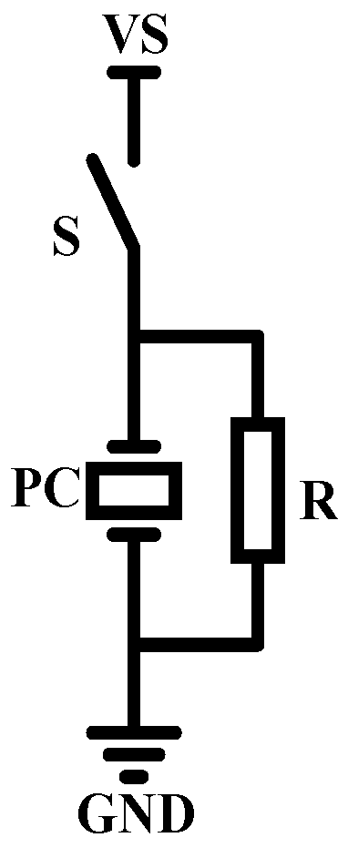
Common PCD topologies include the single switch type, the push-pull type, and the full-bridge type. The single switch type is the simplest structure, but Pockels cell voltage recovery relies on RC discharges, which take a long time and are not suitable for Q-switching with high repetition rates [25]. The structure is shown in Figure 2, where VS is the quarter-wave voltage of the Pockels cell (PC).
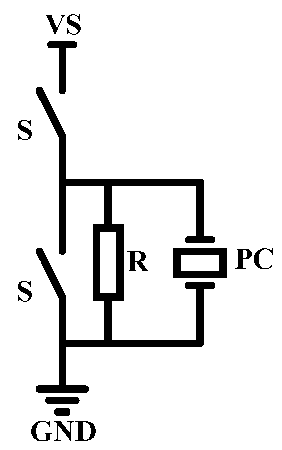
In the push-pull type shown in Figure 3, one side of the PC is connected to a push-pull circuit, and the remaining side is pulled to GND. In this way, the PC can be rapidly recharged and discharged by the push-pull circuit, enabling extremely high switching frequencies [26,27,28,29].
Figure 4 shows the full-bridge structure with two different power supply modes. The circuits in Figure 4a,b use unipolar and bipolar power supply and can generate unipolar and bipolar voltages, respectively. Clearly, a bipolar supply with half the voltage of a unipolar supply can lessen the stress on insulation and reduce the chances of arcing over to ground.

1.2.3. Control Method

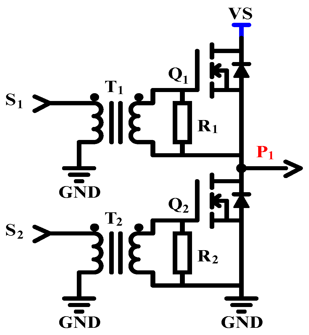
Currently, a push-pull circuit using MOSFETs as the high-voltage switching elements and isolated from the low-voltage control signals S 1 and S 2 by a transformer is commonly used, as shown in Figure 5.
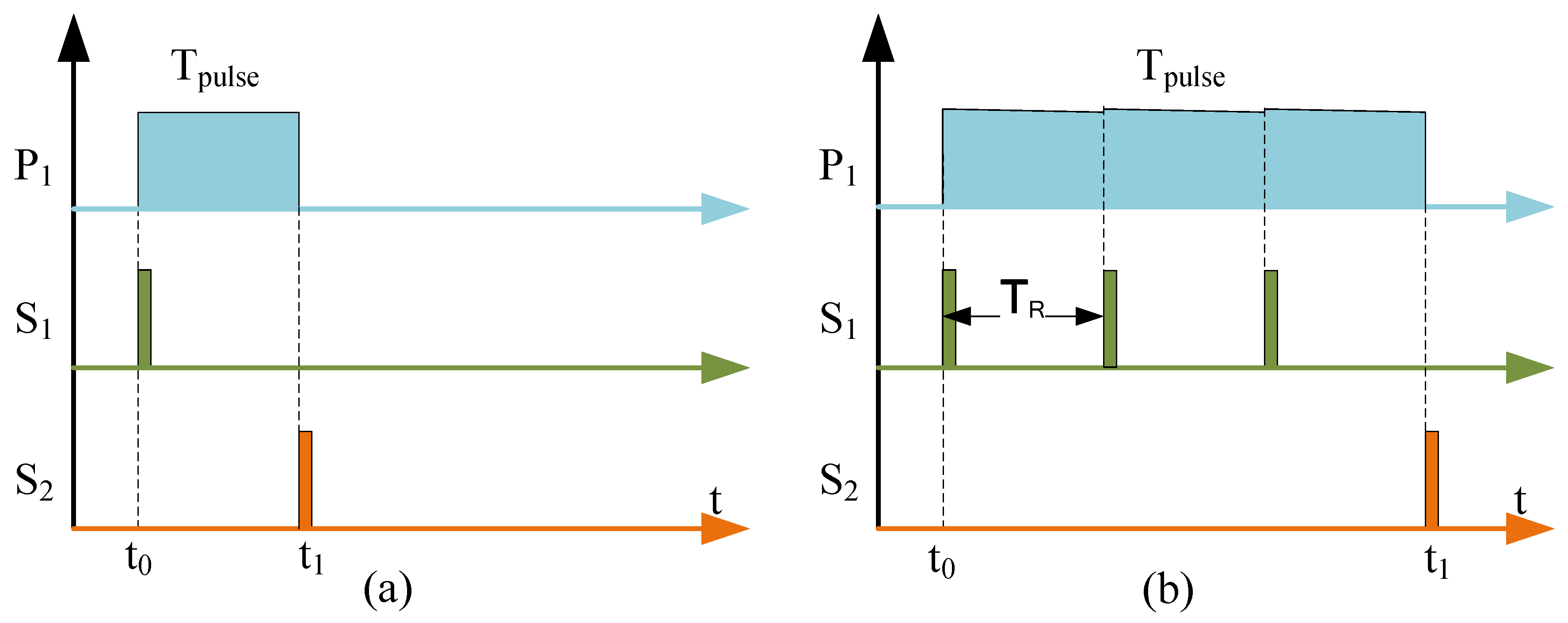
In order to generate positive pulses of width T p u l s e , it is common practice to drive the upper and lower bridge arms alternately with a time interval of T p u l s e . The resulting sequential waveform is shown in Figure 6a. This control method has two drawbacks:
(1)
The on-time lengths of Q 1 and Q 2 following the drive signals S 1 and S 2 are limited to prevent core saturation, which is due to the volt-second product of the gate drive transformers, and this time length is normally on the order of microseconds. When P 1 generates a high voltage with Q 1 switched on, it gradually decreases due to the leakage current, which limits the maximum width T p u l s e that can be achieved. In this paper, we propose a recharging method to extend the pulse width. Although this method produces a certain amount of ripple, it can be reduced to a negligible degree by increasing the repetition rate, as shown in Figure 6b.
(2)
In addition, a dead time T d e a d must be introduced to prevent the upper and lower bridge arms from conducting simultaneously, as shown in Figure 7. For fast MOSFET switching, it is safe to set a dead time interval of at least a few tens of nanoseconds, in which case the minimum width that T p u l s e can achieve is represented by Equation (1).
T p u l s e = T p u s h + T d e a d
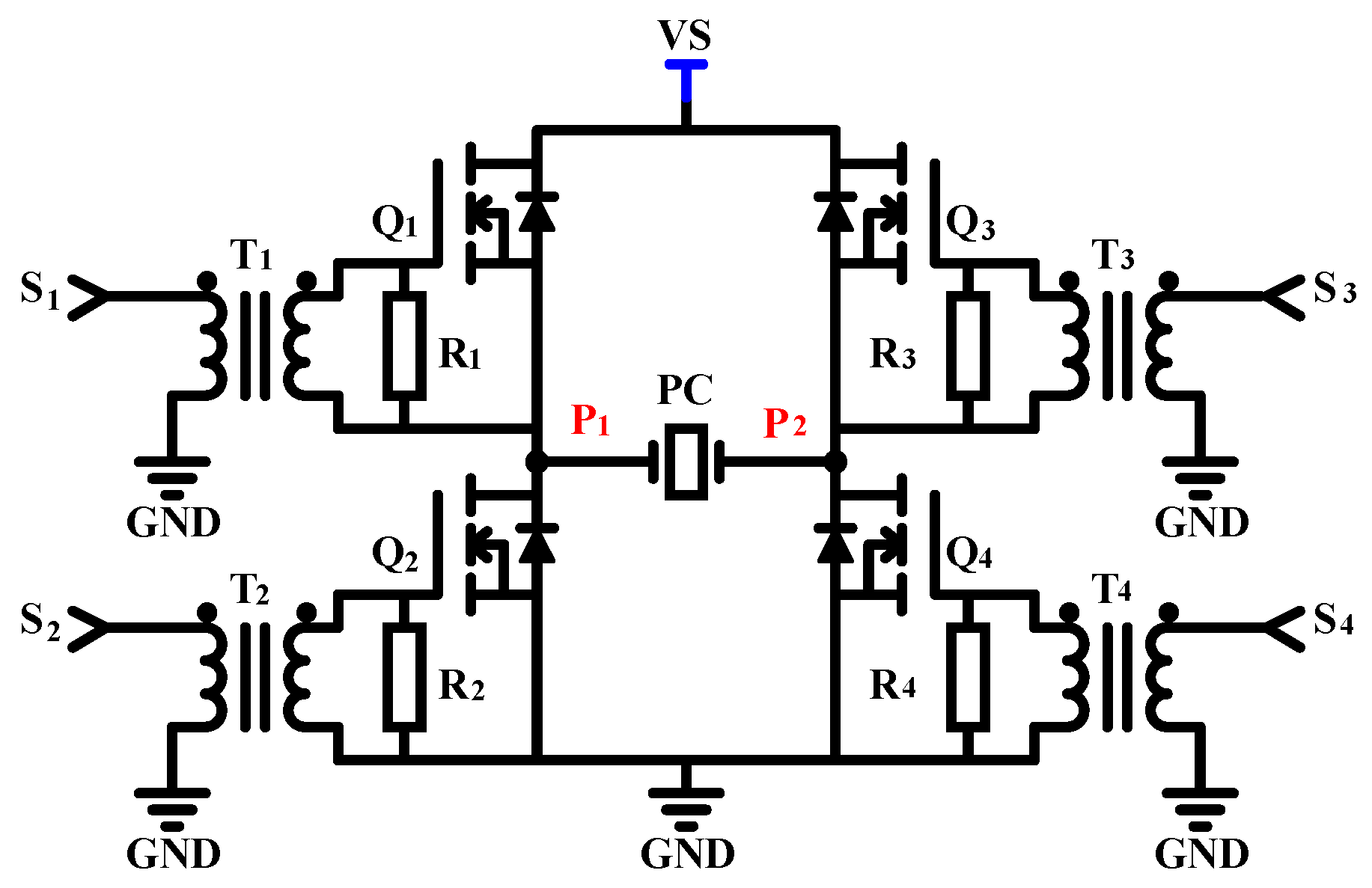
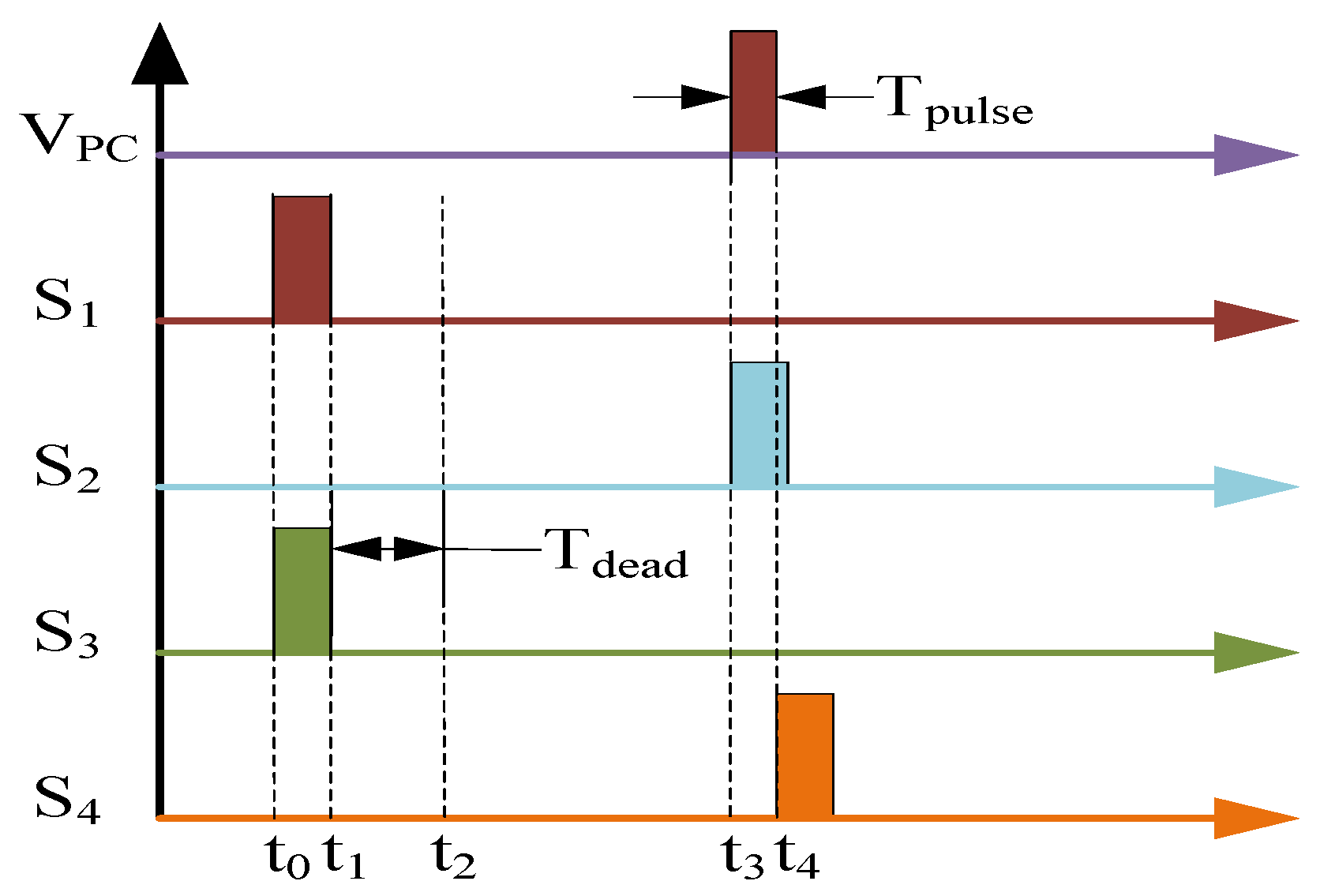
The effect of dead time can be eliminated by using the full-bridge circuit shown in Figure 8 and the timing control method shown in Figure 9. At time t 0 , S 1 and S 3 generate positive pulses, Q 1 and Q 3 are switched on, and the P 1 and P 2 are VS with zero V P C . Assuming that T d e a d = t 2 t 1 , the safety time reserved at t 3 is greater than the dead time; S 2 generates a positive pulse, Q 2 is switched on, and V P C is VS. Then, at time t 4 , S 4 generates a positive pulse, Q 4 is switched on, and V P C is zero. Since the time interval between t 3 and t 4 can be extremely short without dead time constraints, a narrow pulse of width T p u l s e = t 4 t 3 can be generated.

1.3. Introduction of the Proposed PCD with a PWM Signal-Generation Strategy

We propose a novel high-voltage PWM signal-generation strategy and design a PCD with continuously tunable pulse width using the previously mentioned modified push-pull circuit timing control method. This PCD can be applied to Q-switched lasers, pulse pickers, regenerative amplifiers, and other applications by tuning the high-voltage pulse width.

1.3.1. Generation of High-Voltage PWM Signals with Full-Bridge Topology

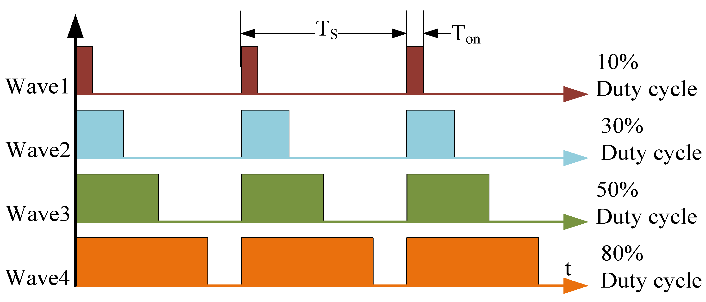
A PWM signal is a square wave with an adjustable duty cycle whose main parameters include amplitude, frequency, and duty cycle, as shown in Figure 10. A push-pull structure with the aforementioned control methods is commonly used to regulate the frequency and the duty cycle.
We used a bipolar full-bridge circuit consisting of SiC MOSFETs to generate a high-voltage PWM signal with a PC (Pockels cell) as its load, as shown in Figure 11. The advantage of using a bipolar supply is that it reduces the supply voltage by half, thereby lessening the stress on the insulation and reducing the chances of arcing over to ground. In the following section, we present a novel timing control method for continuous modulation of high-voltage pulse widths suitable for Pockels-cell-driven applications.
d u t y c y c l e = D = T o n T s

1.3.2. Applying PWM Timing Control Strategy to the PCD

In this section, we discuss two PWM timing control strategies to implement a PCD: one for generating symmetric positive and negative high-voltage pulses and one for generating unipolar positive high-voltage pulses. Both of these methods can be used to drive a PC.
(1)
Generating symmetric positive and negative PWM signals.
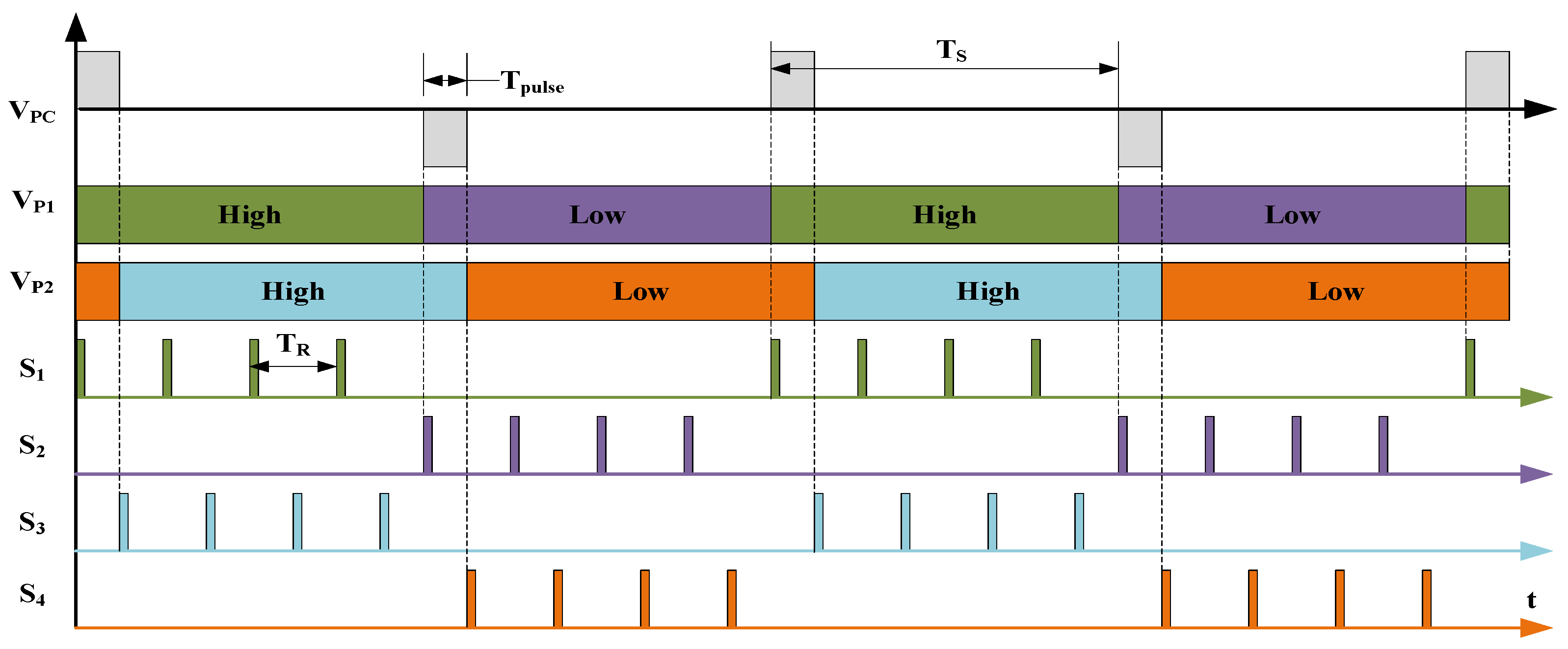
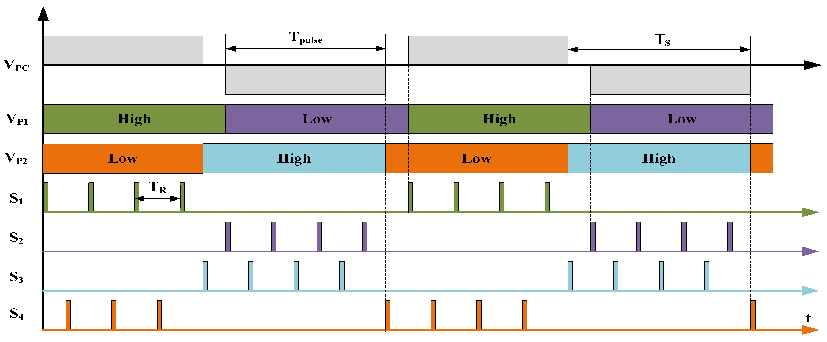
Figure 12 depicts the timing control method for each bridge arm in the case of producing a narrow duty cycle. Each MOSFET is controlled in the same way. In the case of Q 1 , S 1 generates a positive pulse through a 1:1 transformer to turn on Q 1 , resulting in a voltage of V S 2 for V P 1 . To reduce the voltage drop in V P 1 due to the leakage current, S 1 repeatedly generates a positive pulse with period T R such that Q 1 is periodically switched on to maintain the voltage V P 1 . However, in order to eliminate the effect of dead time, the interval between the last pulse of S 1 and the first pulse of S 2 must be larger than T d e a d . The control patterns of S 2 to S 4 are the same as those of S 1 . V P 1 and V P 2 behave as square waves with duty cycles of 50 percent, and the delay between them results in V P C generating symmetric positive and negative pulses with width T p u l s e and period T s .
We can tune the pulse period by changing the on-time length of each bridge arm and the pulse width by adjusting the relative positions of V P 1 and V P 2 . Figure 13 shows the waveform of V P C after increasing the duty cycle.
(2)
Generating unipolar positive PWM signals.
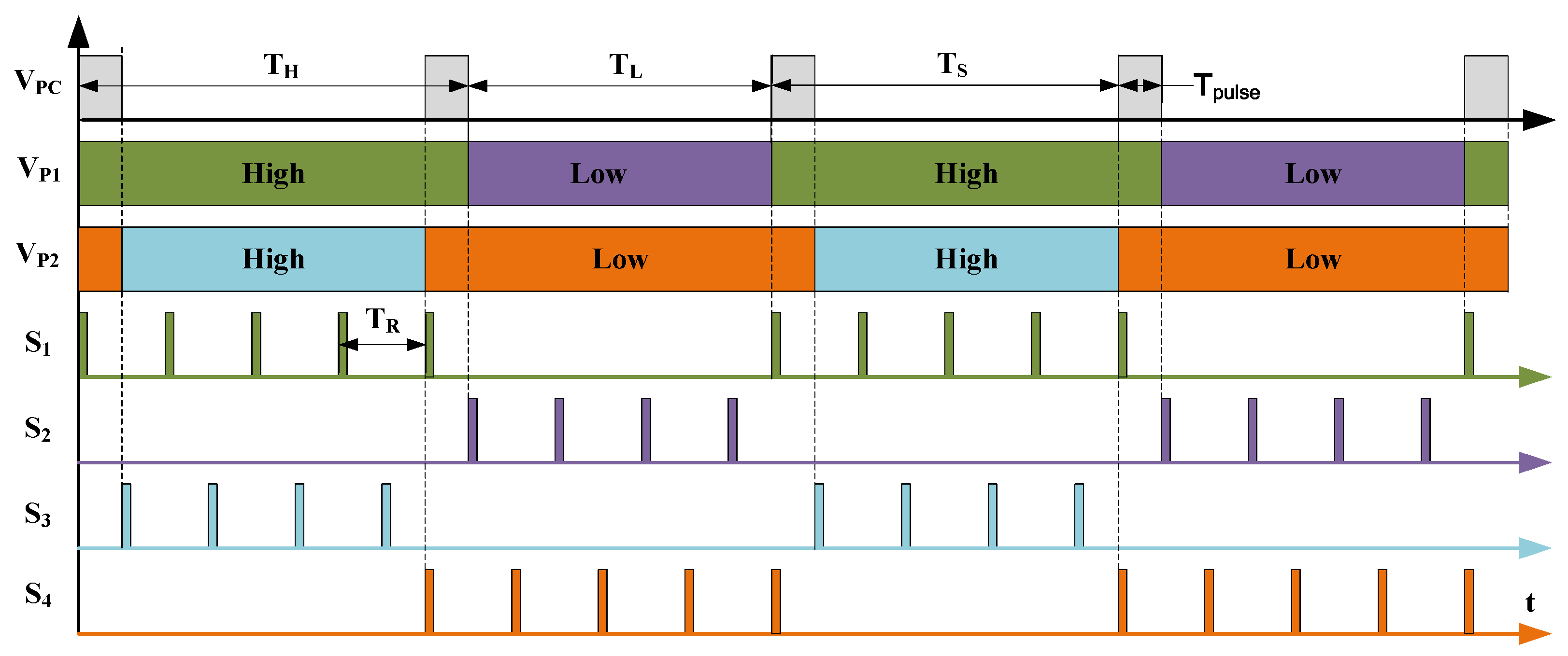
In order to generate a unipolar positive PWM signal, we can use the timing control method shown in Figure 14. The procedure is as follows: control the left bridge arm so that the length of V P 1 is T H for high levels and T L for low levels, respectively. The process is calculated using the following Equations (3) and (4):
T H = T s + T p u l s e
T L = T s T p u l s e
The high- and low-level durations of V P 2 are opposite of those of V P 1 , and they lag by period T s . In this way, V P C is a positive pulse train, and the pulse width is calculated by Equation (5).
T p u l s e = T H T L 2
According to Equation (5), we can lengthen T p u l s e by increasing T H and decreasing T L while keeping T S constant. The timing control method is illustrated in Figure 15. It should be noted that during the control of S 1 and S 2 , as well as S 3 and S 4 , a safety distance larger than the dead time should be preserved, which can be implemented easily by using counters.

1.3.3. Features of the Proposed PCD

Compared with conventional PCDs, the circuit and PWM signal-generation strategies described in this paper have the following main advantages:
(1)
High reliability: the proposed circuit uses a bipolar voltage source instead of a unipolar one, which reduces the maximum voltage by half. This can effectively lessen the stress on the insulation and reduce the chances of arcing over to ground, which could otherwise negatively affect the reliability of the system. Moreover, the circuit employs a reasonable timing control method to ensure that the on-off intervals of the upper and lower MOSFETs are longer than the dead time. The dead time is the time interval between turning off one MOSFET and turning on another MOSFET in the same arm of the bridge. If the dead time is too short or even negative, it may cause a short circuit across the DC bus and damage the devices. Therefore, by avoiding this risk, the proposed circuit enhances the reliability of the system.
(2)
Short pulse width: the proposed circuit adopts a novel timing control method that eliminates the effect of dead time on the pulse width. In conventional PCDs, the dead time limits the minimum pulse width that can be generated by the full-bridge circuit. However, in the proposed circuit, the dead time is compensated by adjusting the phase shift between the upper and lower MOSFETs in each arm of the bridge. As a result, the proposed circuit can generate extremely short pulses with a minimum pulse width of only 10 ns.
(3)
Adjustable pulse width: the proposed PWM signal generation strategy is based on the precise phase shift of the two square waves with the same frequency generated by the two pairs of bridge arms of the full-bridge circuit to control. By adjusting the phase difference between these two waves, the proposed strategy can generate PWM signals with continuously adjustable duty cycles. The duty cycle is defined as the ratio of pulse width to pulse period. Theoretically, the duty cycle can be adjusted from 0% to 100%. This means that the proposed strategy can generate pulses with various widths to meet different application requirements.
(4)
High switching speed: the proposed circuit uses transformer-coupled circuits to drive the gate terminals of the MOSFETs. This can reduce the delay time and improve the synchronization between different MOSFETs. In addition, the proposed circuit uses silicon carbide (SiC) MOSFETs as switching components instead of conventional silicon (Si) MOSFETs. SiC MOSFETs have several advantages over Si MOSFETs, such as higher breakdown voltage, lower on-state resistance, faster rising/falling times, and higher switching repetition rates. These advantages enable SiC MOSFETs to achieve higher switching speed and efficiency than Si MOSFETs.
In summary, the proposed circuit and PWM signal-generation strategies have four main advantages over conventional PCDs. First, we use a bipolar voltage source and a reasonable timing control method to reduce the chances of arcing over to ground and avoid short circuit risk, which can improve the system’s reliability. Second, a novel timing control method is employed that compensates the dead time and enables the generation of extremely short pulses with a minimum pulse width of 10 ns, which can enhance the accuracy and flexibility of laser system control. Third, we design a PWM signal-generation strategy that can adjust the duty cycle from 0% to 100%, which can provide various pulse widths for different application scenarios. Fourth, the transformer-coupled circuits and SiC MOSFETs are considered to achieve high switching speed and efficiency, which can reduce the power loss and heat dissipation of the system. Therefore, the proposed circuit and PWM signal-generation strategies are superior to conventional PCDs and can be applied to various fields that require precise control of laser systems.

2. Design and Implementation

In this section, we present our design of a PCD with the PWM signal-generation strategy mentioned above. The design specifications are shown in Table 2.

2.1. System Block Diagram and Topology

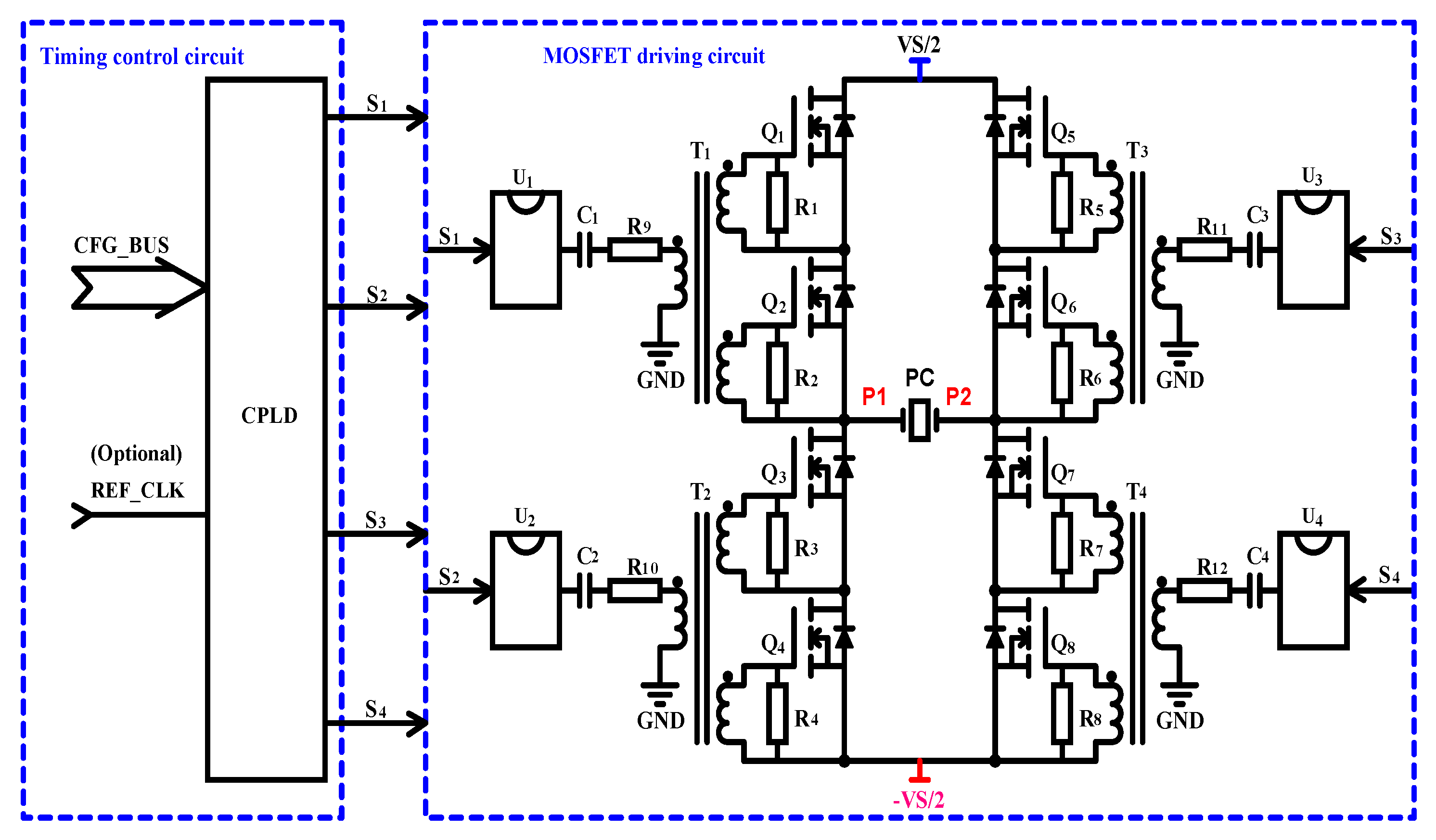
As shown in Figure 16, the PCD mentioned above is divided into two main parts. The timing control circuit on the left uses the PWM signal-generation strategy to generate the timing control signals that drive the four bridge arms. The MOSFET drive circuit on the right is used to convert the low-voltage control signal into high-voltage high pulses with adjustable frequency and pulse width.

2.1.1. MOSFET Driving Circuit

A classical transformer-coupling scheme is used to implement the MOSFET driver circuit, as it has negligible latency and can operate across higher potential differences. The primary winding of the transformer is driven by a fast MOSFET driver with low propagation delay and fast rising/falling times. Each bridge arm consists of two MOSFETs in series for increased voltage stress, driven by a 1:1:1 transformer.

2.1.2. Timing Control Circuit

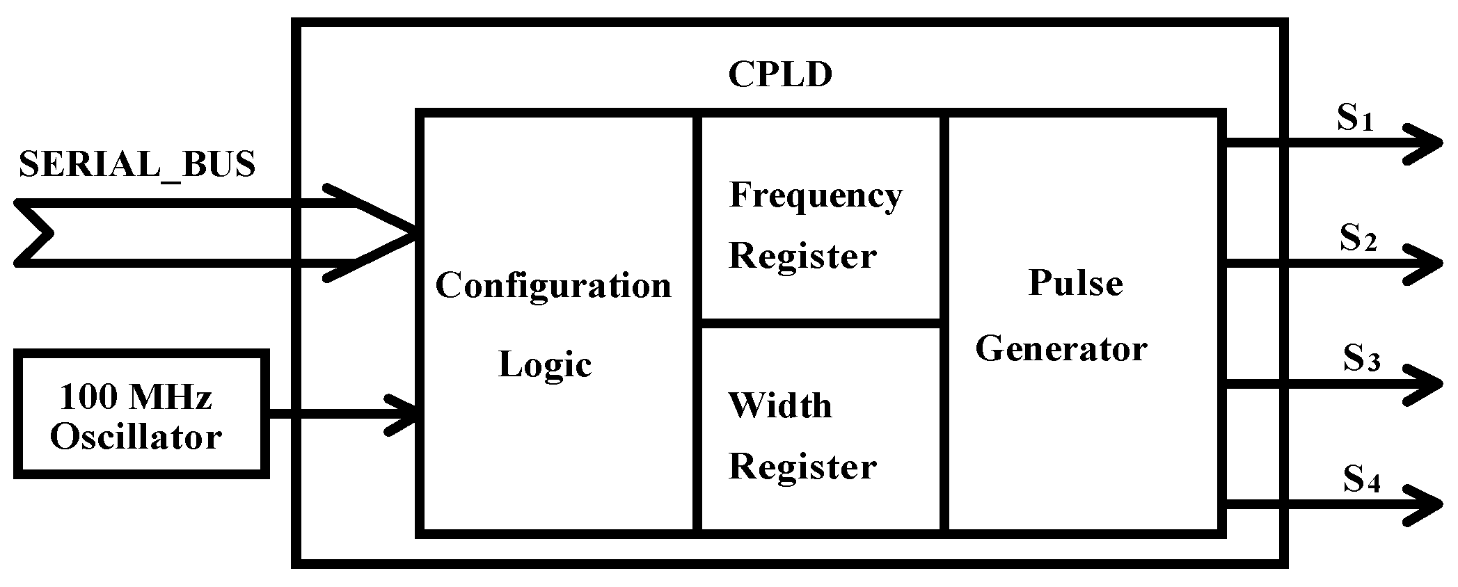
As shown in Figure 17, The timing control of the PCD is conducted using a complex programmable logic device (CPLD, Intel 5M240ZT100C5N), fed by a 100 MHz oscillator (EPSON SG-8018CB-100MHz). Parameters are set to registers via SERIAL_BUS. Configuration logic, pulse generator, frequency and width registers are modules inside the CPLD. The configuration logic loads the input data into the frequency and width registers after serial-to-parallel conversion. The register has a bit depth of 24 bits and can be reconfigured as needed during design. The pulse generator then generates timing control signals S 1 S 4 based on these two parameters, the working principle of which is described in detail in the next paragraph.

2.2. PWM Timing Control Method

The principle of the PWM signal-generation strategy was described in the previous section. As an example, in this section, we describe the implementation of the timing control method for generating symmetric positive and negative pulses.
In order for V P C to generate a pulse with period T S and width T p u l s e , all that is required is for V P 1 and V P 2 to generate a square wave with period 2 T s and duty cycle 50%, and for V P 2 to delay T p u l s e relative to V P 1 , as shown in Figure 12.
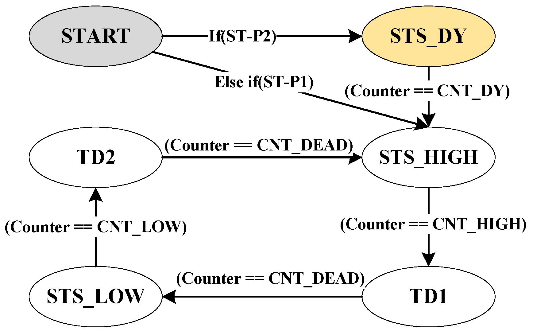
We adopt an approach where the timing of S 1 S 2 and S 3 S 4 is controlled by two state machines, ST-P1 and ST-P2, respectively, as shown in Figure 18. There are five states—STS_DY, STS_HIGH, TD1, TD2, and STS_LOW— each of which is controlled by a counter. When the current state counter is completed, it jumps to the next state. Given the period T s , the pulse width T p u l s e , and the dead time T d e a d , the counting values of the five states can be calculated as follows.
  • Duration of STS_DY: CNT_DY = T p u l s e ;
  • Duration of STS_HIGH: CNT_HIGH = T s T d e a d ;
  • Duration of STS_LOW: CNT_LOW = T s T d e a d ;
  • Dead time is T d e a d : CNT_DEAD = T d e a d = 50 ns;
  • High-level duration of V P 1 and V P 2 : T V P H = T s ;
  • Low-level duration of V P 1 and V P 2 : T V P L = T s .
First, in the ST-P1 state machine, STS_HIGH and STS_LOW control S 1 and S 2 , respectively, to generate pulses with period T R . Second, in the ST-P2 state machine, STS_DY and STS_HIGH control S 3 to generate pulses with period T R , and STS_LOW controls S 4 to generate pulses with period T R . Finally, all control-signal-generated pulses are forbidden in the TD1 and TD2 regimes. The effect of dead time is avoided by the timing control method described above for S 1 S 4 , and the resulting waveforms for V P C with adjustable frequency and pulse width are shown in Figure 19.

2.3. Selection of Switches and Discrete Components

As mentioned above, switching devices are the main factors affecting the PCD performance, and SiC MOSFETs are preferred because of their high-voltage stress, fast rising/falling times, and low cost, and they can be used to design PCDs with simple circuit structures. As shown in Figure 16, four CREE SiC MOSFETs C3M0350120D were used in this design, and the main parameters are shown in Table 3. The resistors R 1 R 8 (100 Ω ) provide low impedance channels to release the gate charge.
Gate drive transformers are widely used to drive high-voltage circuits. High-voltage gate drive ICs are smaller and more convenient, but they have significant turn-on and turn-off delays and lower insulation voltages than transformers. Therefore, we used gate drive transformers made with manganese-zinc ferrite magnetic rings. The turn ratio is 1:1:1, and the inductance is approximately 10 μH.

2.4. Transformer-Coupled Gate Drive Circuits

In order to increase the switching speed of the SiC MOSFETs, the transformers are driven by ultrafast low-voltage MOSFET drivers (IXDN614 U 1 U 4 ), which can source and sink 14 A of the peak current. The coupling capacitors C 1 C 4 must be placed in series with the primary winding of the transformers to provide the reset voltage for the magnetizing inductance.
The capacitances of C 1 C 4 are calculated by the following Equation (6) [30].
C C = Q G Δ V C + V D R V × 1 D × D Δ V C × R G S × f D R V
C C : Coupling capacitance;
Q G : Total gate charge, 19 nC;
V D R V : Output voltage of IXDN614, 18 V;
f D R V : Switching frequency, < 10 6 Hz;
D: Duty cycle at f = 10 6 Hz, 0.2 ;
Δ V C :Voltage ripple across C C , V D R V × 1 % ;
R G S : Gate to source resistor, 100 Ω .
C C = 19 × 10 9 0.01 × 18 + 18 × 1 0.2 × 0.2 0.01 × 18 × 100 × 10 6 105.6 × 10 9 + 160 × 10 9 265.6 nF
Therefore, C 1 C 4 were determined to be 470 nF by taking into account the sufficient margin.
As the primary winding of the isolation transformer can be equivalently viewed as an inductor L and can form an L-C resonator with the coupling capacitor, the resistors R 9 R 12 should be inserted in series with C 1 C 4 , respectively, to damp this L-C resonance. The values of R 9 R 12 are shown in Equation (7).
R C 2 × L M C C 10 Ω

3. Experiment Results

3.1. Experiment Setups

We use the experimental setup shown in Figure 20 to test the performance of the PCD, which directly drives a PC (BBO Pockels cell, 6.7 pf, 2.03 kV). Five additional instruments are included in the block diagram, including a power supply PCD-HV-250 (250 W, 1.0–3.0 kV) to provide high voltage, a cooling system (MPS-1500A-22) to cool the MOSFETs, an oscilloscope HDO4035 (350 MHz, 2.5 GS/s), and two single-ended probes PPE6KV-A (500 MHz, 2.8 pF, 1 kV RMS) to record the pulse waveforms. A Q-switched slab laser is also used to demonstrate the function of the PCD.

3.2. Small Duty Cycle Test

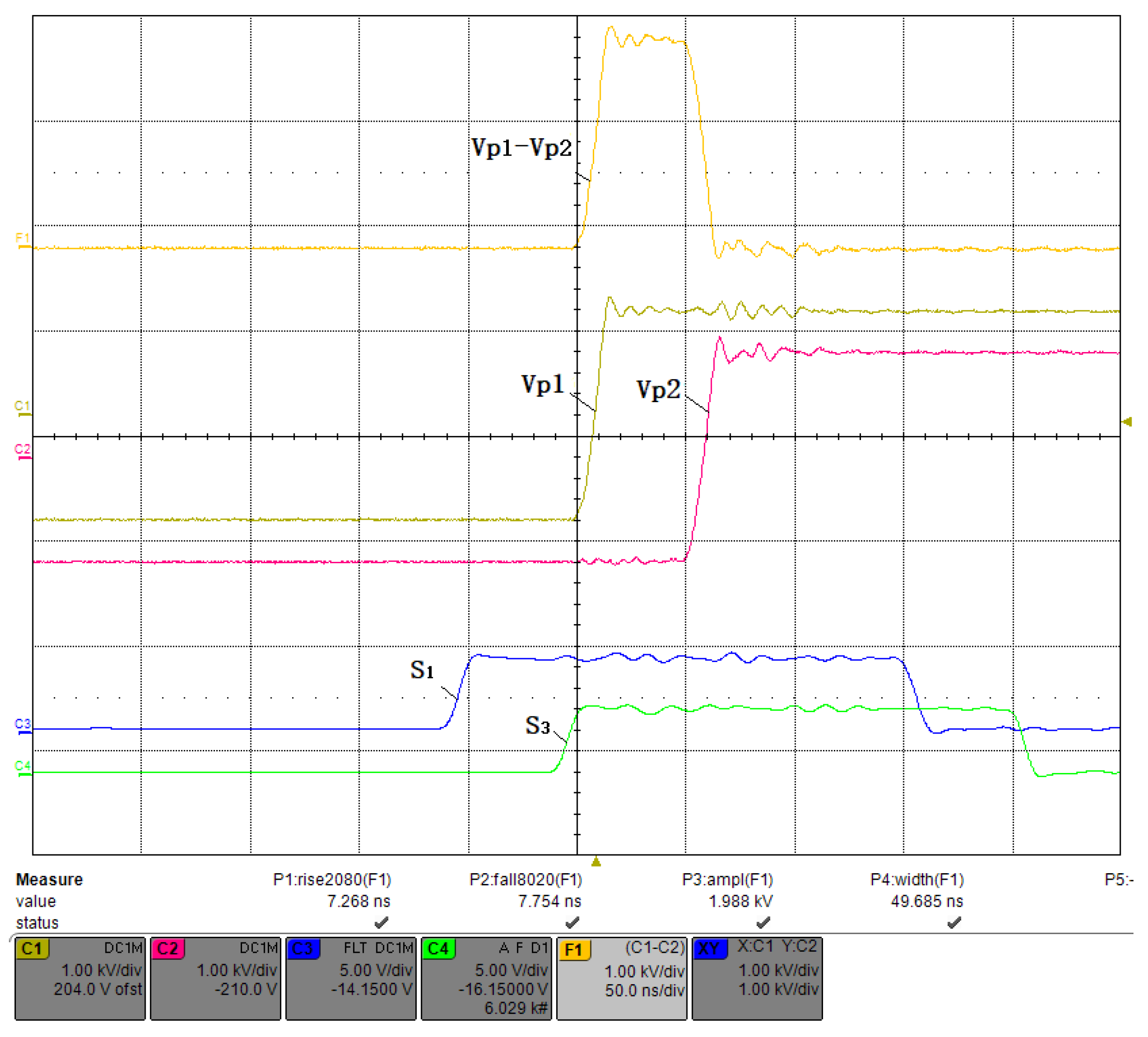
Figure 21 shows a positive short pulse with a width of 50 ns and a duty cycle of 0.005%. The rising and falling times were approximately 7.3 ns and 7.8 ns, respectively, with a repetition rate of 1 kHz and an amplitude of approximately 2.0 kV. Channels C 1 and C 2 show the waveforms of V P 1 and V P 2 , channels C 3 and C 4 show the waveforms of S 1 and S 3 , and channel F 1 shows the waveform of V P 1 V P 2 . Since V P 1 and V P 2 are controlled by S 1 and S 3 , respectively, the width of F 1 is determined by the delay between S 1 and S 3 . It also can be adjusted by shifting their relative positions. The delay between S 1 to V P 1 and S 3 to V P 2 is caused by the MOSFET driver circuit.
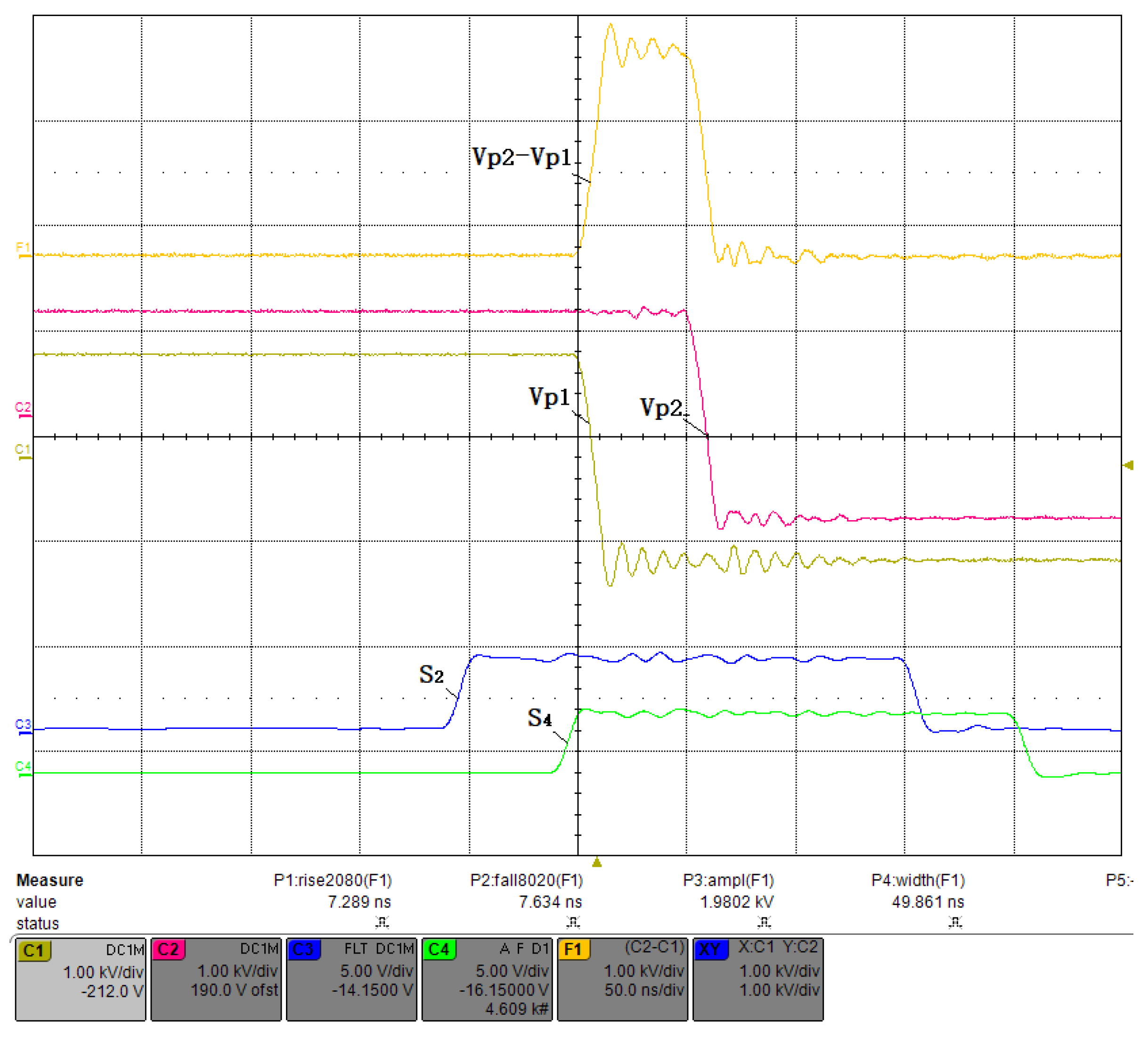
As shown in Figure 22, channels C 3 and C 4 are changed to S 2 and S 4 , respectively. After one cycle, S 2 and S 4 generate pulses successively, and V P 1 and V P 2 then switch from positive to negative voltages and generate pulses with widths which is equal to the phase delay of V P 1 and V P 2 represented by V P 2 V P 1 .
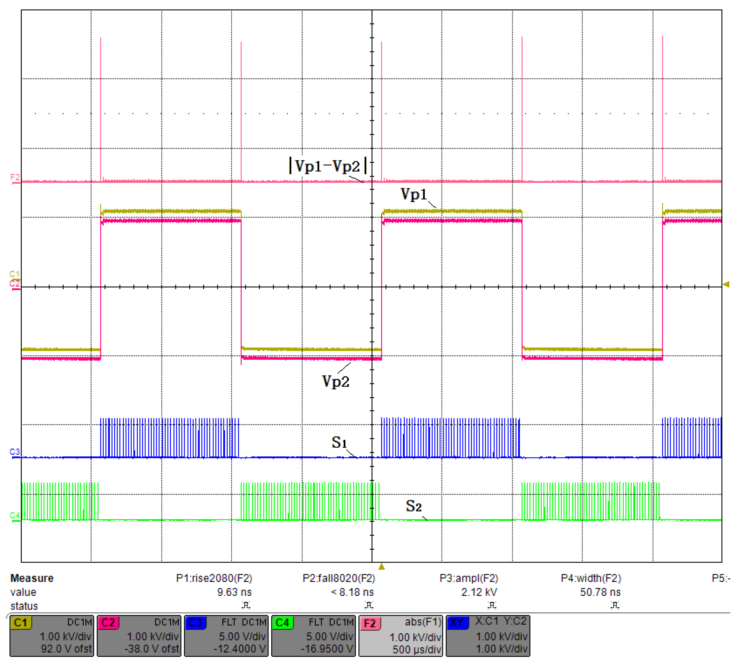
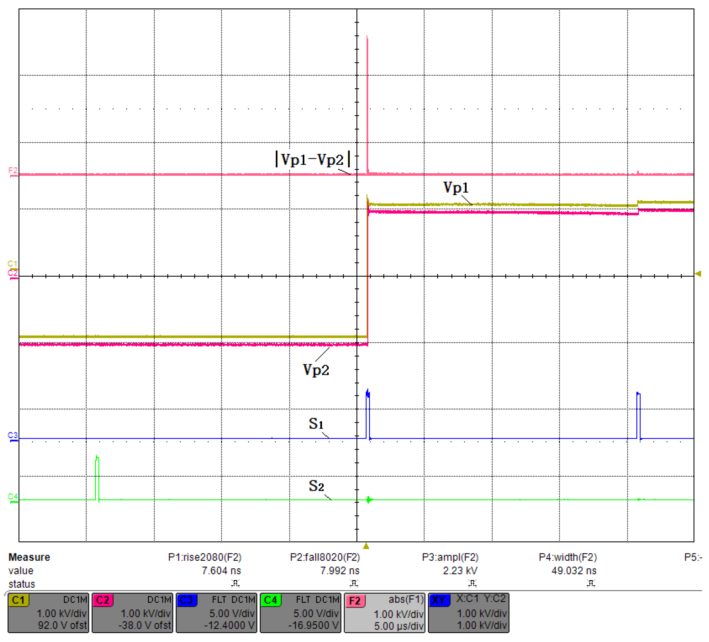
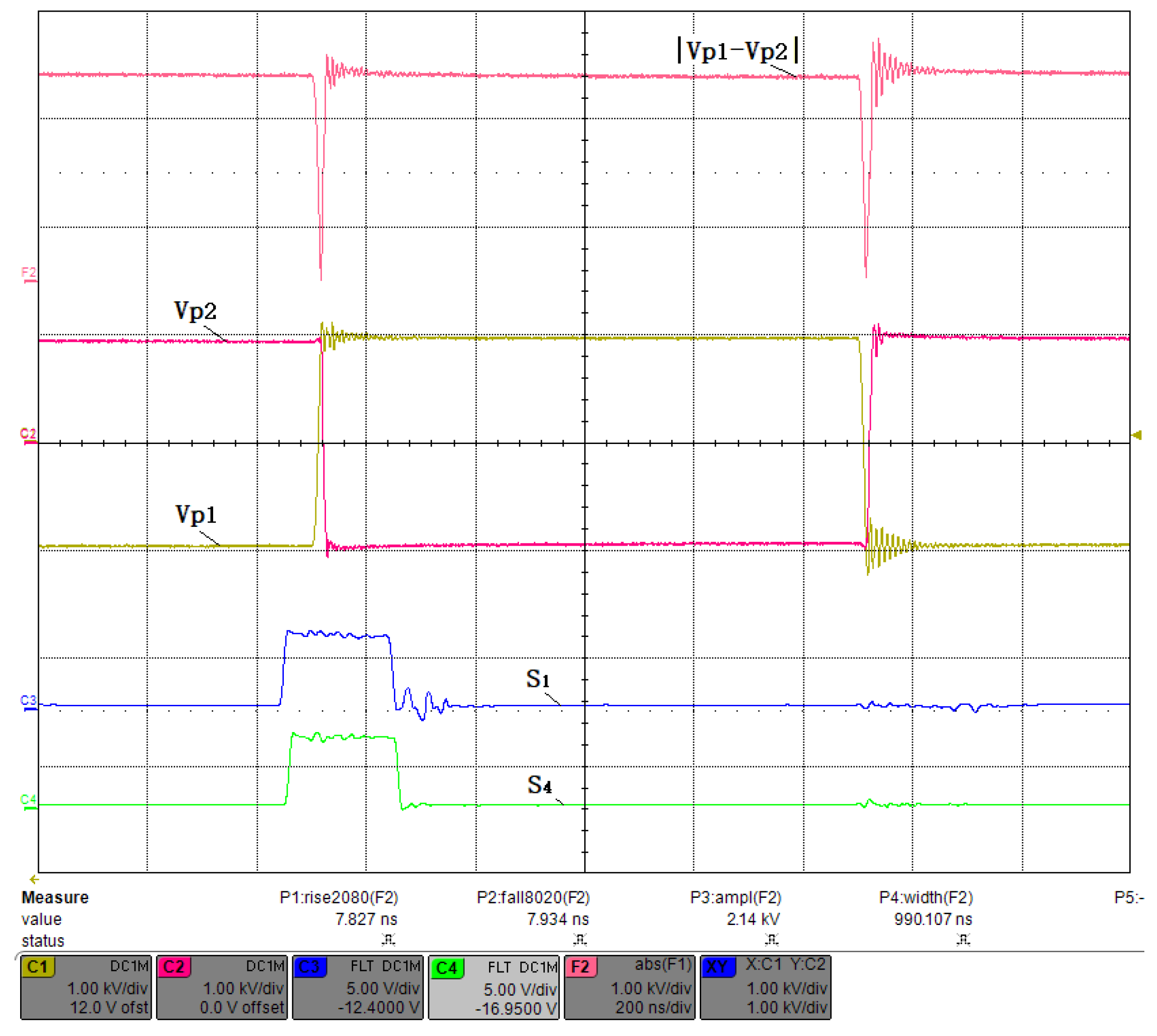
The recharging method is shown in Figure 23, where the display window is adjusted to 500 us/div, channels C 3 and C 4 are changed to S 1 and S 2 , respectively, and channel F 2 displays the waveform | V P 1 V P 2 |. S 1 and S 2 are periodic pulses with a frequency of 50 kHz and a width of 200 ns, which proved to be a suitable set of parameters to control the high and low levels of V P 1 . We can also see ripples on V P 1 and V P 2 caused by repeated charging. V P 2 is controlled by S 3 and S 4 in the same way and is not shown in the figure.
Figure 24 is a zoomed-in version of Figure 23. Although S 1 and S 2 are signals that control the opening of the upper and lower arms of the full bridge circuit, respectively, the time interval between them can not damage the SiC MOSFETs as long as it is larger than the dead time. We do this by adding a protected region equal to the dead time at the end of each period. In this protected region, the pulses generated by S 1 and S 2 are canceled.
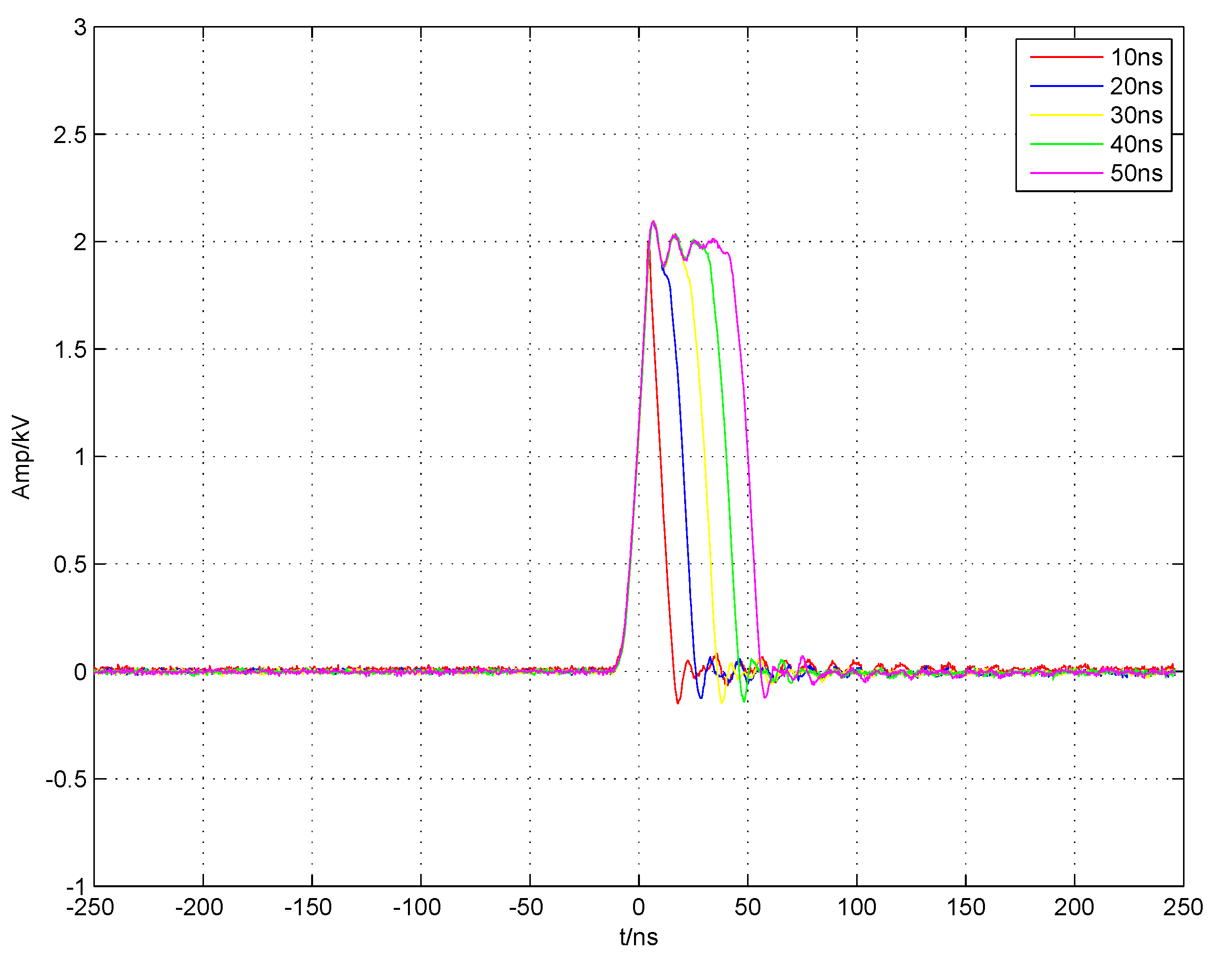
Finally, to precisely demonstrate the pulse width adjustment function, we capture five data sets using an oscilloscope and plot them on a single figure for comparison. Figure 25 shows high-level pulses with widths extending from 10 ns to 50 ns in 10 ns steps.

3.3. Fifty Percent Duty Cycle Test

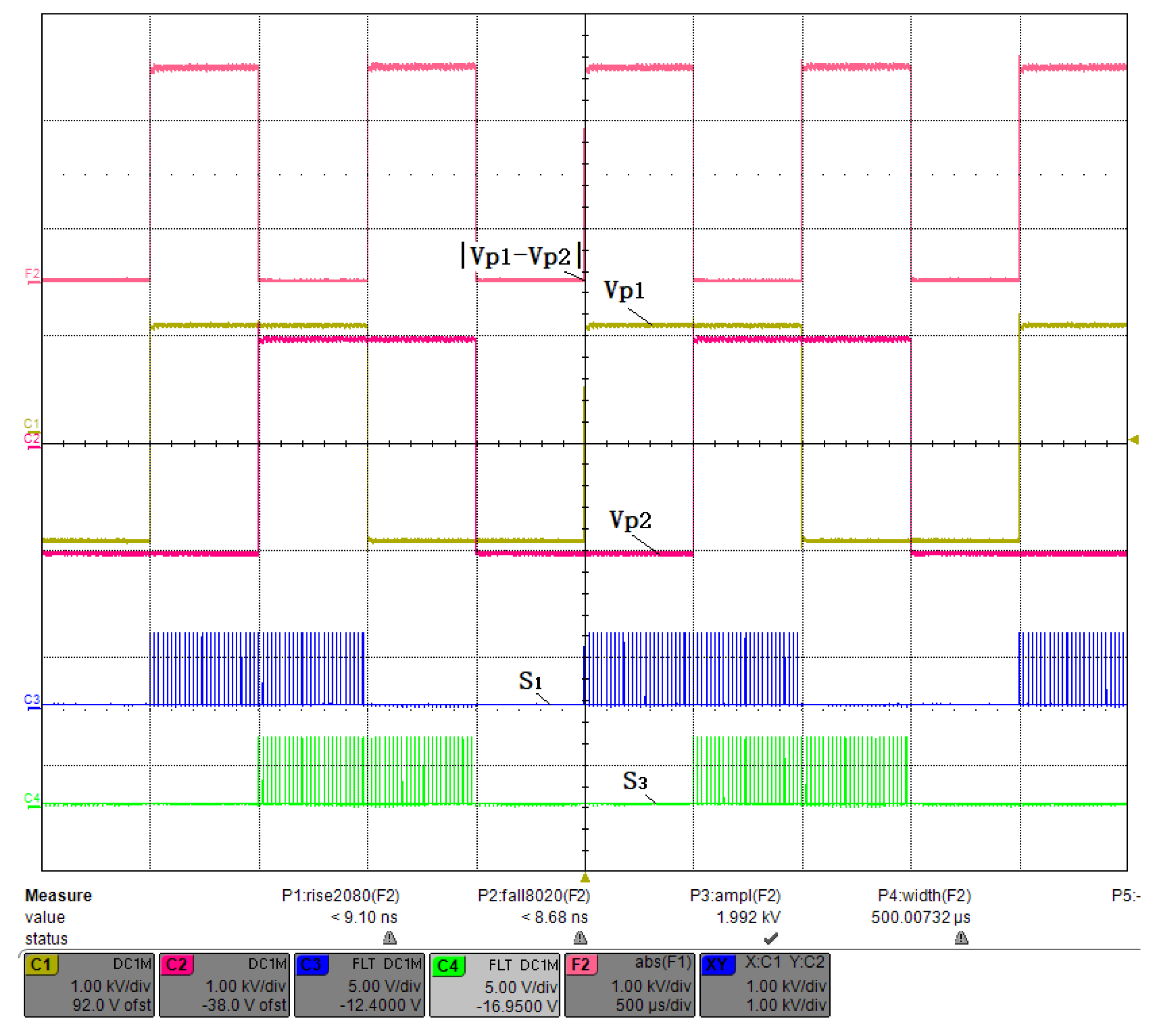
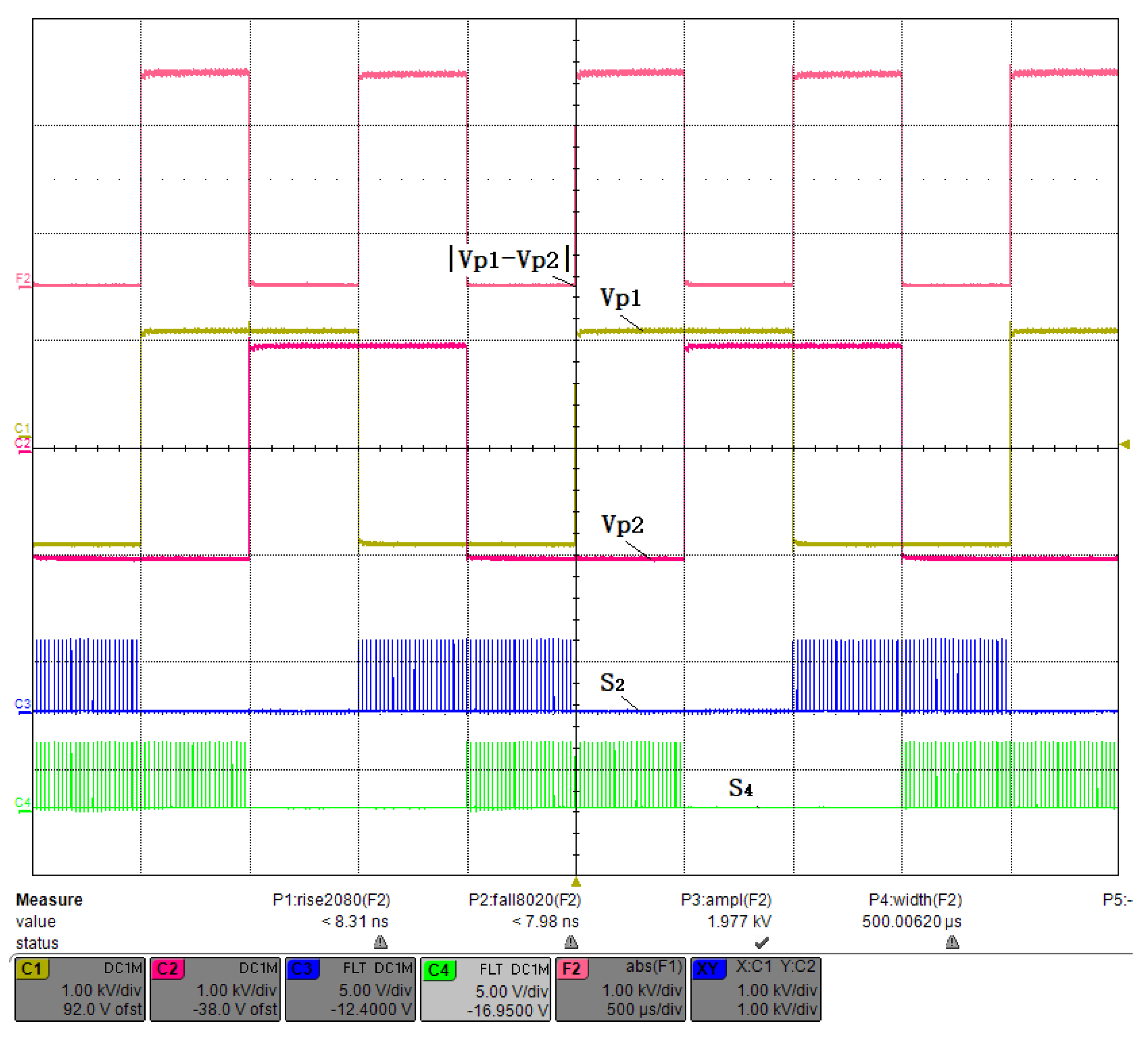
In Figure 26, channels C 3 and C 4 are changed to S 1 and S 3 , respectively, which control V P 1 and V P 2 to switch from low level to high level and produce a phase shift of 90 degrees. The channel F 2 displays the waveform of | V P 1 V P 2 |, which shows a square waveform with a width of 500 us and a duty cycle of 50% at a frequency of 1 kHz and an amplitude of approximately 2.0 kV. S 2 and S 4 control V P 1 and V P 2 to switch from high level to low level, respectively, which are shown in Figure 27.

3.4. Large Duty Cycle Test

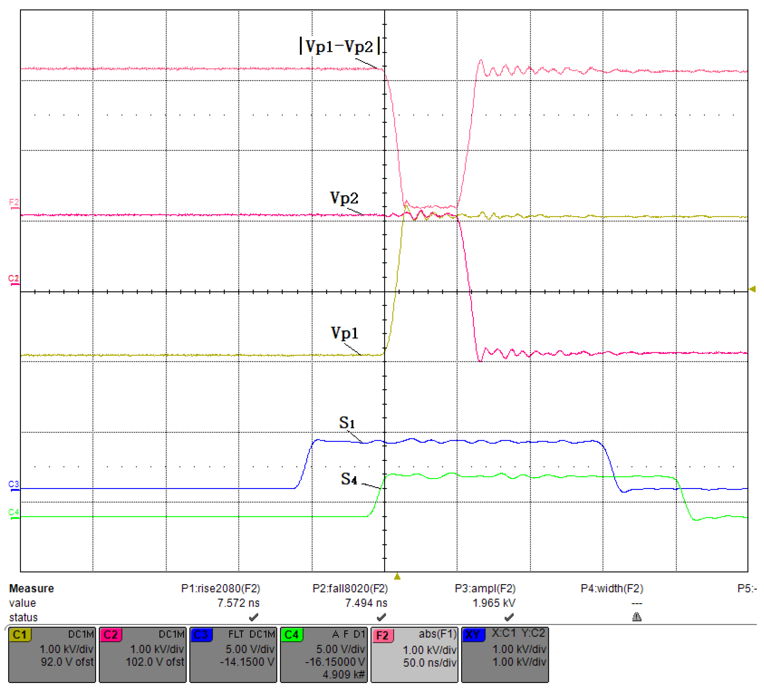
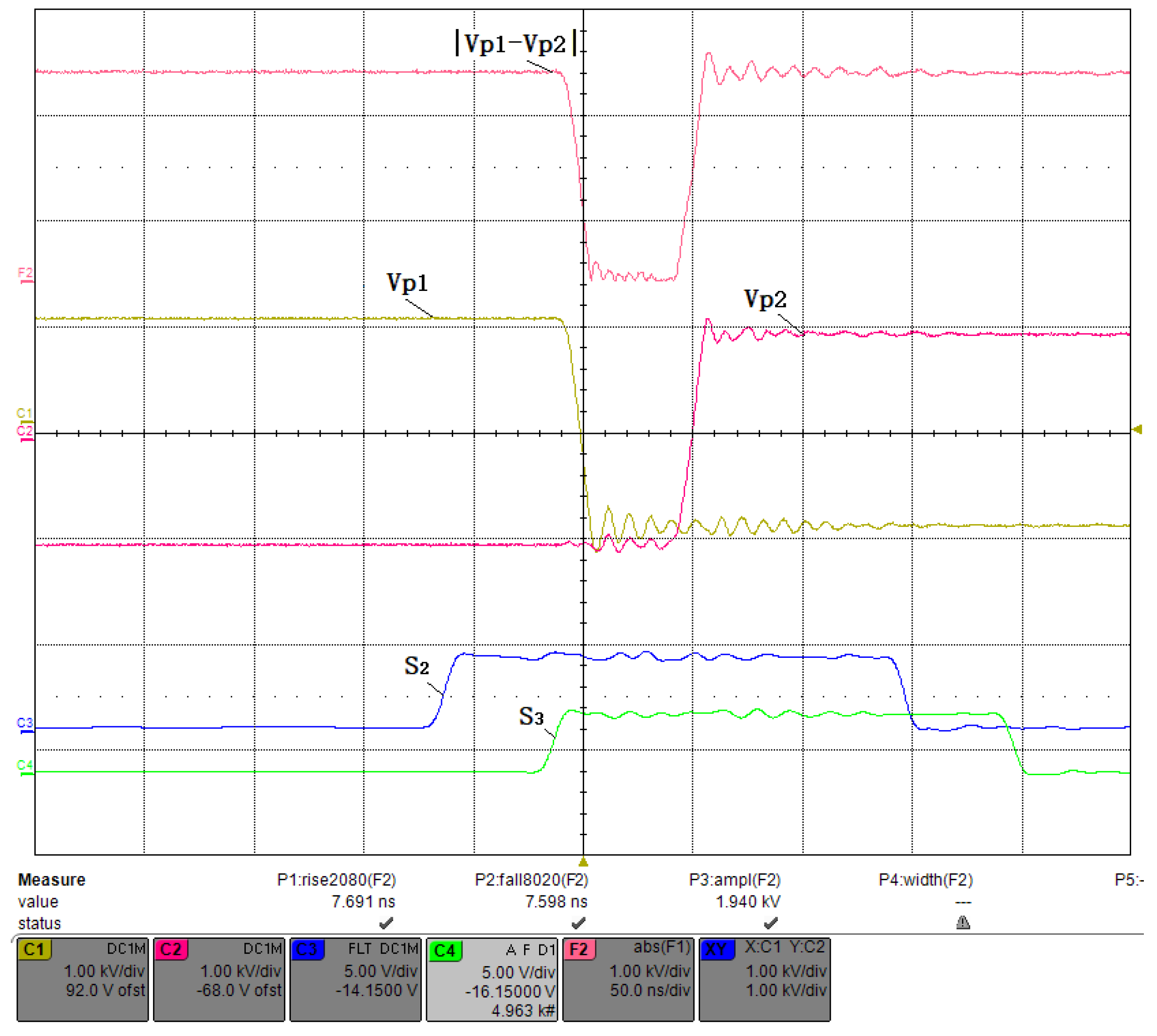
Figure 28 shows the waveform of a negative pulse with a width of 50 ns and a large duty cycle of 99.995%. The rising and falling edges are approximately 7.6 ns and 7.5 ns, respectively, with 1 kHz frequency and approximate 2.0 kV amplitude. S 1 controls V P 1 to switch from low level to high level and S 4 controls V P 2 to switch in the opposite direction, and the delay between the two causes | V P 1 V P 2 | to generate a low pulse. The pulse width can be changed by adjusting the delay time between S 1 and S 4 . In addition, Figure 29 shows that S 2 and S 3 can be used in a similar way to generate a low pulse in the next cycle.
We captured five data sets via an oscilloscope in the same way and plotted them on a figure for comparison. Figure 30 shows low pulses with widths extending from 10 ns to 50 ns in 10 ns steps.

3.5. High-Repetition-Rate Test

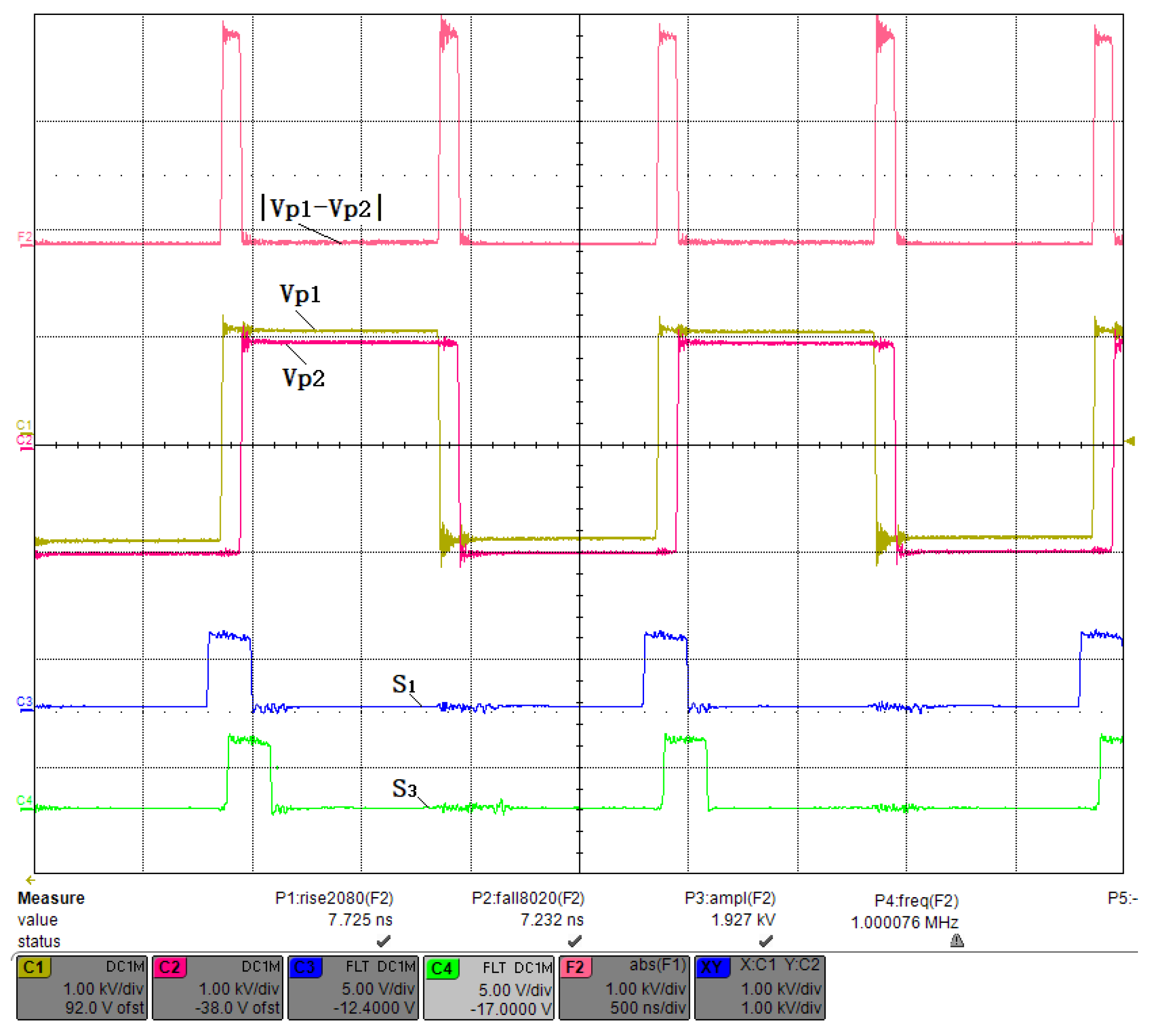
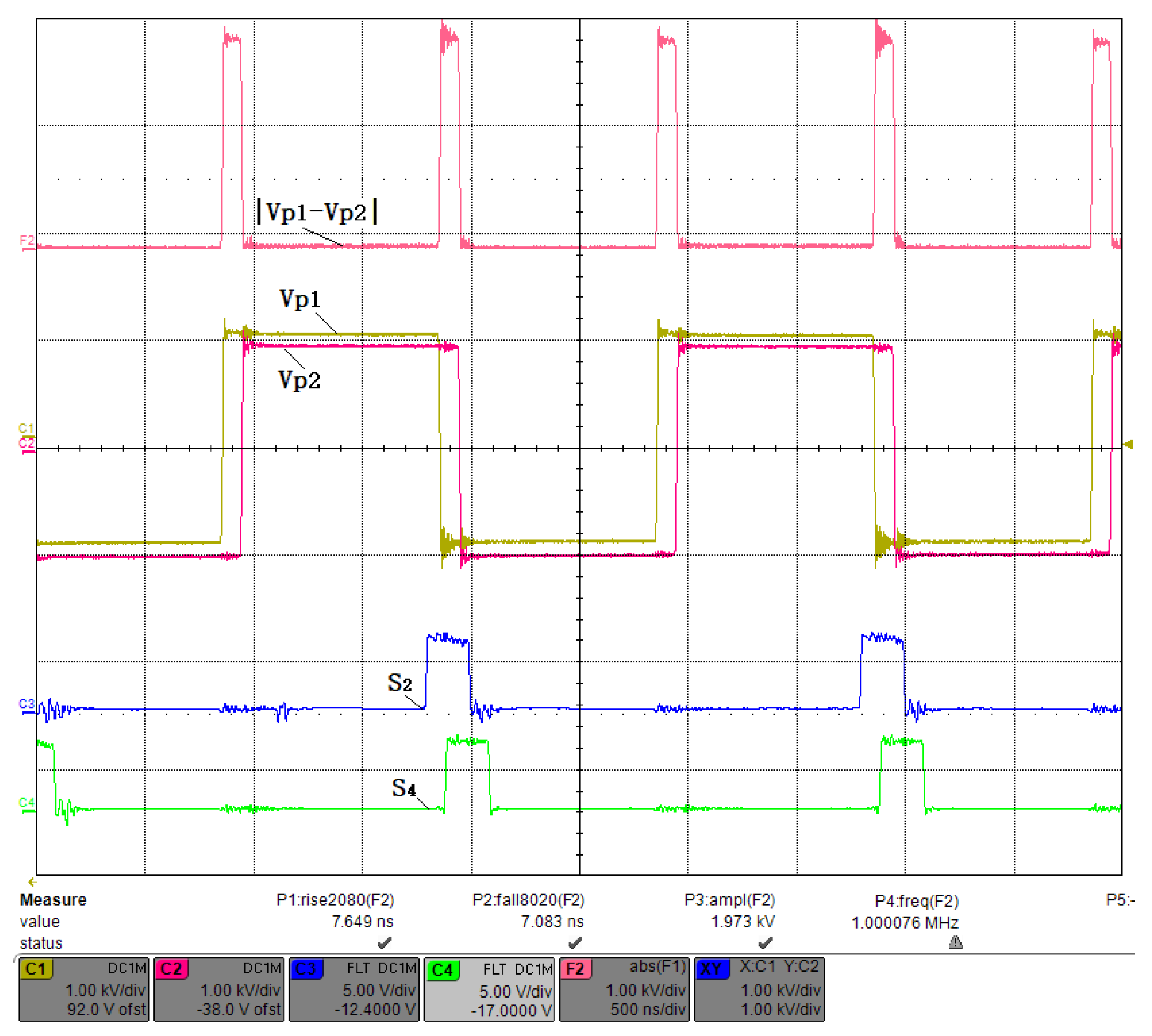
Figure 31 shows the waveform with a repetition rate of 1 MHz and an operating voltage of approximately 2.0 kV. Due to the high switching loss of MOSFETs, a cooling system is required for heat dissipation. S 1 and S 3 control the switching of V P 1 and V P 2 from low to high levels, and the delay between the two causes | V P 1 V P 2 | to generate high pulses. As shown in Figure 32, S 2 and S 4 control V P 1 and V P 2 to switch in opposite directions and cause | V P 1 V P 2 | to generate pulses in the next cycle. When the PCD is operated at a high repetition rate, the duty cycle is controlled in the same way as for the 1 kHz repetition rate. Figure 33 and Figure 34 show waveforms with duty cycles of 1% and 99%, respectively. Moreover, when the repetition rate is larger than 50 kHz, S 1 S 4 does not need to generate periodic repeated charging pulses. The 0% and 100% duty cycles can be obtained by generating uninterrupted 50 kHz pulses from S 1 , S 3 and S 1 , S 4 , respectively. Thus, this is true for all output frequencies of the PCD.

3.6. Power Loss Test

The PCD power loss is dominated by the power consumed in the PC P P C , the switching loss of SiC MOSFETs P S W and the power loss of the control circuits P C T R L . The PC can be regarded as an equivalent capacitor C P C , so P P C is given by the following equation (8).
P P C = 1 2 × C P C × V S 2 × f s w
Where VS is the quarter-wave voltage and f s w is the switching frequency. The PC used in this work has an equivalent capacitance of about 6.7 pF and a quarter-wave voltage VS of about 2030 V. As an example, at f s w of 1 MHz, P P C = 13.4 W. The remaining two power losses are difficult to estimate accurately.
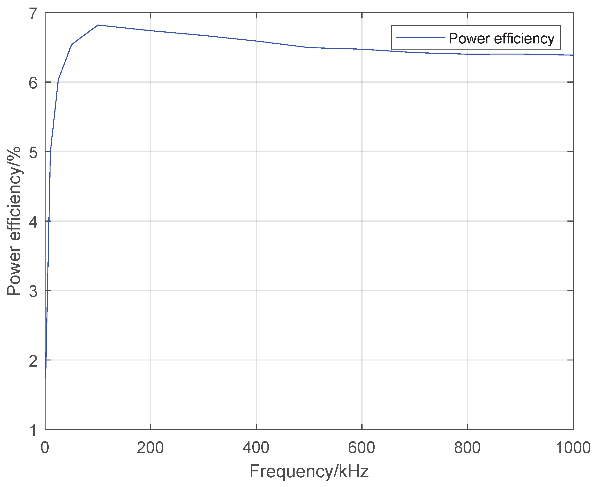
In fact, we can obtain the power consumption of these three parts by measuring the power consumption of the low-voltage supply and the power consumption of the high-voltage supply with and without PC load. The results of the test are shown in Figure 35. For a high-voltage pulse of 2.0 kV, the power consumption of the three parts varies almost linearly with frequency. The maximum power consumption of P S W , P P C , and P C T R L is about 202.4 W, 14.2 W, and 5.7 W, respectively, when operating at 1 MHz. P C T R L has a static power consumption of about 0.6 W. As a result, the calculated power efficiency is rather small, about 6.4% at an operating voltage of 2.0 kV and a repetition frequency of 1 MHz, which are also shown in Figure 36.

3.7. PCD Test in a Slab Laser

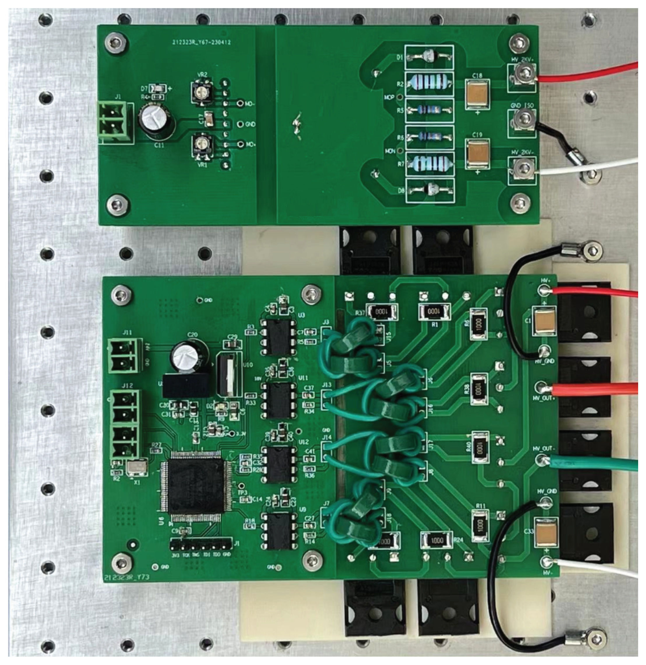
Figure 37 shows a photograph of the developed PCD, including a high-voltage bipolar power supply. We verify the function of this PCD in a home-built slab laser operating in the “Off-type” mode. The quarter-wave voltage of the PC is approximately 2.03 kV.
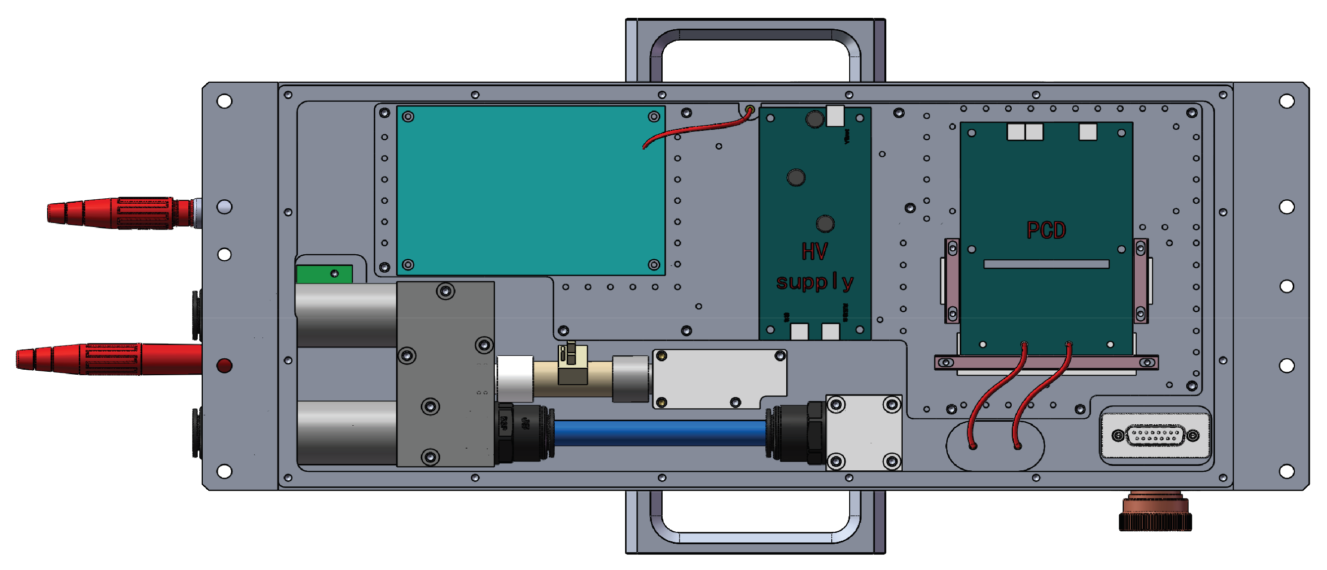
In Figure 38, the PCD and HV supply modules are measured approximately 4.5” × 3.0” and 4.5” × 2.0”, respectively, for easy installation in the electronic compartment. The Q-switched high-voltage signal is wired through the substrate to the PC mounted in the optical compartment. The HV supply module (PCD-HV-08) is a low-power version of about 8 W. Since the slab laser uses water cooling, the MOSFETs are mounted against the substrate, indicating that the PCD can share a large chiller in the laser system.
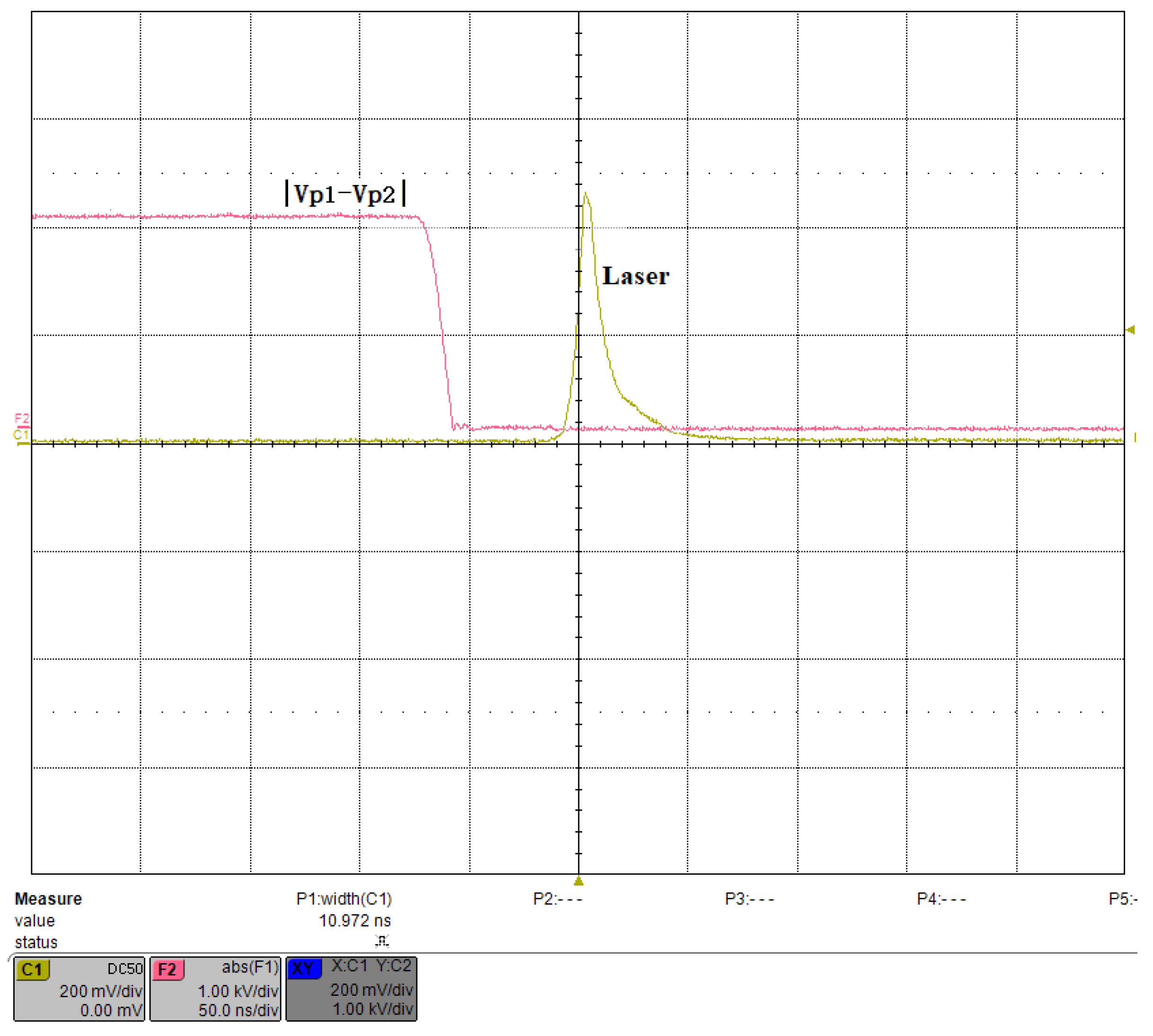
The PCD generates waveforms with a duty cycle of 99%, a low-level width of 1 μs, and a repetition rate of 10 kHz. A 1064 nm laser pulse with a width of approximately 11.0 ns and a power of 100 W was obtained, and the waveform is shown in Figure 39.

4. Conclusions

In this paper, we presented a novel PWM signal-generation strategy applied to a transformer-coupled, bipolar-power-supplied SiC MOSFET-switched full-bridge circuit. By using this strategy to control the timing of the primary winding of the transformer, the effect of dead time is removed, and the limitation of the volt-second product of the transformer on the width of the drive signal is resolved. Compared with existing products, this PCD has the advantage of producing continuously tunable pulses with a step of 10 ns, and there is no restriction on the maximum width, which allows it to be widely used in Q-switched lasers, pulse pickers, and regenerative amplifiers. The experimental results show that the circuit has a rising time of approximately 7.3 ns and a falling time of approximately 7.8 ns, with a maximum voltage of approximately 2.0 kV, and a maximum repetition rate of 1 MHz.

Author Contributions

In this work, Y.W. conceived and designed, performed, and analyzed the experiments and wrote the paper under the guidance of W.L. and T.Z., J.C. and X.S. provided some suggestions on the background, introduction, and conclusion. All authors have read and agreed to the published version of the manuscript.

Funding

This work was supported in part by the Civil Space Technology pre-research project under Grant D020305; in part by the all-solid-state ultraviolet and mid-infrared laser source technology project under Grant 2022YFC3700401.

Institutional Review Board Statement

Not applicable.

Informed Consent Statement

Not applicable.

Data Availability Statement

Not applicable.

Conflicts of Interest

The authors declare no conflict of interest.

References

  1. Shimony, Y.; Burshtein, Z. Repetitive Q-switching of a CW Nd:YAG laser using Cr/sup 4+/:YAG saturable absorbers. IEEE J. Quantum Electron. 1996, 32, 305–310. [Google Scholar] [CrossRef]
  2. Linne, M.; Baer, T. Q-Switching of Diode Pumped Solid State Lasers. In Proceedings of the 1988 Los Angeles Symposium–O-E/LASE ’88, Los Angeles, CA, USA, 11–17 January 1988; pp. 110–114. [Google Scholar]
  3. Hnninger, C.; Paschotta, R.; Morier-Genoud, F.; Moser, M.; Keller, U. Q-switching stability limits of continuous-wave passive mode locking. J. Opt. Soc. Am. 1999, 16, 46–53. [Google Scholar] [CrossRef]
  4. Balzer, J.C.; Schlauch, T.; Hoffmann, T.; Klehr, A.; Erbert, G.; Hofmann, M.R. Modelocked semiconductor laser system with pulse picking for variable repetition rate. Electron. Lett. 2011, 47, 1387–1388. [Google Scholar] [CrossRef]
  5. Zhao, Z.; Mernick, K.; Costanzo, M.; Minty, M. An ultrafast laser pulse picker technique for high-average-current high-brightness photoinjectors. Nucl. Instrum. Methods Phys. Res. Sect. Accel. Spectrometers Detect. Assoc. Equip. 2020, 959, 163586.1–163586.5. [Google Scholar] [CrossRef]
  6. Xie, X.; Simon, J.D. High energy and tunable picosecond laser pulses at 1 kHz: Synchronously pumping a dye laser with a mode-locked, Q-switched and cavity dumped Nd:YAG laser system. Opt. Commun. 1989, 69, 303–307. [Google Scholar] [CrossRef]
  7. Kornev, A.F.; Pokrovskiy, V.P.; Gagarskiy, S.V.; Yu, F.Y.; Gnatyuk, P.A.; Kovyarov, A.S. 946nm Nd:YAG laser with cavity dumping. Opt. Lett. 2018, 43, 3457–3460. [Google Scholar] [CrossRef] [PubMed]
  8. Okishev, A.; Battaglia, D.; Begishev, I.; Zuegel, J. Highly stable, diode-pumped, cavity-dumped Nd:YLF regenerative amplifier for the OMEGA laser fusion facility. In Advanced Solid State Lasers; Optica Publishing Group: Washington, DC, USA, 2002; Volume 68, p. WB12. [Google Scholar] [CrossRef] [Green Version]
  9. Okishev, A.V.; Zuegel, J.D. Highly stable, all-solid-state Nd:YLF regenerative amplifier. Appl. Opt. 2004, 43, 6180–6186. [Google Scholar] [CrossRef]
  10. Murray, J.E.; Lowdermilk, W.H. ND:YAG regenerative amplifier. J. Appl. Phys. 1980, 51, 3548–3556. [Google Scholar] [CrossRef]
  11. Calendron, A.L.; Çankaya, H.; Kärtner, F.X. High-energy kHz Yb:KYW dual-crystal regenerative amplifier. Opt. Express 2014, 22, 24752–24762. [Google Scholar] [CrossRef] [PubMed]
  12. Melnikov, K. Electro-optic Q-switch driver design specifics. Proc. Soc. Photo-Opt. Instrum. Eng. 2011, 7822, 39–45. [Google Scholar]
  13. Plourde, B.; Mack, M.E.; Verro, E. Simple, fast rise time, high repetition rate Pockels cell driver. Rev. Sci. Instrum. 1980, 51, 549–550. [Google Scholar] [CrossRef]
  14. Mccaulay, J.; Byrne, H.; Dennis, W.M.; Shen, G.; Blau, W. Thyratron-based Pockels cell driver for single pulse switch-out in mode-locked lasers. Opt. Laser Technol. 1989, 21, 401–405. [Google Scholar] [CrossRef]
  15. Dharmadhikari, A.K.; Dharmadhikari, J.A.; Adhi, K.P.; Mehendale, N.Y.; Aiyer, R.C. Low cost fast switch using a stack of bipolar transistors as a pockel cell driver. Rev. Sci. Instrum. 1996, 67, 4399–4400. [Google Scholar] [CrossRef]
  16. Dharmadhikari, J.A.; Dharmadhikari, A.K.; Mehendale, N.Y.; Aiyer, R.C. Low cost Pockels cell driver for pulsed solid state lasers. Opt. Laser Technol. 1998, 30, 447–450. [Google Scholar] [CrossRef]
  17. Fulkerson, E.S.; Norman, D.C.; Booth, R. Driving pockels cells using avalanche transistor pulsers. In Proceedings of the Digest of Technical Papers. 11th IEEE International Pulsed Power Conference (Cat. No. 97CH36127), Baltimore, MD, USA, 29 June–2 July 1997; IEEE: Piscataway Township, NJ, USA, 1997; Volume 2, pp. 1341–1346. [Google Scholar]
  18. Bishop, A.I.; Barker, P.F. Subnanosecond Pockels cell switching using avalanche transistors. Rev. Sci. Instrum. 2006, 77, 3066. [Google Scholar] [CrossRef]
  19. Li, J.; Zhao, Z.; Sun, Y.; Liu, Y.; Ren, Z.; He, J.; Cao, H.; Zheng, M. A hybrid pulse combining topology utilizing the combination of modularized avalanche transistor Marx circuits, direct pulse adding, and transmission line transformer. Rev. Sci. Instrum. 2017, 88, 033507. [Google Scholar] [CrossRef]
  20. Rutten, T.P.; Wild, N.; Veitch, P.J. Fast rise time, long pulse width, kilohertz repetition rate Q-switch driver. Rev. Sci. Instrum. 2007, 78, 2940. [Google Scholar] [CrossRef] [Green Version]
  21. Baker, R.J.; Johnson, B.P. Series operation of power MOSFETs for high-speed, high-voltage switching applications. Rev. Sci. Instrum. 1993, 64, 1655–1656. [Google Scholar] [CrossRef] [Green Version]
  22. Melnikov, K.; Biryuchinskiy, S.; Melnikov, V. Improvement of Q-switch operation for medical solid-state laser systems. In Proceedings of the Business Engineering and Industrial Applications Colloquium (BEIAC), Langkawi, Malaysia, 7–9 April 2013; IEEE: Piscataway Township, NJ, USA, 2013; pp. 425–428. [Google Scholar]
  23. Sinkevicius, G.; Baskys, A.; Tamoauskas, G. Active Suppression of Piezoelectric Ringing in Pockels Cells for Laser Cavity Application. Multidiscip. Digit. Publ. Inst. 2021, 13, 677. [Google Scholar] [CrossRef]
  24. Kim, H.S.; Yu, C.H.; Jang, S.R.; Kim, G.H. Solid-State Pulsed Power Modulator with Fast Rising/Falling Time and High Repetition Rate for Pockels Cell Drivers. IEEE Trans. Ind. Electron. 2018, 66, 4334–4343. [Google Scholar] [CrossRef]
  25. Rutten, T.P.; Veitch, P.J.; Munch, J. Efficient Pulse Stretching of Q-Switched Lasers. IEEE J. Quantum Electron. 2008, 44, 911–915. [Google Scholar] [CrossRef]
  26. Kölbl, J.; Fröschl, M.; Seedsman, A.; Gao, Y.; Dawson, M. Fast switching pockels cell driver for SLR laser system. In Proceedings of the 16th International Workshop on Laser Ranging, Poznan, Poland, 12–17 October 2008; pp. 429–434. [Google Scholar]
  27. Xu, Y.; Chen, W.; Liang, H.; Li, Y.H.; Liang, F.T.; Shen, Q.; Liao, S.K.; Peng, C.Z. Megahertz high voltage pulse generator suitable for capacitive load. Aip Adv. 2017, 7, 115210. [Google Scholar] [CrossRef] [Green Version]
  28. Bernius, M.T.; Chutjian, A. Improved high-voltage, high-frequency square-wave generator. Rev. Sci. Instrum. 1990, 61, 925–927. [Google Scholar] [CrossRef]
  29. Feng, X.W.; Long, X.W.; Tan, Z.Q. Nanosecond square high voltage pulse generator for electro-optic switch. Rev. Sci. Instrum. 2011, 82, 075102. [Google Scholar] [CrossRef] [PubMed]
  30. Balogh, L. Fundamentals of MOSFET and IGBT Gate Driver Circuits; Application Report; Texas Instruments: Dallas, TX, USA, 2017. [Google Scholar]
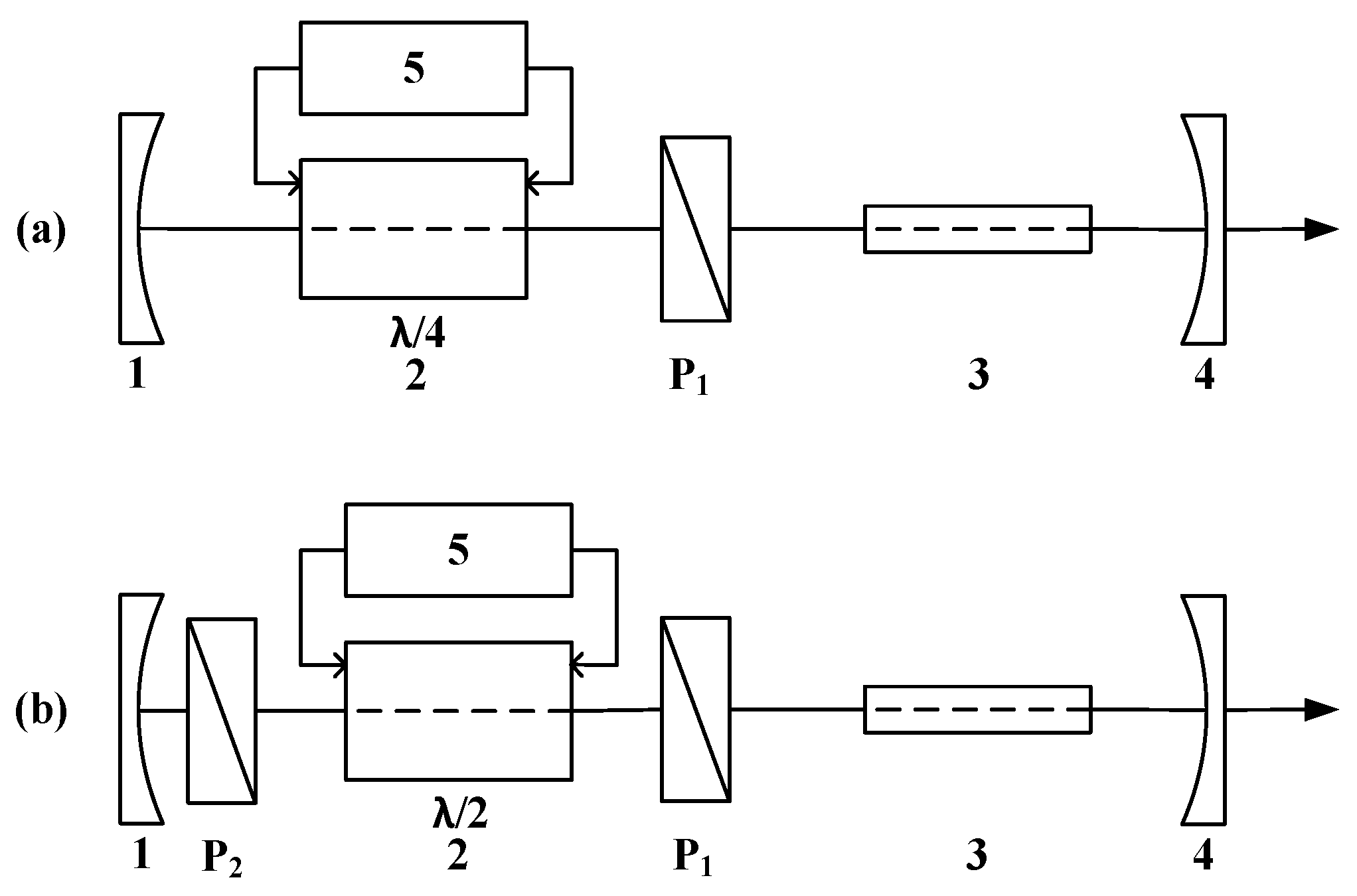
Figure 1. Two different working types of a PCD: (a) “Off-type” and (b) “On-type”. (1) Rear cavity mirror; (2) Pockels cell; (3) laser crystal; (4) output coupling cavity mirror; (5) PCD; and P 1 and P 2 : polarizers.
Photonics 10 00866 g001
Figure 2. Single-switch unipolar power supply structure.
Photonics 10 00866 g002
Figure 3. Push-pull unipolar power supply structure.
Photonics 10 00866 g003
Figure 4. Full-bridge structure: (a) unipolar power supply; (b) bipolar power supply.
Photonics 10 00866 g004
Figure 5. Push-pull circuit.
Photonics 10 00866 g005
Figure 6. Driving sequences of a push-pull circuit; (a) conventional driving sequence; (b) recharging driving sequence.
Photonics 10 00866 g006
Figure 7. Driving sequence containing dead time.
Photonics 10 00866 g007
Figure 8. Full-bridge circuit.
Photonics 10 00866 g008
Figure 9. Timing diagram of the full-bridge circuit.
Photonics 10 00866 g009
Figure 10. PWM signals with different duty cycles.
Photonics 10 00866 g010
Figure 11. Bipolar full-bridge circuit.
Photonics 10 00866 g011
Figure 12. Timing control diagram of symmetric positive and negative pulses.
Photonics 10 00866 g012
Figure 13. Timing control diagram for adjusting the pulse width.
Photonics 10 00866 g013
Figure 14. Timing control diagram of unipolar positive pulses.
Photonics 10 00866 g014
Figure 15. Timing control diagram for adjusting the pulse width.
Photonics 10 00866 g015
Figure 16. System diagram of the PCD.
Photonics 10 00866 g016
Figure 17. Timing control module.
Photonics 10 00866 g017
Figure 18. State machine of ST-P1 and ST-P2.
Photonics 10 00866 g018
Figure 19. Timing control method for generating symmetric positive and negative pulses.
Photonics 10 00866 g019
Figure 20. Diagram of the experimental setup.
Photonics 10 00866 g020
Figure 21. Short pulse with a width of 50 ns generated by S 1 and S 3 .
Photonics 10 00866 g021
Figure 22. Short pulse with a width of 50 ns generated by S 2 and S 4 .
Photonics 10 00866 g022
Figure 23. The recharging method of V P 1 .
Photonics 10 00866 g023
Figure 24. Elimination of dead time between S 1 and S 2 .
Photonics 10 00866 g024
Figure 25. High-level pulse width adjusted by a step of 10 ns.
Photonics 10 00866 g025
Figure 26. Waveforms of 50% duty cycle generated by S 1 and S 3 .
Photonics 10 00866 g026
Figure 27. Waveforms of 50% duty cycle generated by S 2 and S 4 .
Photonics 10 00866 g027
Figure 28. Low-level pulse with a width of 50 ns generated by S 1 and S 4 .
Photonics 10 00866 g028
Figure 29. Low-level pulse with a width of 50 ns generated by S 2 and S 3 .
Photonics 10 00866 g029
Figure 30. Low-level pulse width adjusted by a step size of 10 ns.
Photonics 10 00866 g030
Figure 31. Waveform with a repetition rate of 1 MHz generated by S 1 and S 3 .
Photonics 10 00866 g031
Figure 32. Waveform with a repetition rate of 1 MHz generated by S 2 and S 4 .
Photonics 10 00866 g032
Figure 33. Waveform with a repetition rate of 1 MHz and duty cycle of 1%.
Photonics 10 00866 g033
Figure 34. Waveform with a repetition rate of 1 MHz and duty cycle of 99%.
Photonics 10 00866 g034
Figure 35. Power loss of P P C , P S W , and P C T R L at operating voltage of 2.0 kV.
Photonics 10 00866 g035
Figure 36. Power efficiency of the PCD at operating voltage of 2.0 kV.
Photonics 10 00866 g036
Figure 37. Photograph of the developed PCD.
Photonics 10 00866 g037
Figure 38. Installation diagram of the PCD in a slab laser.
Photonics 10 00866 g038
Figure 39. Laser pulse generated by the slab laser.
Photonics 10 00866 g039
Table 1. Performance of different switch components.
Switching ComponentsBreakdown VoltageSwitching
Speed
Rising/Falling
Time
Complexity
Vacuum tubeshighlowmediummedium
Avalanche transistorslowmediumfasthigh
SiC MOSFETsmediumfastmediumlow
Table 2. Design specifications of the PCD.
ParametersValues
Maximum pulse voltage2.0 kV
Rising/falling time<10 ns
Maximum frequency1 MHz
Minimum pulse width10 ns
Maximum pulse widthno limitation
Adjustable pulse step10 ns
Table 3. Main parameters of C3M0350120D.
ParametersValues
Vds (br)1200 V
Vgs (th)2.5 V
Qg19 nC
Disclaimer/Publisher’s Note: The statements, opinions and data contained in all publications are solely those of the individual author(s) and contributor(s) and not of MDPI and/or the editor(s). MDPI and/or the editor(s) disclaim responsibility for any injury to people or property resulting from any ideas, methods, instructions or products referred to in the content.