Article

An Investigation of High-Performance Pressure Sensor Employing a Polymer-Defect-Based 1D Annular Photonic Crystal

by
Ayman A. Ameen
1,
Abinash Panda
2,
Ahmed Mehaney
3,*,
Abdulkarem H. M. Almawgani
4,*,
Dipika D. Pradhan
2,
Ghassan Ahmed Ali
5,
Yahya Ali Abdelrahman Ali
5 and
Hussein A. Elsayed
3
1
Physics Department, Faculty of Science, Sohag University, Sohag 82524, Egypt
2
Department of Electronics and Telecommunication Engineering, SCTR’s Pune Institute of Computer Technology, Pune 411043, India
3
Physics Department, Faculty of Science, Beni-Suef University, Beni-Suef 62512, Egypt
4
Electrical Engineering Department, College of Engineering, Najran University, Najran 66222, Saudi Arabia
5
Information Systems Department, College of Computer Sciences and Information Systems, Najran University, Najran 66222, Saudi Arabia
*
Authors to whom correspondence should be addressed.
Photonics 2023, 10(7), 731; https://doi.org/10.3390/photonics10070731
Submission received: 11 May 2023 / Revised: 12 June 2023 / Accepted: 19 June 2023 / Published: 26 June 2023
(This article belongs to the Special Issue Phononic Crystals: Science and Applications)

Abstract

:
This study aims to theoretically address the design and analysis of an efficient pressure sensor designed using a polymer-based defective 1D annular photonic crystal (APC). The 1D APC comprises an alternate arrangement of Si and SiO2 in a cylindrical fashion, incorporating a central defect layer. The investigation of the reflectance characteristics of the proposed structure is conducted by separately considering the polystyrene (PS) and the polymethyl methacrylate (PMMA) polymer materials as the defect layer. The pressure-sensitive refractive index of the polymers and the constituent materials of the APC play a vital role in envisaging the pressure-sensing application. The cornerstone of this study is represented by the shift analysis regarding the wavelength of the defect mode inside the band gap using different applied pressures, employing the modified transfer matrix method (MTMM). Various geometrical parameters like the defect polymer layer’s thickness and the APC period were carefully optimized to achieve an improved sensing performance. The proposed design demonstrated a remarkable pressure sensitivity and FoM of 51.29 nm/GPa and 301.7 GPa−1, respectively, which is considerably high in the current research scenario. It is believed that the proposed structure can be an apt candidate for an innovative high-performance pressure sensor, and could play a key role in photonic integrated circuits.

1. Introduction

Photonic crystal (PhC) is a brand-new class of optical material, which comprises a periodic arrangement of dielectric constant and can be realized in 1D, 2D, and 3D configurations [1,2,3]. In the last decade, 1D PhC attracted much attention within the scientific community because of its unique ability to control the flow of electromagnetic waves inside the crystal. The trapping of light inside the PhC structure is governed by the photonic bandgap (PBG) effect, where a particular spectral band is prohibited from propagating through the structure [4]. Remarkably, by inserting a defect layer in such a structure, its periodicity breaks, leading to the formation of strongly localized allowed states inside the PBG [5]. The PBG acts as a reflection band; therefore, the defect mode appears to be a sharp passband in the PBG. The characteristics of the defect mode can be controlled by changing the defect layer’s refractive index and thickness. This tunable property of the defect mode makes the defect-based 1D PhC the most researched topic due to its broad-ranging application domains such as sensing, filtering, waveguiding, agriculture, food safety, and bio-medical applications [6,7,8,9].
With the ongoing remarkable advances in nanotechnology, it is feasible to fabricate various geometrical configurations of PhC [10,11,12]. Recently, a new configuration of 1D PhC, known as a 1D cylindrical multilayer structure, has fascinated researchers worldwide due to its remarkable performance, particularly in sensing and filtering applications [13,14,15]. The cylindrical PhC is referred to as an annular photonic crystal (APC) or circular photonic crystal (CPC). The APC structure can be constructed by arranging alternative layers of different materials in a cylindrical ring fashion [16]. The flow of EM waves in APC was first investigated by M.A. Kaliteevkki and his team in 1999. After that, C.A. Hu et al. proposed a modified transfer matrix method (TMM) using cartesian coordinates for the analysis of transmittance and reflection characteristics of the APC [17]. Additionally, the authors thoroughly explained the fabrication feasibility of APC structure and studied the liquid sensing application. Furthermore, J. Scheuer et al. [18] introduced a ring defect into the APC structure to make annular Bragg lasers. A wide variety of materials, such as metal, dielectric, superconductor, metamaterial, etc., can be used to develop APC structures [19,20,21]. Recently, APC structures have been extensively studied for sensing applications. For example, M.M. Abadla et al. theoretically demonstrated a temperature sensor using 1D APC, where the authors studied the shift in the transmittance characteristics of the structure with a temperature rise. They achieved a significant temperature sensitivity of 0.033 nm/°C [22]. S.K. Srivastava et al. designed a 1D ternary annular PhC, where a unit cell consists of a semiconductor, superconductor, and air. The authors investigated the reflectance spectrum for both the TE and TM modes by changing the starting radius and temperature [23]. A defect-based 1D APC with a configuration of (Si/SiO2)N/2 (TiO2) (Si/SiO2)N/2 is proposed in [24]. With the help of TMM, the authors studied the transmission spectrum to analyze the shift in the defect mode frequency for varying temperatures across the defect layer. In the same vein, A. Mehany et al. designed a porous silicon-based multilayer 1D APC, where different layers contain a different percentage of porosity. The authors studied the shifting nature of the Tamm resonance mode by varying the analyte refractive index from 1 to 1.5 and achieved a remarkable sensitivity of 6770 nm/RIU [25]. S.K. Srivastava et al. designed a 1D APC by using double-negative metamaterials and studied its reflectance spectrum at different azimuthal mode numbers [26]. Similarly, S. Gandhi et al. reported a porous Si-based annular 1D PhC to detect the creatinine concentrations in blood, where they observed a maximum sensitivity of 640.29 nm/RIU and a quality factor in the order of 105. S. Jena et al. demonstrated a hydrostatic pressure sensor using different configurations of regular plannar 1D PhC [27]. In addition, F. Segovia et al. [28] and A. Herrera et al. [29] studied the shifting nature of the defect mode and band gap in relation to a rising hydrostatic pressure using plannar 1D PhC. In another related study, Liu et al. carried out an experimental investigation of the dual-core photonic crystal fiber for pressure sensing from 0 MPa to 45 MPa [28]. The regulation and detection of such a high pressure are quite difficult, which imposes a great challenge in the experimental realization of the device. Although the pressure-sensing application has been explored by using plannar 1D PhC and photonic crystal fiber, there is still plenty of improvement potential for sensing performance when investigating the effect of pressure using the APC.
Various materials can be used to create different layers and defect layers of the PhC. These materials can be semiconductors, dielecctrics, metals, superconductors, metamaterials, etc. Recently, polymer materials have emerged as a potential candidate for the design of 1D PhC owing to their exceptional tunable optical properties. By stretching and compressing the polymer materials [29,30], their properties cen be conveniently modified, with benefits in numerous applications, such as sensors, filters, and reflectors [31,32].
This study is significant piece of research as it provides a couple of novelties in the current research scenario. A thorough analysis of a novel polymer-based 1D APC is provided in the study for use in the pressure-sensing application field. The primary benefit of using a polymer material is that it has an elasto-optic effect so that the optical properties can be easily modified by applying external pressure. The mainstay of this research is to study the tunable characteristics of the defect mode with variations in pressure. Moreover, a complete optimization of different geometrical parameters was performed to achieve a remarkable sensing performance. Additionally, a 3D plot of the reflectance spectrum was studied to enhance the novelty of this study. It is believed that this work can be used as a torchbearer in the pressure-sensing application field.

2. Proposed Structure and Mathematical Modelling

The cross-sectional view of the proposed binary defect-based APC is illustrated in Figure 1. The design comprises an inner-most circular region (a starting section), which has a refractive index (RI) of n 0 and radius of γ 0 . Alternating layers of Si and SiO2 are deposited, with an RI of n 1 and n 2 , respectively, and the thicknesses are d 1 and d 2 , respectively. A defect layer of RI n d and thickness d d is inserted in the proposed APC to realize a defect mode in the transmittance spectrum. The period of APC before and after the defect layer is N 2 , where N denotes the total period of the structure. Here, the value of N is taken as 10. The entire configuration of the designed structure is ( S i / S i O 2 ) N 2 / D e f e c t / ( S i / S i O 2 ) N 2 . In this study, the proposed structure is analyzed by considering the defect layer as containing polymer materials like PS and PMMA. The outer region (the final medium) is the substrate layer, which has an RI n f .
It is assumed that the cylindrical waves emerged from the core and diverged further toward the higher layers. In the cylindrical coordinates, the Helmholtz wave equations are used to mathematically explain the E-type mode (Ez, Hϕ, H γ ), which can be written as follows [33,34]:
1 γ   γ ( γ E z γ ) + 1 γ 2 2 E z 2 = ε 0 μ 0 ϵ μ w 2 E z
By stating E z as E z = F ( r ) θ ( ) , and readjusting, we can write [22,23],
E z ( γ ,   ,   z ) = [ A W v ( q γ ) + B Z v ( q γ ) ] e i v ,
where W v and Z v   denote the first and second order of the Bessel’s function, respectively. The symbol q represents the propagation constant, which is expressed as q 2 = ε 0 μ 0 ϵ μ w 2 = k 0 2 n 2 . The tangential component is stated as follows:
H = i ω μ E z γ = i ω μ   [ A W v ( q γ ) + B Z v ( q γ ) ] e i v
To simplify the calculation, we consider only the fundamental mode (i.e., v = 0), so the simplified field equations are written as follows:
E z = [ A W 0 ( q γ ) + B Z 0 ( q γ ) ]
H = i q ω μ [ A W 1 ( q γ ) + B Z 1 ( q γ ) ] = i p = [ A W 1 ( q γ ) + B Z 1 ( q γ ) ]
The fields can be represented in a matrix form as follows [21]:
( E z H ) = ( W 0 ( q p ) Z 0 ( q p ) i p W 1 ( q p ) i p Z 1 ( q p ) ) ( A B ) ,
where p = q ω μ .   The amplitude factors A and B can be expressed as
( A B ) = ( W 0 ( q p ) Z 0 ( q p ) i p W 1 ( q p ) i p Z 1 ( q p ) ) 1 ( E z H )
By an equivalent field at γ = γ 0 is given as:
( E 0 H 0 ) γ = γ 0 = ( E 1 H 1 ) γ = γ 0 = ( W 0 ( q 1 γ 0 ) Z 0 ( q 1 γ 0 ) i p 1 W 1 ( q 1 γ 0 ) i p 1 Z 1 ( q 1 γ 0 ) ) ( A 1 B 1 )
As the amplitude remains the same within a particular layer, we can write
( A 1 B 1 ) = ( W 0 ( q 1 γ 1 ) Z 0 ( q 1 γ 1 ) i p 1 W 1 ( q 1 γ 1 ) i p 1 Z 1 ( q 1 γ 1 ) ) 1 ( E 2 H 2 ) γ = γ 1  
By inserting Equation (9) in Equation (8), we obtain
( E 0 H 0 ) γ = γ 0 = ( W 0 ( q 1 γ 0 ) Z 0 ( q 1 γ 0 ) i p 1 W 1 ( q 1 γ 0 ) i p 1 Z 1 ( q 1 γ 0 ) ) ( W 0 ( q 1 γ 1 ) Z 0 ( q 1 γ 1 ) i p 1 W 1 ( q 1 γ 1 ) i p 1 Z 1 ( q 1 γ 1 ) ) 1 ( E 2 H 2 ) γ = γ 1 = Q 1 ( E 2 H 2 ) γ = γ 1  
where Q 1 is the transfer matrix. Upon simplifying Q 1 , we can obtain the following equations:
Q 11 = π q 1 2   [ W 0 ( q 1 γ 0 ) Z 1 ( q 1 γ 1 ) W 1 ( q 1 γ 1 ) Z 0 ( q 1 γ 0 ) ]
Q 12 = i π q 1 2 p 1   [ W 0 ( q 1 γ 0 ) Z 0 ( q 1 γ 1 ) W 0 ( q 1 γ 1 ) Z 0 ( q 1 γ 0 ) ]
Q 21 = i π p 1 q 1 2   [ W 1 ( q 1 γ 0 ) Z 1 ( q 1 γ 1 ) W 1 ( q 1 γ 1 ) Z 1 ( q 1 γ 0 ) ]
Q 22 = π q 1 2   [ W 1 ( q 1 γ 0 ) Z 0 ( q 1 γ 1 ) W 0 ( q 1 γ 1 ) Z 1 ( q 1 γ 0 ) ]
By performing a similar type of analysis for other layers, the electric field at the first layer and the Nth layer can be related as
( E 0 H 0 ) γ = γ 0 = Q 1 Q 2 Q 3 Q N ( E f H f ) γ = γ N = M ( E f H f ) γ = γ N ,
where the symbol M denotes the overall transfer matrix, which can be obtained by multiplying the transfer matrix of the individual layers.

Pressure-Dependent Refractive Index of Constituent Materials

The photoelasticity effect is the method utilized to investigate the sensor’s pressure, where the material’s refractive index (RI) differs in accordance with different stress/pressure values. Specifically, the stress is associated with field components using the photoelastic constant as the fourth power of the refractive index. This variation in the RI of the material for different pressure values can be studied using a photoelastic constant. By using the photo-elasticity effect, the dependence of the refractive index on the stress effect can be expressed as follows [35]:
( 1 n 2 ) =   s a b σ b ,  
where s a b represents the strain-optic coefficient, n denotes the RI, and σ b represents the stress component. For an isotropic medium, the pressure-dependent RI can be written as [36]:
n = n 0 ( c 1 + c 2 ) σ ,  
where n 0 is the material’s RI, which corresponds to zero applied pressure; c 1 and c 2 can be specified as follows:
c 1 = n 0 3 ( s 11 2 ϑ s 12 ) 2 E
c 2 = n 0 3 [ ( s 11 ϑ ( s 11 s 12 ) ] 2 E ,  
where s 11 and s 12 signify the strain-optic coefficients, ϑ represents the Poisson’s ratio and E denotes the Young’s modulus. According to the proposed structure, the values of different constants for the materials Si, SiO2, PS, and PMMA are obtained from [37,38].

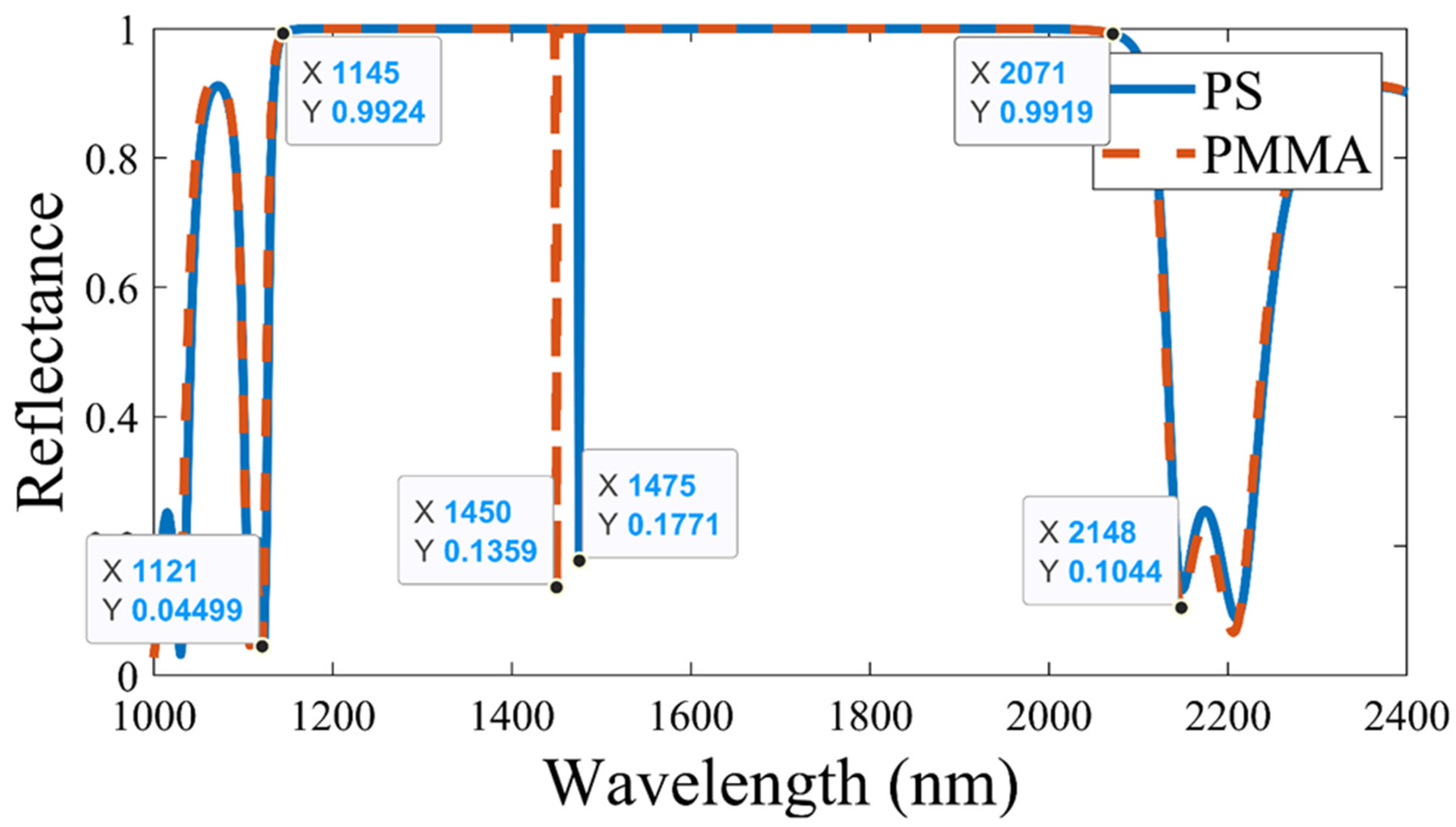
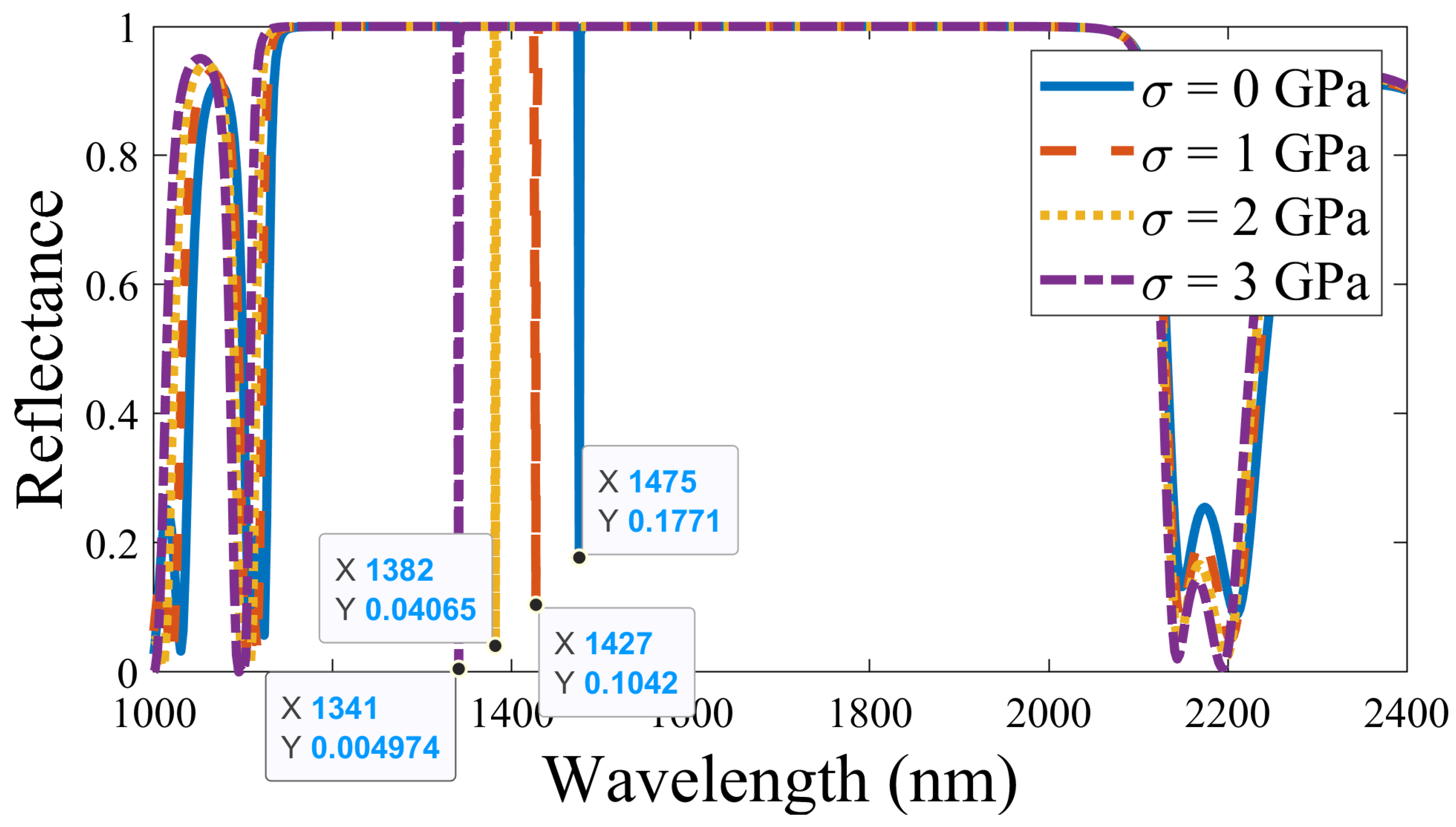
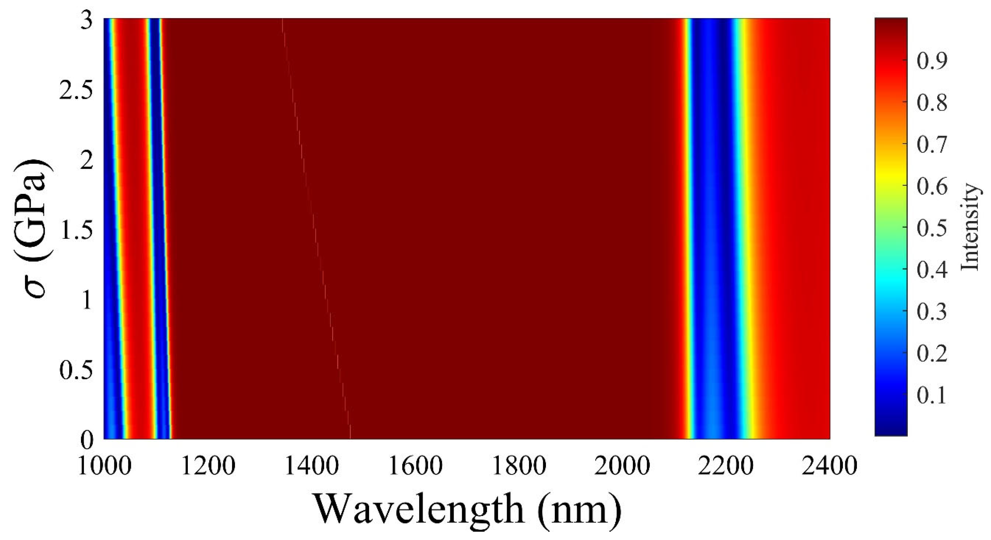
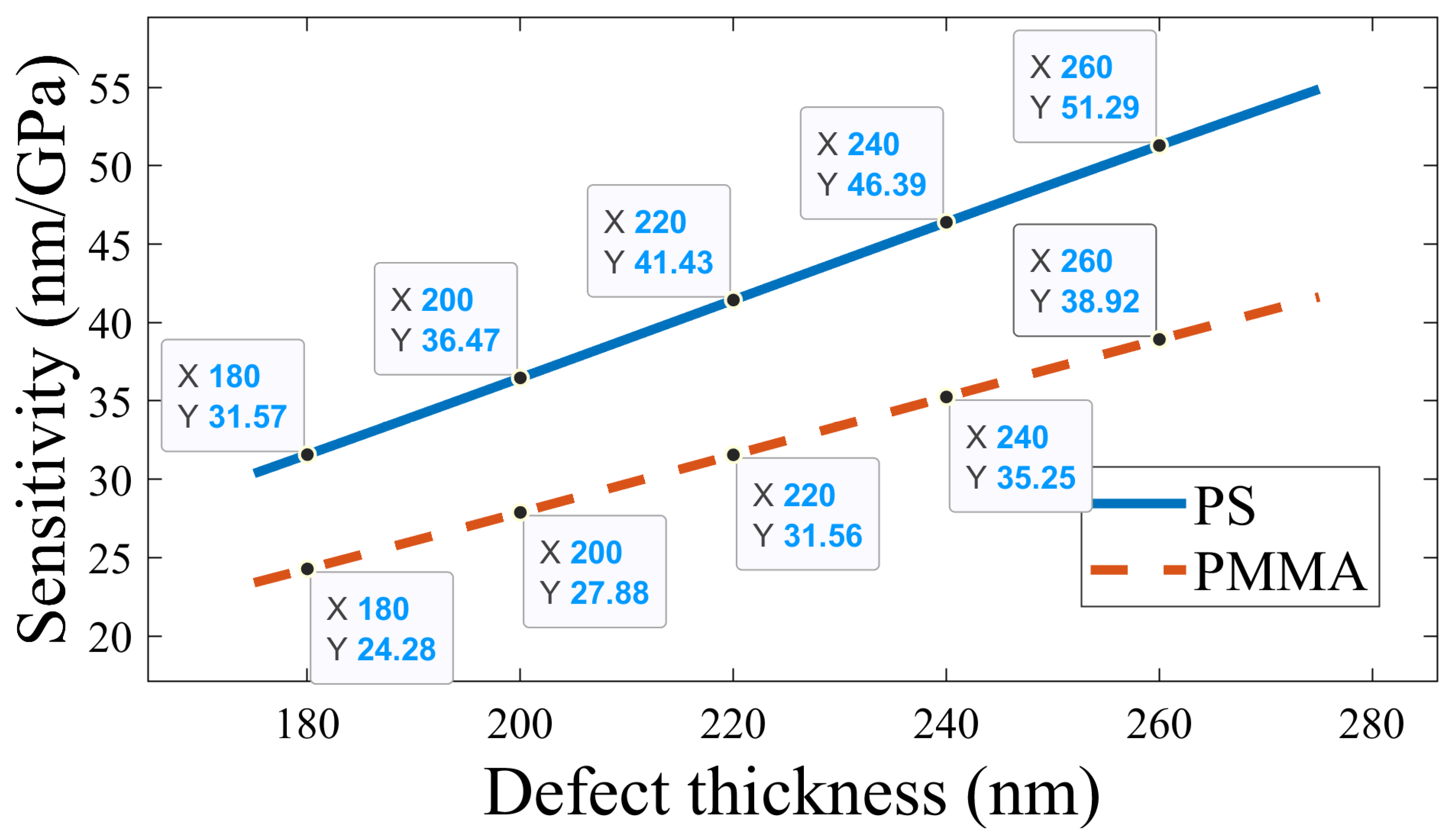
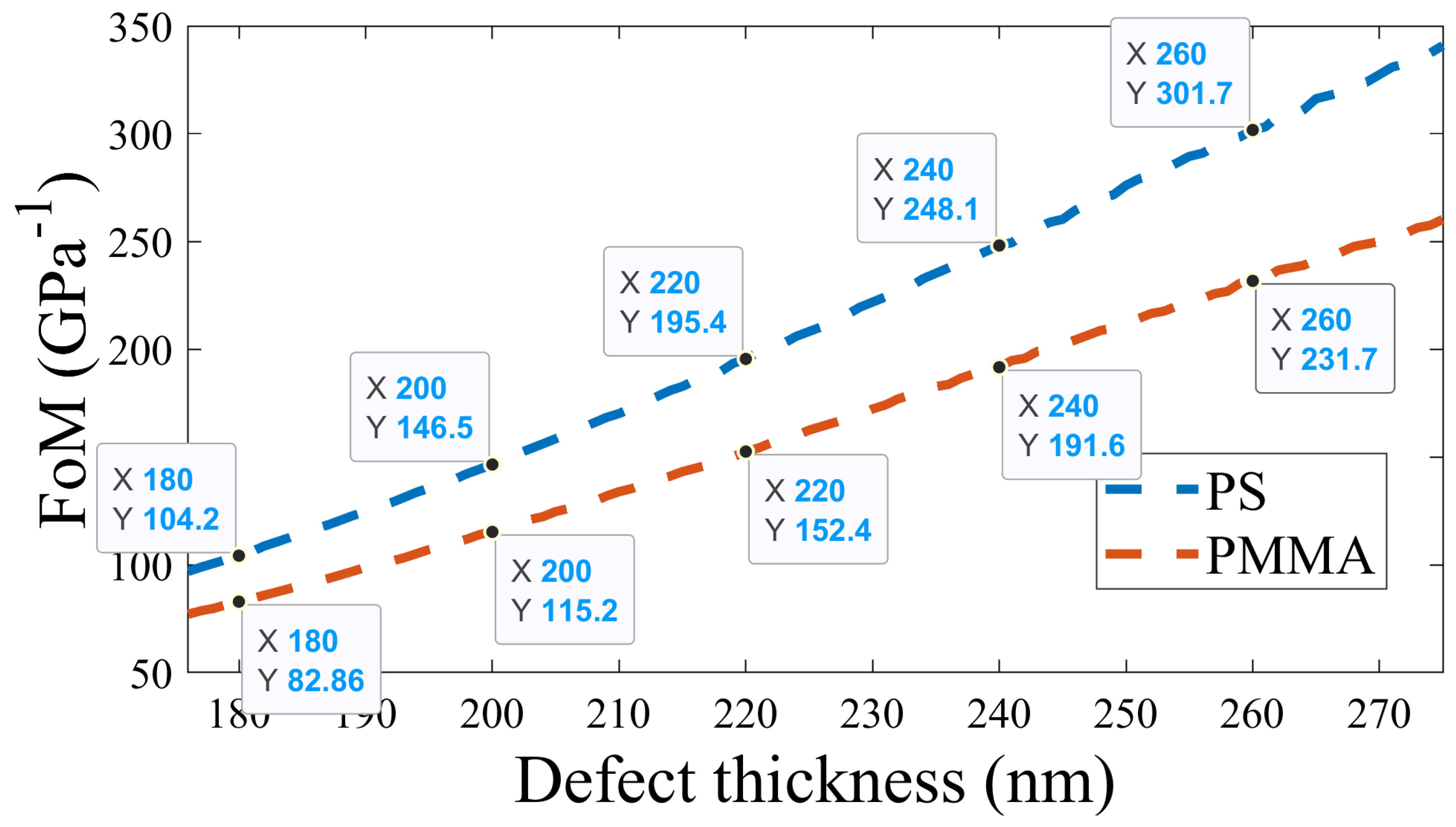
3. Results and Discussion

The suggested 1D APC was designed using the successive layers of Si and SiO2 with a period N = 10, where a defect layer is introduced in the middle of the APC. The structure was analyzed by separately considering the polymer materials (i.e., PS and PMMA) as the defect layer. Therefore, the two different proposed configurations were ( S i / S i O 2 ) N 2 / P S / ( S i / S i O 2 ) N 2 and ( S i / S i O 2 ) N 2 / P M M A / ( S i / S i O 2 ) N 2 . Here, the inclusion of the defect layer plays a promising role in the sensing and monitoring of the applied pressure. In particular, the breaking of the structure’s periodicity gives rise to the generation of a resosnant peak through the formed bandgap. This resonant mode can be tuned using the changes in the properties of the defect layer, especially its thickness and refractive index [6,9]. Therefore, the defect layer of PS or PMMA represents the mainstay of our proposed design. The refraction indices of these materials are significantly affected by the applied pressure [37,38]. The thickness of the Si and SiO2 layer was taken as d 1 = 108   nm and d 2 = 254   nm , respectively, whereas the thickness of the starting medium was γ 0 = 905   nm . The thickness of the starting medium ( γ 0 ) was considerably larger than the thickness of the constituent layers ( d 1   a n d   d 2 ) of the APC. A greater value of γ 0 confirmed that the designed APC acts analogously to the plannar 1D PhC. Initially, the thickness of the defect layer was considered to be d d = 234   nm , and the period (N) was taken as 10. Light wave incident normally on the structure, and the azimuthal number (m) was assumed to be zero to avoid computational complexity. The modified transfer matrix method (TMM) was employed to study the reflectance spectrum of the proposed APC. The polymer materials (PMMA and PS) are comparatively less rigid than the traditional semiconductor materials such as Si and SiO2. Therefore, they possess highly tunable RI characteristics concerning pressure changes.
First, the reflectance spectrum of the structure was studied by separately considering the defect layer as PS and PMMA, as shown in Figure 2. A band gap was obtained from 1145 nm to 2071 nm in the reflectance. Remarkably, a sharp dip (i.e., a defect mode) within the band gap was perceived at 1475 nm and 1450 mm for the PS and PMMA as the defect layer or layers, respectively. The mainstay of this study was to investigate the defect mode’s characteristics concerning various applied pressures across the defect layer.
Next, the pressure-sensing application of the proposed APC was analyzed by selecting PS as the defect medium. Figure 3 demonstrates the shift in the defect mode inside the band gap by increasing the pressure across the defect layer from 0 Gpa to 3 Gpa. It is observed that, with changes in the pressure, the band gap range remains fixed, whereas the defect mode position undergoes a noticeable shift. In particular, the position (wavelength) of the defect mode blue-shifted from 1475 nm to 1427 nm to 1382 nm to 1341 nm as the pressure increased from 0 GPa to 1 GPa to 2 GPa to 3 GPa, respectively. The intensity of the defect mode decreases with an increase in the applied pressure. The bandgap properties in the vicinity of the position and width were almost unaffected by the pressure variations. In contrast, the position of the defect mode significantly shifted down the shorter wavelengths with the applied increments in pressure. This response is due to the role of applied pressure on the indices of refractions of SiO2, Si and PS. The refractive index of PS showed a significant drop as the value of the applied pressure changed from 0 to 3 Gpa, unlike SiO2 and Si. Here, the refractive index of PS decreased from 1.565 to 1.074 by 0.491 due to the applied pressure [37,38]. In contrast, the changes in the indices of refraction for both SiO2 and Si did not exceed 0.029 and 0.012, respectively [39,40]. This response is due to the high values of stress optic constants of PS compared with SiO2 and Si, as previously introduced. Therefore, the dependence on PS plays a significant role in the tunability of the resonant mode, and hence its performance in the vicinity of sensitivity could be investigated.
After that, a shift in the position of the defect mode occurred with different applied pressures, considering PMMA as the defect layer. As depicted in Figure 4, the wavelength of the defect mode moved from 1450 nm to 1414 nm to 1379 nm to 1348 nm as the pressure increased from 0 GPa to 1 GPa to 2 GPa to 3 GPa, respectively. Again, the primary reason for such a shift (as shown in Figure 3 and Figure 4) in the defect mode position is that the RI of the PS and PMMA layer changes with a change in pressure, which modifies the overall transfer matrix, and results in a definite shift in the wavelength of the defect mode. This phenomenon can be explained by the following mathematical equation:
σ = m λ = n e f f ϑ ,  
where σ and ϑ denote the optical and geometrical path difference, respectively. λ represents the wavelength, n e f f is the effective refractive index, and m is an integer. When the pressure across the defect layer increases, the value of n e f f increases, causing the λ to shift toward a higher value in order to keep   σ fixed.
The variation in the position of the defect mode was plotted in relation to changes in the pressure parameter, as shown in Figure 5. It is observed that, for the PS and PMMA together as a defect layer, the defect mode wavelength decreases almost linearly with an increase in pressure. For a low pressure (0–2 MPa), the PS-based APC, the defect mode position or positions took place at relatively higher wavelength compared to the PMMA-based APC. By contrast, for high pressure (i.e., 3 MPa), the PS-based APC showed a higher defect mode wavelength than the PMMA-based APC. The fitting equation for the variation in the defect peak position for constant changes in pressure can be mathematically represented as follows:
For   PS :   λ d e f e c t = 1.94 σ 2 50.96   σ + 1476
For   PMMA :   λ d e f e c t = 1.06   σ 2 37.43   σ + 1450 ,  
where λ d e f e c t is in n m and σ is in GPa .
The variation in the intensity of the defect mode peak with changes in pressure was investigated, as shown in Figure 6. A lower-intensity defect mode value indicated that the defect mode’s position was accurately detected. As shown in the figure, for both the PS and PMMA-based APC, the intensity decreased with a rise in the applied pressure. In particular, the intensity decreased from 0.1699 to 0.104 to 0.0402 to 0.0038 for the PS-based APC and 0.1305 to 0.0825 to 0.0374 to 0.0081 for PMMA-based APC, as the pressure increased from 0 GPa to 1 GPa to 2 GPa to 3 GPa, respectively.
After that, the sensor’s sensitivity, which is the most significant parameter to assess the sensor’s performance, is calculated. The sensitivity is measured by the geometrical parameters at d 1 = 108   nm , d 2 = 254   nm , d d = 234   nm and N = 10. As depicted in Figure 7, the sensitivity of the sensor decreases with a rise in pressure. For the PS-based APC configuration, a maximum sensitivity of 49.31 nm/GPa was achieved at σ = 0 GPa, whereas for the PMMA-based APC structure, a maximum sensitivity of 36.73 nm/GPa was obtained at σ = 0 GPa. Accordingly, the significant sensitivity of the proposed structure could make it a robust candidate in the pressure-sensing application field. In addition to the pressure sensitivity, other important sensing parameters, such as quality factor, FWHM, and figure of merit for both the PS-defect-based APC and the PMMA-defect-based APC, were also computed, as illustrated in Table 1 and Table 2, respectively.
To provide a deeper understanding of the shifting nature of the defect mode, a 3D plot of the reflectance was examined, focusing on the pressure and wavelength. Figure 8 and Figure 9 represent the reflectance spectrum concerning pressure variations for PS defects and PMMA-defect-based APC, respectively. As illustrated, the blue color line indicates the lower and upper edge of the band gap. The defect mode appeared within the band gap, and the wavelength of this defect mode continued to decrease with an increase in the applied pressure. This variation is the same as the variation explained in Figure 5.
To optimize the thickness of the defect layer ( d d ), the sensitivity and FoM were computed by changing the value of d d from 180 nm to 260 nm and, when fixed, d 1 = 108   nm , d 2 = 254   nm , and N = 10. For 260 nm < d d < 180 nm, both the defect mode intensity and full-width half maximum (FWHM) are high, leading to the realization of low sensing parameters. Thus, d d is considered within the range of 180 nm and 260 nm only. For each value of d d , the sensitivity and FoM were measured for the applied pressure within the range of 0 Gpa and 3 Gpa. As shown in Figure 10, with an increase in thickness, sensitivity increases for both PS- and PMMA-defect-based APC structures. A maximum sensitivity of 51.29 nm/GPa and 38.92 nm/GPa was obtained for the PS- and PMMA-defect-based APC configurations, respectively. As shown in Figure 11, it is obvious that FoM increases with an increase in d d . The PS-defect-based APC achieved a higher FoM than the PMMA-defect-based APC structure. A maximum FoM of 326.2 1/GPa and 250.6 1/GPa was achieved for the PS- and PMMA-defect-based APC configurations, respectively. Based on the above discussion, it is confirmed that an optimum sensitivity and FoM are obtained at d d = 260   nm . Thus, the optimized value of d d is obtained as 260 nm.
Subsequently, the effect of the number of periods of APC on sensitivity and FoM is studied, as illustrated in Figure 12 and Figure 13, respectively. This simulation is carried out by setting d 1 = 108   nm and d 2 = 254   nm , d d = 260   nm , and changing the period (N) from 8 to 12. As shown in Figure 12, there is very little variation in sensitivity with an increase in the value of N. For the PS-defect-based APC, the sensitivity is significantly higher compared to the PMMA-defect-based APC. On the other hand, the value of N has a substantial impact on the FoM. As depicted in Figure 13, the FoM increases with an increase in the value of N. Like sensitivity, the PS-defect-based APC obtained superior FoM compared to the PMMA-defect-based APC. Consequently, sensitivity is the most significant sensing parameter, and it remains almost unaffected by changes in the value of N. Thus, the optimized value of N is obtained as 10.
To prove the effectiveness of the proposed sensor, we compared the obtained sensitivity with similar recently published works, which are illustrated in Table 3. The designed structure was shown to bestow the highest sensitivity. In fact, the data listed in this table show that our design could be of a significant interest as a simple, accurate and highly sensitive pressure sensor compared to its counterparts in 1D and 2D PC structures. Notably, the suggested design provides some advantages in addition its restively high sensitivity. These advantages are elucidated in the simplicity of the manufacturing procedure compared with that of 2D PC designs. In addition, the considered materials are cheaper and more common compared to other materials, such as superconductors. In this regard, we believe that the suggested design could have promising applications in a real environment.

4. Conclusions

In this study, a novel polymer-defect-based 1D annular photonic crystal sensor was designed and examined. The proposed sensor is capable of effectively sensing pressure from 0 MPa to 3 MPa. The designed structure comprises alternate layers of Si and SiO2. This structure was studied by separately considering two polymer defect layers (i.e., PS and PMMA). The modified transfer matrix method was employed to examine the reflectance characteristics of the proposed structure. The sensing principle was based on the tuning of the defect mode wavelength inside the band gap of the reflection spectra with different applied pressures. A 3D plot of the reflectance spectrum of the proposed APC was studied with pressure variations. Under the case of normal incidence, and at optimized structure parameters of d 1 = 108   nm and d 2 = 254   nm , d d = 260   nm , and N = 10, the proposed PS-defect-based APC provided a maximum sensitivity and FoM of 51.29 nm/GPa and 301.7 GPa−1, respectively. On the other hand, the PMMA-defect-based APC provided a maximum sensitivity and FoM of 38.92 nm/GPa and 231.7 GPa−1, respectively. Therefore, it is concluded that, for the designed structure, PMMA, when used as a polymer material, outperformed PS polymers in pressure-sensing applications. The fabrication feasibility and stability of the reflectance characteristics of the proposed structure made the structure designed in this study a suitable candidate for pressure-sensing applications.

Author Contributions

Project administration, A.A.A., A.P., H.A.E. and A.M.; Supervision, A.H.M.A., G.A.A., Y.A.A.A., H.A.E. and A.M.; Software, A.A.A.; Visualization, H.A.E. and A.A.A.; Writing—review and editing, H.A.E., G.A.A., Y.A.A.A., A.H.M.A. and A.M.; Writing—original draft, A.P. and D.D.P.; Methodology, A.H.M.A., G.A.A., Y.A.A.A., H.A.E. and A.A.A.; Data curation, A.A.A., A.M. and H.A.E. All authors have read and agreed to the published version of the manuscript.

Funding

The authors are thankful to the Deanship of Scientific Research at Najran University for funding this work under the Research Groups Funding program grant code (NU/RG/SERC/12/2).

Institutional Review Board Statement

Not applicable.

Informed Consent Statement

Not applicable.

Data Availability Statement

Not applicable.

Conflicts of Interest

The authors declare no conflict of interest.

References

  1. Panda, A.; Pukhrambam, P.D. Design and analysis of porous core photonic crystal fiber based ethylene glycol sensor operated at infrared wavelengths. J. Comput. Electron. 2021, 20, 943–957. [Google Scholar] [CrossRef]
  2. Li, T.; Liu, G.; Kong, H.; Yang, G.; Wei, G.; Zhou, X. Recent advances in photonic crystal-based sensors. Coord. Chem. Rev. 2023, 475, 214909. [Google Scholar] [CrossRef]
  3. Panda, A.; Pukhrambam, P.D.; Simatupang, J.W. Design of a Highly Sensitive Self-Reference Tamm-Plasmon-Polariton Sensor Employing Ti3C2Tx MXene. IEEE Sens. J. 2022, 22, 12719–12727. [Google Scholar] [CrossRef]
  4. Aly, A.H.; Sayed, F.A.; Elsayed, H.A. Defect mode tunability based on the electro-optical characteristics of the one-dimensional graphene photonic crystals. Appl. Opt. 2020, 59, 4796–4805. [Google Scholar] [CrossRef] [PubMed]
  5. Aly, A.H.; Zaky, Z.A.; Shalaby, A.S.; Ahmed, A.M.; Vigneswaran, D. Theoretical study of hybrid multifunctional one-dimensional photonic crystal as a flexible blood sugar sensor. Phys. Scr. 2020, 95, 035510. [Google Scholar] [CrossRef]
  6. Paterno, G.M.; Moscardi, L.; Donini, S.; Ariodanti, D.; Kriegel, I.; Zani, M.; Parisini, E.; Scotognella, F.; Lanzani, G. Hybrid One-Dimensional Plasmonic–Photonic Crystals for Optical Detection of Bacterial Contaminants. J. Phys. Chem. Lett. 2019, 10, 4980–4986. [Google Scholar] [CrossRef] [PubMed]
  7. Ramanujam, N.; Panda, A.; Yupapin, P.; Natesan, A.; Prabpal, P. Numerical characterization of 1D-Photonic crystal waveguide for female reproductive hormones sensing applications. Physica B 2022, 639, 414011. [Google Scholar] [CrossRef]
  8. Zaghdoudi, J.; Kanzari, M. One-dimensional photonic crystal filter using a gradient-index layer. Optik 2018, 160, 189–196. [Google Scholar] [CrossRef]
  9. Watcharakitchakorn, O.; Silapunt, R. Design and Modeling of the Photonic Crystal Waveguide Structure for Heat-Assisted Magnetic Recording. Adv. Mater. Sci. Eng. 2018, 2018, 8097841. [Google Scholar] [CrossRef] [Green Version]
  10. Devashish, D.; Ojambati, O.S.; Hasan, S.B.; van der Vegt, J.J.W.; Vos, W.L. Three dimensional photonic band gap cavity with finite support: Enhanced energy density and optical absorption. Phys. Rev. B 2019, 99, 075112. [Google Scholar] [CrossRef] [Green Version]
  11. Liu, N.; Guo, H.; Fu, L.; Kaiser, S.; Schweizer, H.; Giessen, H. Three-dimensional photonic metamaterials at optical frequencies. Nat. Mater. 2007, 7, 31–37. [Google Scholar]
  12. Yang, S.; Zhang, Y.; Peng, X.; Lu, Y.; Xie, S.; Li, J.; Chen, W.; Jiang, Z.; Peng, J.; Li, H. Theoretical study and experimental fabrication of high negative dispersion photonic crystal fiber with large area mode field. Opt. Express 2006, 14, 3015–3023. [Google Scholar] [CrossRef]
  13. Chen, M.-S.; Wu, C.-J.; Yang, T.-J. Optical properties of a superconducting annular periodic multilayer structure. Solid State Commun. 2009, 149, 1888–1893. [Google Scholar] [CrossRef]
  14. Urzhumov, Y.A.; Smith, D.R. Transformation optics with photonic band gap media. Phys. Rev. Lett. 2010, 105, 163901. [Google Scholar] [CrossRef] [PubMed] [Green Version]
  15. Erdogan, T.; King, O.; Wicks, G.W.; Hall, D.G.; Anderson, E.H.; Rooks, M.J. Circularly symmetric operation of a concentric circle grating, surface emitting, AlGaAs/GaAs quantum well semiconductor laser. Appl. Phys. Lett. 1992, 60, 1921–1923. [Google Scholar] [CrossRef]
  16. Srivastava, S.K.; Aghajamali, A. Investigation of reflectance properties in 1D ternary annular photonic crystal containing semiconductor and high-T c superconductor. J. Supercond. Nov. Magn. 2016, 29, 1423–1431. [Google Scholar] [CrossRef]
  17. Kaliteevski, M.A.; Abram, R.A.; Nikolaev, V.V.; Sokolovski, G.S. Bragg reflectors for cylindrical waves. J. Mod. Optic. 1999, 46, 875–890. [Google Scholar] [CrossRef]
  18. Scheuer, J.; Green, W.M.J.; DeRose, G.; Yariv, A. Low-threshold two-dimensional annular Bragg lasers. Optic Lett. 2004, 29, 2641. [Google Scholar] [CrossRef] [Green Version]
  19. Srivastava, S.K.; Aghajamali, A. Study of optical reflectance properties in 1D annular photonic crystal containing double negative (DNG) metamaterials. Physica B 2016, 489, 67–72. [Google Scholar] [CrossRef]
  20. Chen, M.S.; Wu, C.J.; Yang, T.J. Narrowband reflection-and-transmission filter in an annular defective photonic crystal containing an ultrathin metallic film. Opt. Commun. 2012, 285, 3143–3149. [Google Scholar] [CrossRef]
  21. El-Naggar, S.A. Properties of defect modes in cylindrical photonic crystals. Optik 2019, 200, 163447. [Google Scholar] [CrossRef]
  22. Abadla, M.M.; Elsayed, H.A.; Mehaney, A. Thermo-optical properties of binary one dimensional annular photonic crystal including temperature dependent constituents. Physica E 2020, 119, 114020. [Google Scholar] [CrossRef]
  23. Abadla, M.M.; Elsayed, H.A.; Mehaney, A. Novel Design for the Temperature Sensing Using Annular Photonic Crystals. Silicon 2021, 13, 4737–4745. [Google Scholar] [CrossRef]
  24. Mehaney, A.; Abadla, M.M.; Elsayed, H.A. 1D porous silicon photonic crystals comprising Tamm/Fano resonance as high performing optical sensors. J. Mol. Liq. 2021, 322, 114978. [Google Scholar] [CrossRef]
  25. Jena, S.; Tokas, R.; Thakur, S.; Udupa, D. Tunable mirrors and filters in 1D photonic crystals containing polymers. Physica E 2019, 114, 113627. [Google Scholar] [CrossRef]
  26. Segovia-Chaves, F.; Vinck-Posada, H. Tuning of transmittance spectrum in a one dimensional superconductor-semiconductor photonic crystal. Physica B 2018, 543, 7–13. [Google Scholar] [CrossRef]
  27. Herrera, A.Y.; Calero, J.M.; Porras-Montenegro, N. Pressure, temperature, and thickness dependence of transmittance in a 1D superconductor-semiconductor photonic crystal. J. Appl. Phys. 2018, 123, 033101. [Google Scholar] [CrossRef]
  28. Liu, Z.; Tse, M.-L.V.; Wu, C.; Chen, D.; Lu, C.; Tam, H.-Y. Intermodal coupling of supermodes in a twin-core photonic crystal fiber and its application as a pressure sensor. Opt. Express 2012, 20, 21749. [Google Scholar] [CrossRef] [Green Version]
  29. Kimura, M.; Okahara, K.; Miyamoto, T. Tunable multilayer-film distributed-Bragg-reflector filter. J. Appl. Phys. 1979, 50, 1222. [Google Scholar] [CrossRef]
  30. Kolle, M.; Zheng, B.; Gibbons, N.; Baumberg, J.J.; Steiner, U. Stretch-tuneable dielectric mirrors and optical microcavities. Opt. Express 2010, 18, 4536. [Google Scholar] [CrossRef]
  31. Krumbholz, N.; Gerlach, K.; Rutz, F.; Koch, M.; Piesiewicz, R.; Kürner, T.; Mittleman, D. Omnidirectional terahertz mirrors: A key element for future terahertz communication systems. Appl. Phys. Lett. 2006, 88, 202905. [Google Scholar] [CrossRef] [Green Version]
  32. Ghouila-Houri, C.; Gerbedoen, J.-C.; Viard, R.; Talbi, A.; Merlen, A.; Pernod, P. Design and elaboration of 1D photonic crystal cavity based on highly flexible elastomer thin layer for sensors applications. Procedia Eng. 2015, 120, 744–747. [Google Scholar] [CrossRef] [Green Version]
  33. Cheng, D.K. Field and Wave Electromagnetics; Addison Wesley Publishing Company: Toronto, ON, Canada, 1983. [Google Scholar]
  34. Chourasiaa, R.K.; Yadavb, C.S.; Upadhyayb, A.; Chourasiac, N.K.; Singhb, V. Analysis of Bragg fiber waveguides having a defect layer for biosensing applications. Opt. Int. J. Light Electron Opt. 2020, 200, 163400. [Google Scholar] [CrossRef]
  35. Katsunari, O. Fundamentals of Optical Waveguides, 2nd ed.; Academic Press: Cambridge, MA, USA, 2006. [Google Scholar]
  36. Pezzagna, S.; Brault, J.; Leroux, M.; Massies, J.; Micheli, M.D. Refractive indices and elasto-optic coefficients of GaN studied by optical waveguiding. J. Appl. Phys. 2008, 103, 123112. [Google Scholar] [CrossRef]
  37. Suthar, B.; Bhargava, A. Pressure sensor based on quantum well- structured photonic crystal. Silicon 2020, 13, 1765–1768. [Google Scholar] [CrossRef]
  38. Huang, M. Stress effects on the performance of optical waveguides. Int. J. Solid Struct. 2003, 40, 1615–1632. [Google Scholar] [CrossRef] [Green Version]
  39. Sanchez, A.; Porta, A.; Orozco, S. Photonic band-gap and defect modes of a one-dimensional photonic crystal under localized compression. J. Appl. Phys. 2017, 121, 173101. [Google Scholar] [CrossRef]
  40. Dinodiya, S.; Bhargava, A. A Comparative Analysis of Pressure Sensing Parameters for Two Dimensional Photonic Crystal Sensors Based on Si and GaAs. Silicon 2021, 14, 4611–4618. [Google Scholar] [CrossRef]
  41. Rajasekar, R.; Robinson, S. Nano-pressure and temperature sensor based on hexagonal photonic crystal ring resonator. Plasmonics 2019, 14, 3–15. [Google Scholar] [CrossRef]
  42. MiShra, C.S.; Das, S.; Nayak, M.R.; PukhraMbaM, P.D.; Panda, A.; Palai, G. Towards a Highly Sensitive Pressure Sensor Using an Infrared (IR) Laser and a Two-dimensional (2-D) Photonic Crystal Waveguide. Lasers Eng. 2022, 53, 105–119. [Google Scholar]
  43. Ben-Ali, Y.; Elamri, F.Z.; Ouariach, A.; Falyouni, F.; Tahri, Z.; Bria, D. A high sensitivity hydrostatic pressure and temperature based on a defective 1D photonic crystal. J. Electromagn. Waves Appl. 2020, 34, 2030–2050. [Google Scholar] [CrossRef]
  44. Thara, R.L.; Priya, P.A.; Nayak, C. Pressure Dependent Characteristics of 1D Random Photonic. J. Phys. Conf. Ser. 2022, 2335, 012013. [Google Scholar]
  45. Sabra, W.; Elsayed, H.A.; Mehaney, A.; Aly, A.H. Numerical optimization of 1D superconductor photonic crystals pressure sensor for low temperatures applications. Solid State Commun. 2022, 343, 114671. [Google Scholar] [CrossRef]
Figure 1. Schematic of the proposed annular photonic crystal (APC).
Photonics 10 00731 g001
Figure 2. Reflectance spectrum of Si/SiO2 annular photonic crystal with PS and PMMA as the defect layers.
Photonics 10 00731 g002
Figure 3. Reflectance of the annular photonic crystal with PS as a defect layer at different pressures.
Photonics 10 00731 g003
Figure 4. Reflectance of the annular photonic crystal with PMMA as a defect layer at different pressures.
Photonics 10 00731 g004
Figure 5. Variation in the defect peak positions with pressure variation.
Photonics 10 00731 g005
Figure 6. Variation in the intensity of the defect peak with pressure variations.
Photonics 10 00731 g006
Figure 7. Analysis of pressure sensitivity of two annular photonic crystals with defects in PS and PMMA.
Photonics 10 00731 g007
Figure 8. Reflectance of the APC with PS as a defect layer with pressure variation.
Photonics 10 00731 g008
Figure 9. Reflectance with PMMA as a defect layer for APC with pressure variation.
Photonics 10 00731 g009
Figure 10. Variations in sensitivity with changes in the defect layer thickness; sensitivity is measured between 0 GPa and 3 GPa.
Photonics 10 00731 g010
Figure 11. Changes in the figure of merit with changes in the defect layer thickness.
Photonics 10 00731 g011
Figure 12. Variations in sensitivity with changes in the periodicity number; sensitivity is measured between 0 GPa and 3 Gpa.
Photonics 10 00731 g012
Figure 13. Variations in the figure of merit with changes in the periodicity number.
Photonics 10 00731 g013
Table 1. Evaluation of the sensor’s performance parameters for the PS-defect-based APC.
Pressure   ( G P a ) Defect   Peak   Position   ( n m ) Defect Peak Intensity Sensitivity
( n m / G P a )
FWHM   ( n m ) Quality Factor Figure of Merit
( G P a 1 )
01475.40.177N/A0.2346305.1N/A
11427.00.10448.40.2046994.9237.5
21381.50.04046.90.1927195.5244.4
31340.70.00444.90.1936946.5232.7
Table 2. Evaluation of the sensor’s performance parameters for the PMMA-defect-based APC.
Pressure   ( G P a ) Defect   Peak   Position   ( n m ) Defect Peak Intensity Sensitivity
( n m / G P a )
FWHM   ( n m ) Quality Factor Figure of Merit
( G P a 1 )
01449.90.135N/A0.2246473.0N/A
11413.80.08336.10.2036964.6178.0
21379.50.03735.20.1927184.7183.6
31347.50.00834.10.1907092.2179.7
Table 3. Comparative analysis of sensing performance.
Sl. No.Structure ConfigurationSensitivity (nm/GPa)Reference
1Si/GaAs-based 2D PhC17[39]
2Ring-resonator-based 2D PhC10[40]
3InAs/ZnO-based 2D PhC75[41]
41D PhC of SiO2-TiO2 with GaAs defect8.6[42]
5Quantum-well-based PhC6.74[43]
61D PhC with polymer defect35[44]
7Superconductor-based 1D PhC1.7467[45]
81D APC with polymer defect layer51.29 nm/GPaThis research
Disclaimer/Publisher’s Note: The statements, opinions and data contained in all publications are solely those of the individual author(s) and contributor(s) and not of MDPI and/or the editor(s). MDPI and/or the editor(s) disclaim responsibility for any injury to people or property resulting from any ideas, methods, instructions or products referred to in the content.

