Tamm Plasmons in TiO2 Nanotube Photonic Crystals

 ,
,  ,
,  , , and
Abstract
1. Introduction
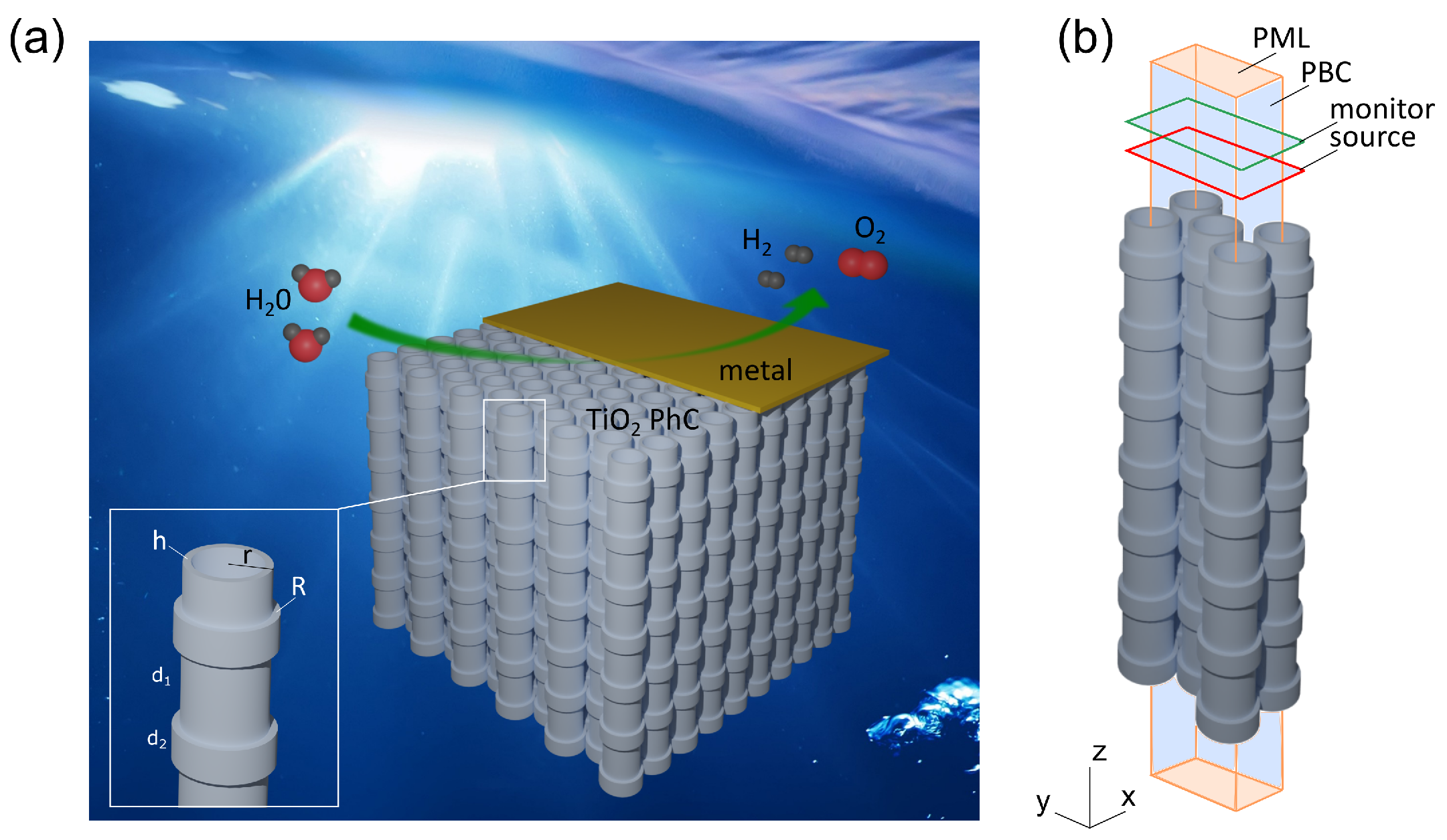
2. Structure Design
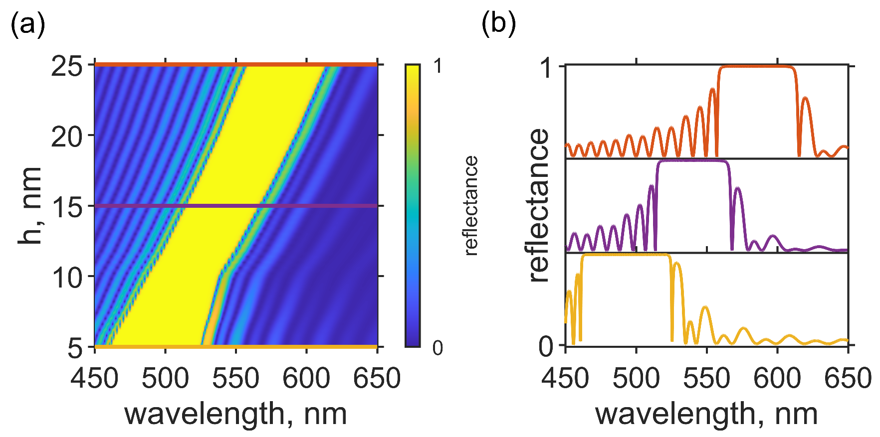
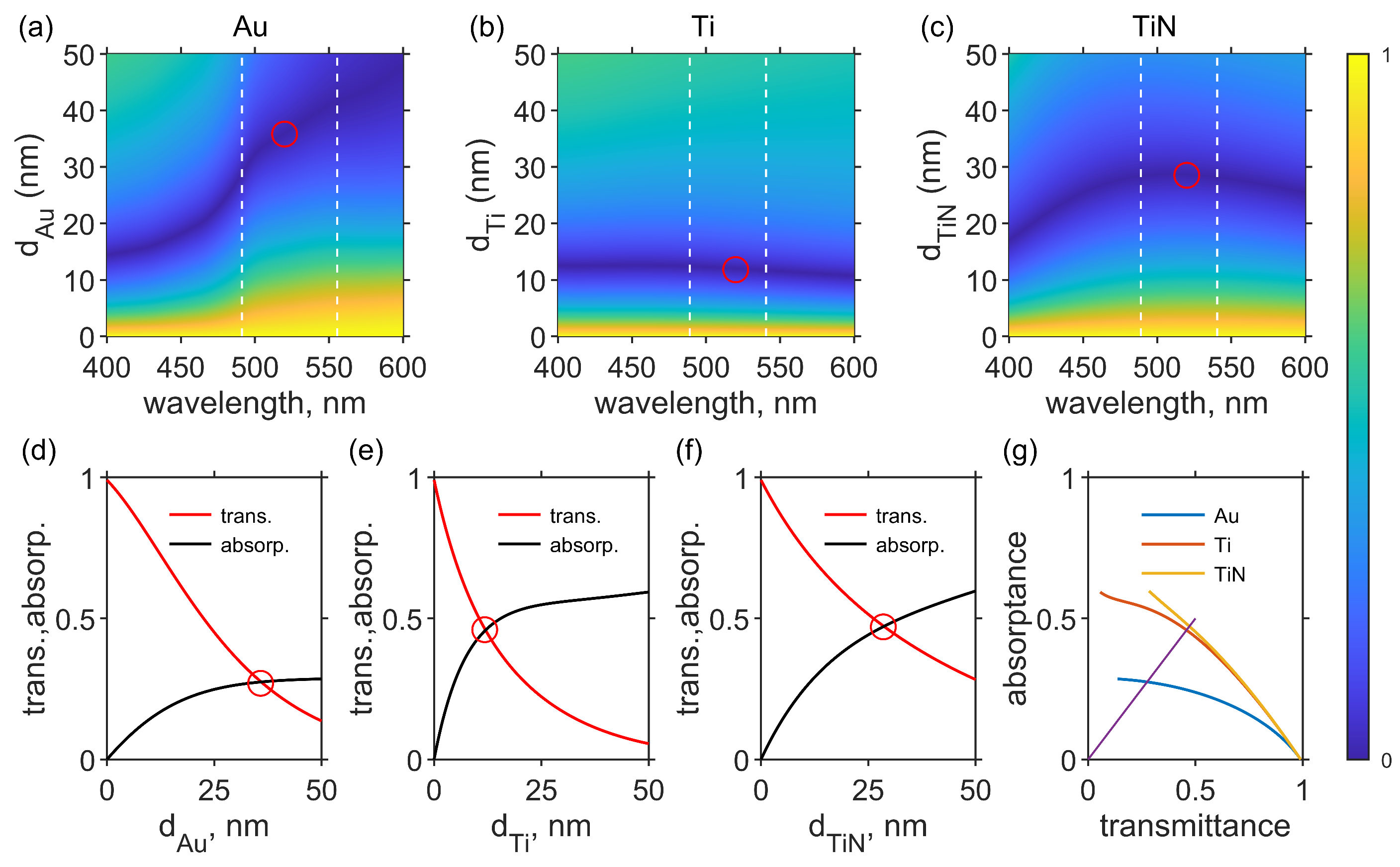
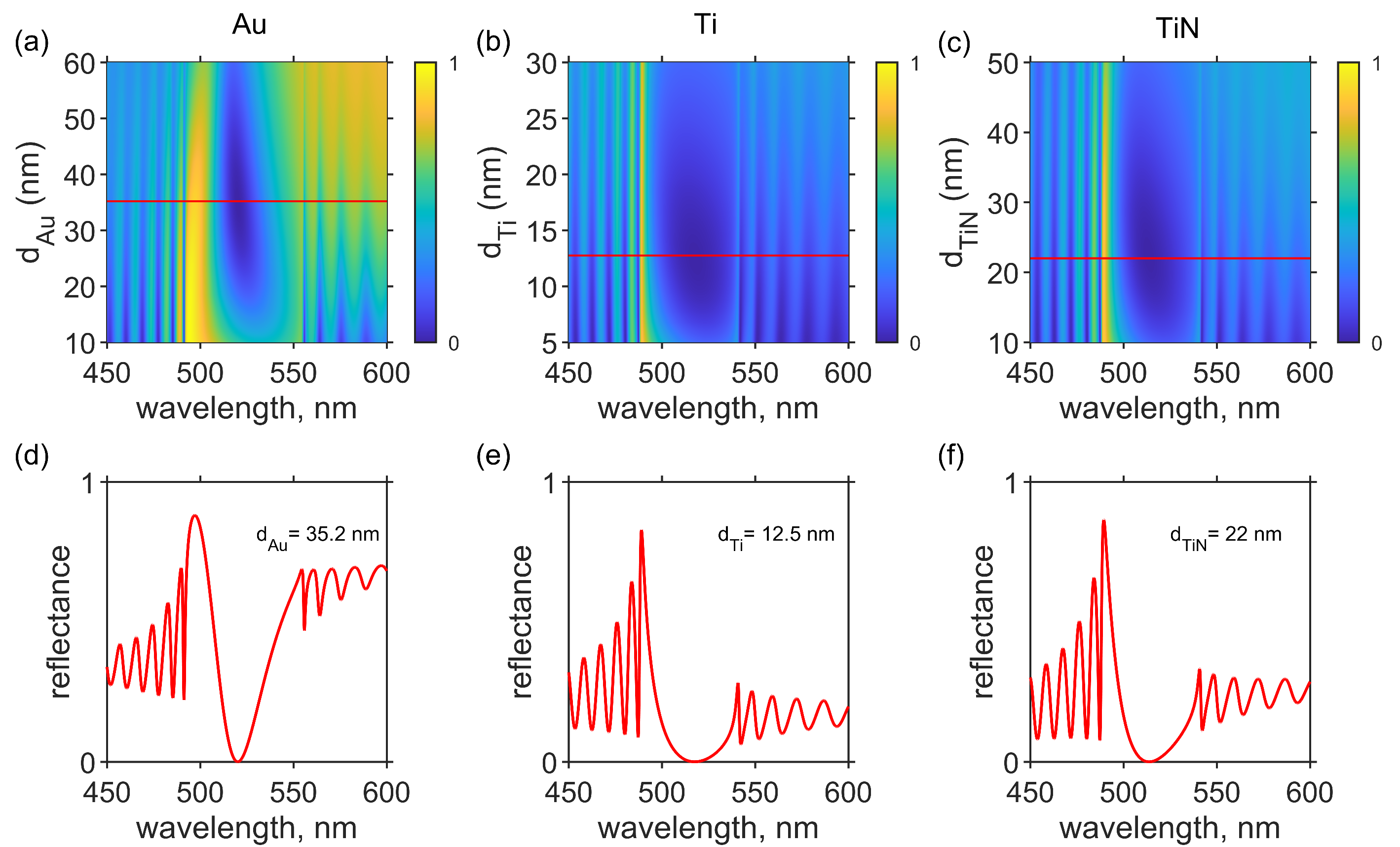
3. Results and Discussion
4. Conclusions
Author Contributions
Funding
Institutional Review Board Statement
Informed Consent Statement
Data Availability Statement
Conflicts of Interest
References
- Kavokin, A.V.; Shelykh, I.A.; Malpuech, G. Lossless interface modes at the boundary between two periodic dielectric structures. Phys. Rev. B 2005, 72, 233102. [Google Scholar] [CrossRef]
- Vinogradov, A.P.; Dorofeenko, A.V.; Erokhin, S.G.; Inoue, M.; Lisyansky, A.A.; Merzlikin, A.M.; Granovsky, A.B. Surface state peculiarities in one-dimensional photonic crystal interfaces. Phys. Rev. B 2006, 74, 045128. [Google Scholar] [CrossRef]
- Kaliteevski, M.; Iorsh, I.; Brand, S.; Abram, R.A.; Chamberlain, J.M.; Kavokin, A.V.; Shelykh, I.A. Tamm plasmon-polaritons: Possible electromagnetic states at the interface of a metal and a dielectric Bragg mirror. Phys. Rev. B 2007, 76, 165415. [Google Scholar] [CrossRef]
- Sasin, M.; Seisyan, R.; Kalitteevski, M.; Brand, S.; Abram, R.; Chamberlain, J.; Egorov, A.Y.; Vasil’Ev, A.; Mikhrin, V.; Kavokin, A. Tamm plasmon polaritons: Slow and spatially compact light. Appl. Phys. Lett. 2008, 92, 251112. [Google Scholar] [CrossRef]
- Goto, T.; Dorofeenko, A.V.; Merzlikin, A.M.; Baryshev, A.V.; Vinogradov, A.P.; Inoue, M.; Lisyansky, A.A.; Granovsky, A.B. Optical Tamm States in One-Dimensional Magnetophotonic Structures. Phys. Rev. Lett. 2008, 101, 113902. [Google Scholar] [CrossRef]
- Chen, H.; Chen, Z.; Yang, H.; Wen, L.; Yi, Z.; Zhou, Z.; Dai, B.; Zhang, J.; Wu, X.; Wu, P. Multi-mode surface plasmon resonance absorber based on dart-type single-layer graphene. RSC Adv. 2022, 12, 7821–7829. [Google Scholar] [CrossRef]
- Deng, Y.; Cao, G.; Wu, Y.; Zhou, X.; Liao, W. Theoretical description of dynamic transmission characteristics in MDM waveguide aperture-side-coupled with ring cavity. Plasmonics 2015, 10, 1537–1543. [Google Scholar] [CrossRef]
- Pankin, P.S.; Sutormin, V.S.; Gunyakov, V.A.; Zelenov, F.V.; Tambasov, I.A.; Masyugin, A.N.; Volochaev, M.N.; Baron, F.A.; Chen, K.P.; Zyryanov, V.Y.; et al. Experimental implementation of tunable hybrid Tamm-microcavity modes. Appl. Phys. Lett. 2021, 119, 161107. [Google Scholar] [CrossRef]
- Huang, S.G.; Chen, K.P.; Jeng, S.C. Phase sensitive sensor on Tamm plasmon devices. Opt. Mater. Express 2017, 7, 1267–1273. [Google Scholar] [CrossRef]
- Buchnev, O.; Belosludtsev, A.; Reshetnyak, V.; Evans, D.R.; Fedotov, V.A. Observing and controlling a Tamm plasmon at the interface with a metasurface. Nanophotonics 2020, 9, 897–903. [Google Scholar] [CrossRef]
- Chen, J.; Zhang, Q.; Peng, C.; Tang, C.; Shen, X.; Deng, L.; Park, G.S. Optical Cavity-Enhanced Localized Surface Plasmon Resonance for High-Quality Sensing. IEEE Photonics Technol. Lett. 2018, 30, 728–731. [Google Scholar] [CrossRef]
- Thompson, R.J.; Siday, T.; Glass, S.; Luk, T.S.; Reno, J.L.; Brener, I.; Mitrofanov, O. Optically thin hybrid cavity for terahertz photo-conductive detectors. Appl. Phys. Lett. 2017, 110, 041105. [Google Scholar] [CrossRef]
- Zhang, W.L.; Wang, F.; Rao, Y.J.; Jiang, Y. Novel sensing concept based on optical Tamm plasmon. Opt. Express 2014, 22, 14524–14529. [Google Scholar] [CrossRef]
- Jeng, S.C. Applications of Tamm plasmon-liquid crystal devices. Liq. Cryst. 2020, 47, 1223–1231. [Google Scholar] [CrossRef]
- Wang, L.; Cai, W.; Bie, M.; Zhang, X.; Xu, J. Zak phase and topological plasmonic Tamm states in one-dimensional plasmonic crystals. Opt. Express 2018, 26, 28963–28975. [Google Scholar] [CrossRef] [PubMed]
- Lakhtakia, A.; McCall, M. Sculptured thin films as ultranarrow-bandpass circular-polarization filters. Opt. Commun. 1999, 168, 457–465. [Google Scholar] [CrossRef]
- Zhou, W.; Dridi, M.; Suh, J.Y.; Kim, C.H.; Co, D.T.; Wasielewski, M.R.; Schatz, G.C.; Odom, T.W. Lasing action in strongly coupled plasmonic nanocavity arrays. Nat. Nanotechnol. 2013, 8, 506–511. [Google Scholar] [CrossRef]
- Symonds, C.; Lheureux, G.; Hugonin, J.P.; Greffet, J.J.; Laverdant, J.; Brucoli, G.; Lemaitre, A.; Senellart, P.; Bellessa, J. Confined Tamm Plasmon Lasers. Nano Lett. 2013, 13, 3179–3184. [Google Scholar] [CrossRef]
- Fang, M.; Shi, F.; Chen, Y. Unidirectional all-optical absorption switch based on optical Tamm state in nonlinear plasmonic waveguide. Plasmonics 2016, 11, 197–203. [Google Scholar] [CrossRef]
- Bikbaev, R.G.; Vetrov, S.Y.; Timofeev, I.V. Epsilon-Near-Zero Absorber by Tamm Plasmon Polariton. Photonics 2019, 6, 28. [Google Scholar] [CrossRef]
- Pühringer, G.; Consani, C.; Jannesari, R.; Fleury, C.; Dubois, F.; Spettel, J.; Dao, T.D.; Stocker, G.; Grille, T.; Jakoby, B. Design of a Slab Tamm Plasmon Resonator Coupled to a Multistrip Array Waveguide for the Mid Infrared. Sensors 2022, 22, 2968. [Google Scholar] [CrossRef] [PubMed]
- Zhang, X.L.; Song, J.F.; Li, X.B.; Feng, J.; Sun, H.B. Optical Tamm states enhanced broad-band absorption of organic solar cells. Appl. Phys. Lett. 2012, 101, 243901. [Google Scholar] [CrossRef]
- Bikbaev, R.G.; Vetrov, S.Y.; Timofeev, I.V.; Shabanov, V.F. Photosensitivity and reflectivity of the active layer in a Tamm-plasmon-polariton-based organic solar cell. Appl. Opt. 2021, 60, 3338–3343. [Google Scholar] [CrossRef] [PubMed]
- Vyunishev, A.M.; Bikbaev, R.G.; Svyakhovskiy, S.E.; Timofeev, I.V.; Pankin, P.S.; Evlashin, S.A.; Vetrov, S.Y.; Myslivets, S.A.; Arkhipkin, V.G. Broadband Tamm plasmon polariton. J. Opt. Soc. Am. B 2019, 36, 2299–2305. [Google Scholar] [CrossRef]
- Pyatnov, M.V.; Bikbaev, R.G.; Timofeev, I.V.; Ryzhkov, I.I.; Vetrov, S.Y.; Shabanov, V.F. Broadband Tamm Plasmons in Chirped Photonic Crystals for Light-Induced Water Splitting. Nanomaterials 2022, 12, 928. [Google Scholar] [CrossRef]
- Eliseev, A.A.; Lukashin, A.V. Funtional’nye Nanomaterialy (Functional Nanomaterials); Fizmatlit: Moscow, Russia, 2010; p. 456. [Google Scholar]
- Bobrovsky, A.Y.; Svyakhovskiy, S.; Roslyakov, I.V.; Piryazev, A.A.; Ivanov, D.A.; Shibaev, V.P.; Cigl, M.; Hamplová, V.; Bubnov, A. Photoinduced Split of the Cavity Mode in Photonic Crystals Based on Porous Silicon Filled with Photochromic Azobenzene-Containing Substances. ACS Appl. Pol. Mat. 2022, 4, 7387–7396. [Google Scholar] [CrossRef]
- Law, C.S.; Lim, S.Y.; Abell, A.D.; Voelcker, N.H.; Santos, A. Nanoporous anodic alumina photonic crystals for optical chemo-and biosensing: Fundamentals, advances, and perspectives. Nanomaterials 2018, 8, 788. [Google Scholar] [CrossRef]
- Roy, P.; Berger, S.; Schmuki, P. TiO2 Nanotubes: Synthesis and Applications. Angew. Chem. Int. Ed. 2011, 50, 2904–2939. [Google Scholar] [CrossRef]
- Ermolaev, G.A.; Kushnir, S.E.; Sapoletova, N.A.; Napolskii, K.S. Titania photonic crystals with precise photonic band gap position via anodizing with voltage versus optical path length modulation. Nanomaterials 2019, 9, 651. [Google Scholar] [CrossRef]
- Sadykov, A.; Kushnir, S.; Sapoletova, N.; Ivanov, V.; Napolskii, K. Anodic titania photonic crystals with high reflectance within photonic band gap via pore shape engineering. Scr. Mater. 2020, 178, 13–17. [Google Scholar] [CrossRef]
- Li, J.F.; Wang, J.; Wang, X.T.; Wang, X.G.; Li, Y.; Wang, C.W. Bandgap engineering of TiO2 nanotube photonic crystals for enhancement of photocatalytic capability. CrystEngComm 2020, 22, 1929–1938. [Google Scholar] [CrossRef]
- Guo, M.; Xie, K.; Wang, Y.; Zhou, L.; Huang, H. Aperiodic TiO2 nanotube photonic crystal: Full-visible-spectrum solar light harvesting in photovoltaic devices. Sci. Rep. 2014, 4, 6442. [Google Scholar] [CrossRef] [PubMed]
- Guo, M.; Su, H.; Zhang, J.; Liu, L.; Fu, N.; Yong, Z.; Huang, H.; Xie, K. Broadband and omnidirectional light harvesting enhancement in photovoltaic devices with aperiodic TiO2 nanotube photonic crystal. J. Power Sources 2017, 345, 12–20. [Google Scholar] [CrossRef]
- Golovan, L.A.; Timoshenko, V.Y.; Kashkarov, P.K. Optical properties of porous-system-based nanocomposites. Physics-Uspekhi 2007, 50, 595. [Google Scholar] [CrossRef]
- Johnson, P.B.; Christy, R.W. Optical Constants of the Noble Metals. Phys. Rev. B 1972, 6, 4370–4379. [Google Scholar] [CrossRef]
- Palik, E.D. Handbook of Optical Constants of Solids; Academic Press: Boca Raton, FL, USA, 2014. [Google Scholar]
- Haus, H. Waves and Fields in Optoelectronics; Prentice-Hall, Inc.: Englewood Cliffs, NJ, USA, 1984; p. 402. [Google Scholar]
- John, S.; Joannopoulos, D.; Winn, J.N.; Meade, R.D. Photonic Crystals: Molding the Flow of Light; Princeton University of Press: Princeton, NJ, USA, 2008. [Google Scholar]
- Yang, Z.Y.; Ishii, S.; Yokoyama, T.; Dao, T.D.; Sun, M.G.; Pankin, P.S.; Timofeev, I.V.; Nagao, T.; Chen, K.P. Narrowband Wavelength Selective Thermal Emitters by Confined Tamm Plasmon Polaritons. ACS Photonics 2017, 4, 2212–2219. [Google Scholar] [CrossRef]


| Symbol | Structural Parameter | Value |
|---|---|---|
| L | TiO nanotube length | 6 m |
| r | Outer radius | 55 nm |
| h | Wall thickness | 10 nm |
| R | Outer radius of ring thickenings | 65 nm |
| d | Distance between rings | 105 nm |
| d | Height of ring thickenings | 45 nm |
| d | Metallic layer thickness |
| Metal | Thickness Defined by TCMT | Thickness Defined by Transfer Matrix |
|---|---|---|
| Au | 35.8 nm | 35.2 nm |
| Ti | 11.2 nm | 12.5 nm |
| TiN | 28 nm | 22 nm |
Disclaimer/Publisher’s Note: The statements, opinions and data contained in all publications are solely those of the individual author(s) and contributor(s) and not of MDPI and/or the editor(s). MDPI and/or the editor(s) disclaim responsibility for any injury to people or property resulting from any ideas, methods, instructions or products referred to in the content. |
© 2023 by the authors. Licensee MDPI, Basel, Switzerland. This article is an open access article distributed under the terms and conditions of the Creative Commons Attribution (CC BY) license (https://creativecommons.org/licenses/by/4.0/).
Share and Cite
Pyatnov, M.V.; Bikbaev, R.G.; Timofeev, I.V.; Ryzhkov, I.I.; Vetrov, S.Y.; Shabanov, V.F. Tamm Plasmons in TiO2 Nanotube Photonic Crystals. Photonics 2023, 10, 64. https://doi.org/10.3390/photonics10010064
Pyatnov MV, Bikbaev RG, Timofeev IV, Ryzhkov II, Vetrov SY, Shabanov VF. Tamm Plasmons in TiO2 Nanotube Photonic Crystals. Photonics. 2023; 10(1):64. https://doi.org/10.3390/photonics10010064
Chicago/Turabian StylePyatnov, Maxim V., Rashid G. Bikbaev, Ivan V. Timofeev, Ilya I. Ryzhkov, Stepan Ya. Vetrov, and Vasily F. Shabanov. 2023. "Tamm Plasmons in TiO2 Nanotube Photonic Crystals" Photonics 10, no. 1: 64. https://doi.org/10.3390/photonics10010064
APA StylePyatnov, M. V., Bikbaev, R. G., Timofeev, I. V., Ryzhkov, I. I., Vetrov, S. Y., & Shabanov, V. F. (2023). Tamm Plasmons in TiO2 Nanotube Photonic Crystals. Photonics, 10(1), 64. https://doi.org/10.3390/photonics10010064