Reduction in Crosstalk between Integrated Anisotropic Optical Waveguides

 , , ,
, , ,  and
and 
Abstract
1. Introduction
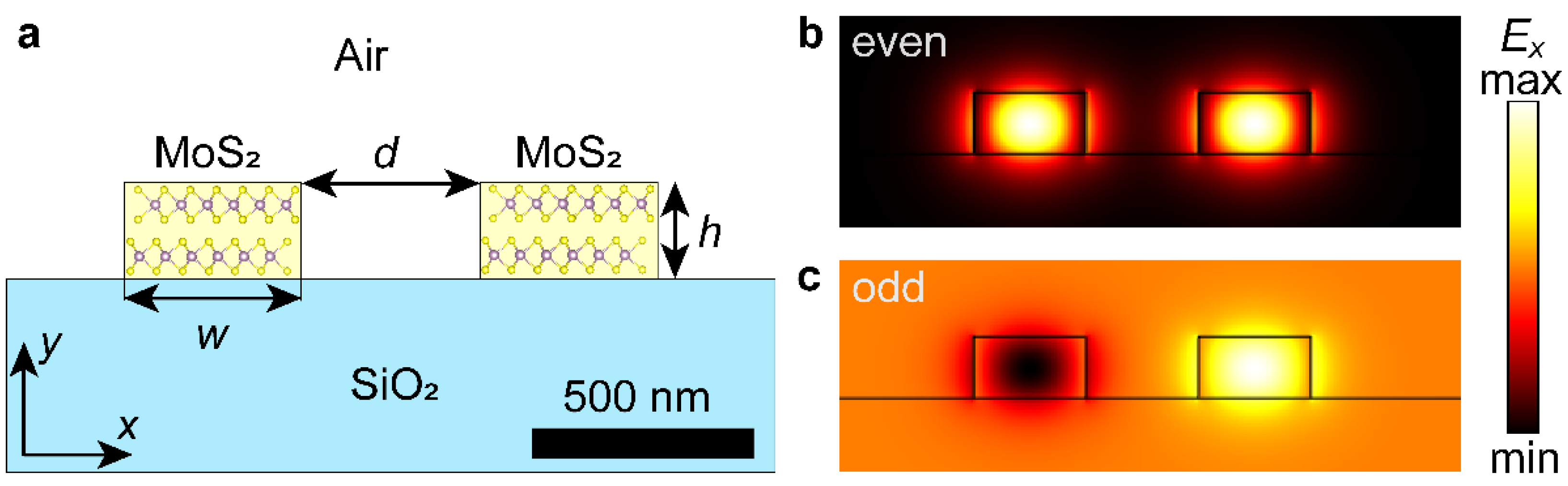
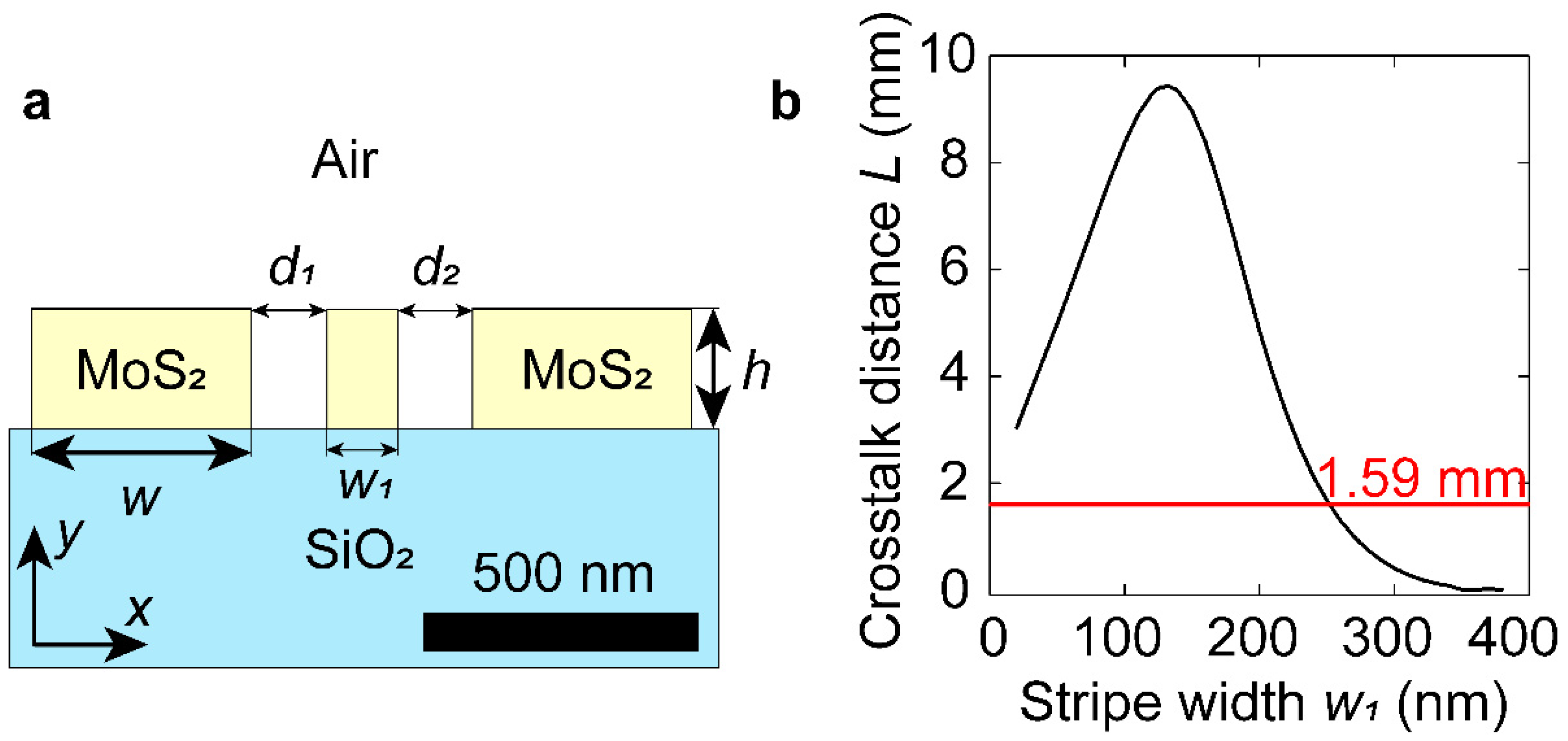
2. Results
3. Discussion
Author Contributions
Funding
Data Availability Statement
Conflicts of Interest
Appendix A

References
- Atabaki, A.H.; Moazeni, S.; Pavanello, F.; Gevorgyan, H.; Notaros, J.; Alloatti, L.; Wade, M.T.; Sun, C.; Kruger, S.A.; Meng, H.; et al. Integrating Photonics with Silicon Nanoelectronics for the next Generation of Systems on a Chip. Nature 2018, 556, 349. [Google Scholar] [CrossRef] [PubMed]
- Bogaerts, W.; Pérez, D.; Capmany, J.; Miller, D.A.B.; Poon, J.; Englund, D.; Morichetti, F.; Melloni, A. Programmable photonic circuits. Nature 2020, 586, 207. [Google Scholar] [CrossRef] [PubMed]
- Tanaka, Y. Recent Progress in the Development of Large-Capacity Integrated Silicon Photonics Transceivers. IEICE Trans. Electron. 2019, E102.C, 357. [Google Scholar] [CrossRef]
- Margalit, N.; Xiang, C.; Bowers, S.M.; Bjorlin, A.; Blum, R.; Bowers, J.E. Perspective on the future of silicon photonics and electronics. Appl. Phys. Lett. 2021, 118, 220501. [Google Scholar] [CrossRef]
- Zhang, J.; Shi, X.; Zhang, Z.; Guo, K.; Yang, J. Ultra-compact, efficient and high-polarization-extinction-ratio polarization beam splitters based on photonic anisotropic metamaterials. Opt. Express 2022, 30, 538–549. [Google Scholar] [CrossRef]
- Shi, X.; Zhang, J.; Fan, W.; Lu, Y.; Peng, N.; Rottwitt, K.; Ou, H. Compact low-birefringence polarization beam splitter using vertical-dual-slot waveguides in silicon carbide integrated platforms. Photonics Res. 2022, 10, A8–A13. [Google Scholar] [CrossRef]
- Su, L.; Piggott, A.Y.; Sapra, N.V.; Petykiewicz, J.; Vučković, J. Inverse Design and Demonstration of a Compact on-Chip Narrowband Three-Channel Wavelength Demultiplexer. ACS Photonics 2018, 5, 301. [Google Scholar] [CrossRef]
- Lu, J.; Vuckovic, J. Nanophotonic computational design. Opt. Express 2013, 21, 13351. [Google Scholar] [CrossRef]
- Huang, J.; Yang, J.; Chen, D.; Bai, W.; Han, J.; Zhang, Z.; Zhang, J.; He, X.; Han, Y.; Liang, L. Implementation of on-chip multi-channel focusing wavelength demultiplexer with regularized digital metamaterials. Nanophotonics 2019, 9, 159. [Google Scholar] [CrossRef]
- Su, L.; Vercruysse, D.; Skarda, J.; Sapra, N.V.; Petykiewicz, J.A.; Vučković, J. Nanophotonic inverse design with SPINS: Software architecture and practical considerations. Appl. Phys. Rev. 2020, 7, 011407. [Google Scholar] [CrossRef]
- Yuan, H.; Huang, J.; Wang, Z.; Zhang, J.; Deng, Y.; Lin, G.; Wu, J.; Yang, J. An ultra-compact dual-channel multimode wavelength demultiplexer based on inverse design. Results Phys. 2021, 27, 104489. [Google Scholar] [CrossRef]
- Bozhevolnyi, S.I.; Volkov, V.S.; Devaux, E.; Laluet, J.-Y.; Ebbesen, T.W. Channel plasmon subwavelength waveguide components including interferometers and ring resonators. Nature 2006, 440, 508. [Google Scholar] [CrossRef] [PubMed]
- Fedyanin, D.Y.; Yakubovsky, D.I.; Kirtaev, R.V.; Volkov, V.S. Ultralow-Loss CMOS Copper Plasmonic Waveguides. Nano Lett. 2016, 16, 362. [Google Scholar] [CrossRef]
- Thomaschewski, M.; Zenin, V.A.; Fiedler, S.; Wolff, C.; Bozhevolnyi, S.I. Plasmonic Lithium Niobate Mach–Zehnder Modulators. Nano Lett. 2022, 22, 6471. [Google Scholar] [CrossRef] [PubMed]
- Teng, D.; Wang, Y.; Xu, T.; Wang, H.; Shao, Q.; Tang, Y. Symmetric Graphene Dielectric Nanowaveguides as Ultra-Compact Photonic Structures. Nanomaterials 2021, 11, 1281. [Google Scholar] [CrossRef] [PubMed]
- Lian, C.; Hu, S.-Q.; Zhang, J.; Cheng, C.; Yuan, Z.; Gao, S.; Meng, S. Integrated Plasmonics: Broadband Dirac Plasmons in Borophene. Phys. Rev. Lett. 2020, 125, 116802. [Google Scholar] [CrossRef]
- Teng, D.; Wang, K. Theoretical Analysis of Terahertz Dielectric–Loaded Graphene Waveguide. Nanomaterials 2021, 11, 210. [Google Scholar] [CrossRef]
- Jahani, S.; Jacob, Z. Transparent subdiffraction optics: Nanoscale light confinement without metal. Optica 2014, 1, 96. [Google Scholar] [CrossRef]
- Jahani, S.; Kim, S.; Atkinson, J.; Wirth, J.C.; Kalhor, F.; Al Noman, A.; Newman, W.D.; Shekhar, P.; Han, K.; Van, V.; et al. Controlling evanescent waves using silicon photonic all-dielectric metamaterials for dense integration. Nat. Commun. 2018, 9, 1893. [Google Scholar] [CrossRef]
- Mia, M.B.; Ahmed, S.Z.; Ahmed, I.; Lee, Y.J.; Qi, M.; Kim, S. Exceptional Coupling in Photonic Anisotropic Metamaterials for Extremely Low Waveguide Crosstalk. Optica 2020, 7, 881. [Google Scholar] [CrossRef]
- Ermolaev, G.A.; Grudinin, D.V.; Stebunov, Y.V.; Voronin, K.V.; Kravets, V.G.; Duan, J.; Mazitov, A.B.; Tselikov, G.I.; Bylinkin, A.; Yakubovsky, D.I.; et al. Giant optical anisotropy in transition metal dichalcogenides for next-generation photonics. Nat. Commun. 2021, 12, 854. [Google Scholar] [CrossRef] [PubMed]
- Ermolaev, G.; Grudinin, D.; Voronin, K.; Vyshnevyy, A.; Arsenin, A.; Volkov, V. Van Der Waals Materials for Subdiffractional Light Guidance. Photonics 2022, 9, 744. [Google Scholar] [CrossRef]
- Khavasi, A.; Chrostowski, L.; Lu, Z.; Bojko, R. Significant Crosstalk Reduction Using All-Dielectric CMOS-Compatible Metamaterials. IEEE Photonics Technol. Lett. 2016, 28, 2787. [Google Scholar] [CrossRef]
- Yang, Y.; Guo, Y.; Huang, Y.; Pu, M.; Wang, Y.; Ma, X.; Li, X.; Luo, X. Crosstalk reduction of integrated optical waveguides with nonuniform subwavelength silicon strips. Sci. Rep. 2020, 10, 4491. [Google Scholar] [CrossRef] [PubMed]
- Bian, Y.; Ren, Q.; Kang, L.; Qin, Y.; Werner, P.L.; Werner, D.H. Efficient Cross-talk Reduction of Nanophotonic Circuits Enabled by Fabrication Friendly Periodic Silicon Strip Arrays. Sci. Rep. 2017, 7, 15827. [Google Scholar] [CrossRef] [PubMed]
- Wang, L.; Chen, Z.; Wang, H.; Liu, A.; Wang, P.; Lin, T.; Liu, X.; Lv, H. Design of a low-crosstalk half-wavelength pitch nano-structured silicon waveguide array. Opt. Lett. 2019, 44, 3266. [Google Scholar] [CrossRef]
- Wu, H.; Li, C.; Song, L.; Tsang, H.-K.; Bowers, J.E.; Dai, D. Ultra-Sharp Multimode Waveguide Bends with Subwavelength Gratings. Laser Photonics Rev. 2019, 13, 1800119. [Google Scholar] [CrossRef]
- Verre, R.; Baranov, D.G.; Munkhbat, B.; Cuadra, J.; Käll, M.; Shegai, T. Transition metal dichalcogenide nanodisks as high-index dielectric Mie nanoresonators. Nat. Nanotechnol. 2019, 14, 679. [Google Scholar] [CrossRef]
- Ermolaev, G.A.; Stebunov, Y.V.; Vyshnevyy, A.A.; Tatarkin, D.E.; Yakubovsky, D.I.; Novikov, S.M.; Baranov, D.G.; Shegai, T.; Nikitin, A.Y.; Arsenin, A.V.; et al. Broadband optical properties of monolayer and bulk MoS2. NPJ 2D Mater. Appl. 2020, 4, 21. [Google Scholar] [CrossRef]
- Ermolaev, G.; Voronin, K.; Baranov, D.G.; Kravets, V.; Tselikov, G.; Stebunov, Y.; Yakubovsky, D.; Novikov, S.; Vyshnevyy, A.; Mazitov, A.; et al. Topological phase singularities in atomically thin high-refractive-index materials. Nat. Commun. 2022, 13, 2049. [Google Scholar] [CrossRef]
- Munkhbat, B.; Baranov, D.G.; Stührenberg, M.; Wersäll, M.; Bisht, A.; Shegai, T. Self-Hybridized Exciton-Polaritons in Multilayers of Transition Metal Dichalcogenides for Efficient Light Absorption. ACS Photonics 2019, 6, 139. [Google Scholar] [CrossRef]
- Ling, H.; Li, R.; Davoyan, A.R. All van der Waals Integrated Nanophotonics with Bulk Transition Metal Dichalcogenides. ACS Photonics 2021, 8, 721. [Google Scholar] [CrossRef]
- Tselikov, G.I.; Ermolaev, G.A.; Popov, A.A.; Tikhonowski, G.V.; Panova, D.A.; Taradin, A.S.; Vyshnevyy, A.A.; Syuy, A.V.; Klimentov, S.M.; Novikov, S.M.; et al. Transition metal dichalcogenide nanospheres for high-refractive-index nanophotonics and biomedical theranostics. Proc. Natl. Acad. Sci. USA 2022, 119, e2208830119. [Google Scholar] [CrossRef] [PubMed]
- Popkova, A.A.; Antropov, I.M.; Tselikov, G.I.; Ermolaev, G.A.; Ozerov, I.; Kirtaev, R.V.; Novikov, S.M.; Evlyukhin, A.B.; Arsenin, A.V.; Bessonov, V.O.; et al. Nonlinear Exciton-Mie Coupling in Transition Metal Dichalcogenide Nanoresonators. Laser Photonics Rev. 2022, 16, 2100604. [Google Scholar] [CrossRef]
- Li, C.; Liu, D.; Dai, D. Multimode silicon photonics. Nanophotonics 2018, 8, 227. [Google Scholar] [CrossRef]
- Lin, D.; Fan, P.; Hasman, E.; Brongersma, M.L. Dielectric gradient metasurface optical elements. Science 2014, 345, 298. [Google Scholar] [CrossRef]
- Yu, N.; Genevet, P.; Kats, M.A.; Aieta, F.; Tetienne, J.-P.; Capasso, F.; Gaburro, Z. Light Propagation with Phase Discontinuities: Generalized Laws of Reflection and Refraction. Science 2011, 334, 333. [Google Scholar] [CrossRef]
- Munkhbat, B.; Yankovich, A.; Baranov, D.; Verre, R.; Olsson, E.; Shegai, T.O. Transition metal dichalcogenide metamaterials with atomic precision. Nat. Commun. 2020, 11, 4604. [Google Scholar] [CrossRef]
- Frisenda, R.; Niu, Y.; Gant, P.; Muñoz, M.; Castellanos-Gomez, A. Naturally occurring van der Waals materials. NPJ 2D Mater. Appl. 2020, 4, 38. [Google Scholar] [CrossRef]
- Choudhury, T.H.; Zhang, X.; Al Balushi, Z.Y.; Chubarov, M.; Redwing, J.M. Epitaxial Growth of Two-Dimensional Layered Transition Metal Dichalcogenides. Annu. Rev. Mater. Res. 2020, 50, 155–177. [Google Scholar] [CrossRef]
- Ermolaev, G.; El-Sayed, M.; Yakubovsky, D.; Voronin, K.; Romanov, R.; Tatmyshevskiy, M.; Doroshina, N.; Nemtsov, A.; Voronov, A.; Novikov, S.; et al. Optical Constants and Structural Properties of Epitaxial MoS2 Monolayers. Nanomaterials 2021, 11, 1411. [Google Scholar] [CrossRef] [PubMed]
- Liu, K.-K.; Zhang, W.; Lee, Y.-H.; Lin, Y.-C.; Chang, M.-T.; Su, C.-Y.; Chang, C.-S.; Li, H.; Shi, Y.; Zhang, H.; et al. Growth of Large-Area and Highly Crystalline MoS2 Thin Layers on Insulating Substrates. Nano Lett. 2012, 12, 1538. [Google Scholar] [CrossRef] [PubMed]
- Najmaei, S.; Liu, Z.; Zhou, W.; Zou, X.; Shi, G.; Lei, S.; Yakobson, B.I.; Idrobo, J.C.; Ajayan, P.M.; Lou, J. Vapour phase growth and grain boundary structure of molybdenum disulphide atomic layers. Nat. Mater. 2013, 12, 754. [Google Scholar] [CrossRef] [PubMed]
- Dumcenco, D.; Ovchinnikov, D.; Marinov, K.; Lazić, P.; Gibertini, M.; Marzari, N.; Sanchez, O.L.; Kung, Y.-C.; Krasnozhon, D.; Chen, M.-W.; et al. Large-Area Epitaxial Monolayer MoS2. ACS Nano 2015, 9, 4611. [Google Scholar] [CrossRef] [PubMed]
- Munkhbat, B.; Küçüköz, B.; Baranov, D.G.; Antosiewicz, T.J.; Shegai, T.O. Nanostructured Transition Metal Dichalcogenide Multilayers for Advanced Nanophotonics. Laser Photonics Rev. 2022, 2200057. [Google Scholar] [CrossRef]
- Khmelevskaia, D.; Markina, D.I.; Fedorov, V.V.; Ermolaev, G.A.; Arsenin, A.V.; Volkov, V.S.; Goltaev, A.S.; Zadiranov, Y.M.; Tzibizov, I.A.; Pushkarev, A.P.; et al. Directly grown crystalline gallium phosphide on sapphire for nonlinear all-dielectric nanophotonics. Appl. Phys. Lett. 2021, 118, 201101. [Google Scholar] [CrossRef]
- Fedorov, V.V.; Koval, O.Y.; Ryabov, D.R.; Fedina, S.V.; Eliseev, I.E.; Kirilenko, D.A.; Pidgayko, D.A.; Bogdanov, A.A.; Zadiranov, Y.M.; Goltaev, A.S.; et al. Nanoscale Gallium Phosphide Epilayers on Sapphire for Low-Loss Visible Nanophotonics. ACS Appl. Nano Mater. 2022, 5, 8846. [Google Scholar] [CrossRef]


Disclaimer/Publisher’s Note: The statements, opinions and data contained in all publications are solely those of the individual author(s) and contributor(s) and not of MDPI and/or the editor(s). MDPI and/or the editor(s) disclaim responsibility for any injury to people or property resulting from any ideas, methods, instructions or products referred to in the content. |
© 2023 by the authors. Licensee MDPI, Basel, Switzerland. This article is an open access article distributed under the terms and conditions of the Creative Commons Attribution (CC BY) license (https://creativecommons.org/licenses/by/4.0/).
Share and Cite
Grudinin, D.; Matveeva, O.; Ermolaev, G.; Vyshnevyy, A.; Arsenin, A.; Volkov, V. Reduction in Crosstalk between Integrated Anisotropic Optical Waveguides. Photonics 2023, 10, 59. https://doi.org/10.3390/photonics10010059
Grudinin D, Matveeva O, Ermolaev G, Vyshnevyy A, Arsenin A, Volkov V. Reduction in Crosstalk between Integrated Anisotropic Optical Waveguides. Photonics. 2023; 10(1):59. https://doi.org/10.3390/photonics10010059
Chicago/Turabian StyleGrudinin, Dmitriy, Olga Matveeva, Georgy Ermolaev, Andrey Vyshnevyy, Aleksey Arsenin, and Valentyn Volkov. 2023. "Reduction in Crosstalk between Integrated Anisotropic Optical Waveguides" Photonics 10, no. 1: 59. https://doi.org/10.3390/photonics10010059
APA StyleGrudinin, D., Matveeva, O., Ermolaev, G., Vyshnevyy, A., Arsenin, A., & Volkov, V. (2023). Reduction in Crosstalk between Integrated Anisotropic Optical Waveguides. Photonics, 10(1), 59. https://doi.org/10.3390/photonics10010059