Abstract
A near-perfect narrow-band graphene-based absorber was fabricated using a resonant system integrated with an asymmetric meta-grating at a wavelength of 1550 nm. By optimizing the gap between the two grating strips, the absorption of monolayer graphene can be increased to 99.6% owing to the strong field confinement of the bottom zero-contrast grating (ZCG). The position of the absorption spectrum could be adjusted by tailoring the grating period or the thickness of the waveguide layer. Interestingly, absorption spectrum linewidth can be tailored by changing the thickness of the spacer layer. The accidental bound states in the continuum (BICs) are then demonstrated in the structure. Moreover, the designed structure realizes the dynamic adjustment of the absorption efficiency at a specific wavelength, which has excellent potential in integrated optical devices and systems.
1. Introduction
Graphene is a promising two-dimensional material for ultrafast optoelectronic devices owing to its unique photoelectric properties [1,2,3,4]. It is widely used in photodetectors [5,6,7,8], modulators [9,10,11,12,13], tunable optical filters [14], polarizers [15], and sensors [16,17]. However, the performance of graphene-based optoelectronic devices is limited by the low absorption efficiency of monolayer graphene in the near-infrared (NIR) region [18,19]. Therefore, it is essential to engineer light-graphene interactions in this region. Generally, some graphene-based absorbers have been reported using dielectric or resonant metal structures, such as Fabry–Perot cavities [20], metal gratings [21], resonant waveguide grating [22,23,24,25], photonic crystals [26,27], and quasi-bound states in the continuum (quasi-BICs) resonance [28].
With the proposal of various types of graphene absorbers such as multi-band absorbers [29,30,31], broadband absorbers [32], and polarization-insensitive wide-angle metamaterial absorbers [33], the dynamic control of graphene absorbers has become an important issue. For instance, Wu et al. investigated the tunable near-infrared perfect absorption of graphene with bandwidth ranging from 5.7 to 187.1 nm in the compound grating waveguide structure supporting the quasi-BICs [34]. Xiao et al. proposed a two-port resonant structure to achieve a significant bandwidth manipulation of the absorption bandwidth from ultra-narrow to broadband by integrating graphene with a lossless photonic crystal slab [35]. Zhang et al. designed a subwavelength grating coupled hybrid structure to realize the dynamically switchable triple-band absorption enhancement of graphene [36]. In brief, most researchers have studied graphene absorbers using two approaches. One approach involves identifying and proposing methods to enhance the absorption efficiency of graphene, and the other involves studying the characteristics of the absorption spectrum to improve the performance of the absorber.
Herein, we investigated the dynamic absorption tuning of monolayer graphene at communication wavelengths with a dual-layer asymmetric meta-grating structure comprising a compound grating, spacer layer, and zero-contrast grating (ZCG). Monolayer graphene was embedded between the compound grating and the spacer layer. A nearly perfect absorption with a bandwidth of 0.4 nm was achieved at 1550.6 nm because of the strong localization ability of the ZCG to the light field in the designed structure. The results show that changing the thickness of the spacer layer in the dual-layer asymmetric meta-grating can control the linewidth of the absorption peak and can excite an accidental BICs state which may occur in any structure but requires careful tuning of the parameters. Furthermore, the position of the absorption peak can be adjusted by changing the thickness of the grating waveguide layer and the grating period. More importantly, the absorption efficiency of graphene can be dynamically adjusted according to the requirements of the actual situation by changing its chemical potential. This research will be helpful for designing graphene-based high-performance optoelectronic devices, such as optical detectors, modulators, and optical switches, which also show great potential for realizing advanced hybrid platforms in integrated optical systems.
2. Structure and Theory
Figure 1a shows a diagram of the proposed graphene absorber, which comprises compound grating (top grating), monolayer graphene, SiO2 spacer layer, and ZCG (bottom grating). Monolayer graphene was sandwiched between the top grating and the SiO2 spacer layer. The bottom grating was deposited on the back of the SiO2 spacer layer to prevent the transmission of the incident light at 1550 nm. As a demonstration, the refractive indices of Si and SiO2 were considered to be 3.47 and 1.44, respectively [37]. The structural parameters were assumed as follows: dc = 430 nm, tg = 0.34 nm, dh = 355 nm, dg = 415 nm, P = 696 nm, ds = 128 nm, g = 21 nm, w1 = 200 nm, w2 = 150 nm, and w3 = 430 nm. Here, the input light was assumed to be TE-polarized at normal incidence. The structure is finitely periodic in the x direction and uniform along the y direction.
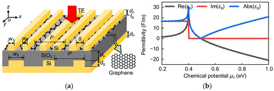
Figure 1.
(a) Schematic of the near-perfect proposed graphene absorber. (b) Relationship between permittivity and chemical potential of graphene at 1550 nm.
Monolayer graphene was modeled as an ultrathin dielectric layer with a thickness of tg = 0.34 nm. The material properties of graphene can be described by its surface conductivity, which can be obtained using the Kubo equation [38,39]:
where σintra(ω) and σinter(ω) represent the intra- and inter-band transition conductivities, ω is the angular frequency, e is the charge of an electron, is the reduced Planck constant, and kB is the Boltzmann constant. T = 300 K is the Kelvin temperature, Γ = 1/2τ is related to the electron–phonon relaxation time τ, chemical potential of graphene µc = 0.3 eV, Fermi velocity υF = 106 m/s, and carrier mobility μ = 104 cm2/(V·s) [40]. The relationship between the surface conductivity σgra and the relative permittivity of monolayer graphene can be expressed by the following formula: εgra = 1 + iσgra/ωε0tg, where ε0 is the vacuum permittivity [41]. Figure 1b shows the relationship between the chemical potential and permittivity of the monolayer graphene at 1550 nm. The permittivity of graphene strongly depends on its chemical potential, and the imaginary part of the permittivity decreases sharply when the chemical potential is approximately 0.4 eV.
The proposed resonant system based on a dual-layer asymmetric meta-grating structure can be considered a single-port lossless resonator. According to coupled-mode theory (CMT), the absorption efficiency of the proposed device can be calculated as follows [27,42]:
where γ and δ represent the external leakage rates and inherent losses of materials in the proposed structure, respectively, and ω and ω0 represent the working frequency and the central resonant frequency, respectively. When the intrinsic loss of the material is equal to the external leakage rate, that is δ = γ, the system reaches the critical coupling condition, and the total absorption of monolayer graphene can be realized at the resonant frequency ω0.
3. Results and Discussion
Theoretically, maintaining δ = γ of the resonance is critical for achieving critical coupling, and the intrinsic loss δ is almost constant. Therefore, controlling the external leakage rate γ plays a key role in achieving critical coupling. We first demonstrate the relationship between various structural parameters and the external leakage rate, and the influence of the structural parameters on the absorption of the proposed structure. Figure 2a shows the calculated absorption as a function of the wavelength for the proposed structure as the gap g increases from 0 to 84 nm. The efficiency of the absorption peak first increases gradually, owing to the enhanced excitation intensity of the resonant mode. For g = 21 nm, the maximum light absorption of the monolayer graphene reached 99.6%. As g further increased, the absorption efficiency became relatively weak, and the bandwidth of the absorption peak gradually increased. To better explain the effect of the spacing g on the entire resonant system, the phase diagrams at different g values were calculated, as shown in Figure 2b. The sharp π-phase transition at g = 21 nm indicates that a critical coupling condition is achieved [43,44]. A nearly perfect absorption peak with a bandwidth of 0.4 nm is achieved at 1550.6 nm, as shown in Figure 2c. We then compared the theoretical results from the CMT with the simulation results from the rigorous coupled-wave analysis (RCWA) and finite element method (FEM) methods. The total quality factory of the entire structure can be expressed as QCMT = QδQγ/(Qδ + Qγ), where Qδ = ω0/2δ and Qγ = ω0/2γ represent the intrinsic loss and external leakage, respectively. The fitted δ = γ = 1.2477 × 10¹⁰ Hz was obtained when critical coupling occurred, and the value of QCMT was 3876.5328.
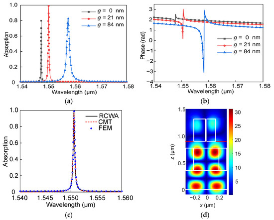
Figure 2.
(a) Absorption spectra under different grating gaps g. (b) Phase change diagrams corresponding to different g. (c) Comparison of the absorption spectrum obtained from the theoretical calculation and numerical simulation results. (d) Electric field distribution at the resonant wavelength of 1550.6 nm.
By contrast, the total quality factor Q can be acquired from Q = λ0/FWHM, where the full width at half maximum (FWHM) is only 0.4 nm at the resonant wavelength of 1550.6 nm. Thus, we obtained Q = 3876.5. The value of QCMT and Q are almost the same, indicating that the theoretical results agree with the simulation results. To better explore the physical mechanism of the narrow-band absorption peaks, Figure 2d shows the electric field amplitude distribution of the designed structure on the x-z plane at a resonant wavelength of 1550.6 nm. One can see that most of the electric field is concentrated on the bottom grating of the designed structure. In other words, the strong localization ability of ZCG in the designed structure significantly enhances the interaction between light and graphene.
Furthermore, we studied the dependence of the absorption spectrum on the spacer layer thickness in the designed structure, as shown in Figure 3. The absorption map of the proposed system for different spacer layers ds is shown in Figure 3a. The results show that the absorption peak blue-shifts with increasing spacer thickness when the thickness of the spacer layer is less than 100 nm. A near-perfect absorption spectrum is achieved at the wavelength of 1550.6 nm when ds = 128 nm. However, the position of the absorption peak keeps unchanged when ds is greater than 150 nm. To further investigate this phenomenon. We calculate the reflection spectra of the designed structure under different ds, as shown in Figure 3b. One can see that the reflection spectrum at the wavelength of 1550.6 nm gradually disappears when ds gradually increased from 0 to 250 nm. Here, an accidental BICs’ state that can occur in any structure but requires careful adjustment of the parameters is excited [45]. In addition, the bandwidth of the absorption peak decreases rapidly as ds increases from 0 to 300 nm. The FEM can rigorously calculate the eigenvalues of the structure, and the complex eigenvalues N can be described with the formula N = Nreal − iNimag [46]. To further explain the regulation mechanism of spacer layer thickness on the absorption spectra, we use the FEM to calculate the complex eigenvalue N of the proposed structure without graphene at different ds, as shown in Table 1. The imaginary part of the complex eigenvalue decreases with an increase in ds, and the real part increases gradually and then remains unchanged. As a result, the complex eigenvalue plays a key role in determining the absorption performance in the designed graphene absorbers with difficult ds.
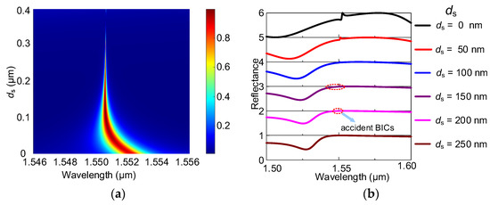
Figure 3.
(a) Absorption maps of the proposed structure for the different thicknesses of spacer layer ds. (b) Reflection spectra under different ds.

Table 1.
Complex eigenvalues N corresponding to different thicknesses of the spacer layer.
Subsequently, we studied the influence of waveguide thickness dh and grating period P on the absorption spectra. According to Figure 4a, the central resonant wavelength exhibits a red-shifts as dh varies from 335 to 375 nm. The absorption efficiency of the proposed dual-layer asymmetric meta-grating structure is high, which differs from our previous work [29]. Figure 4b shows the absorption spectra of the designed structure when the period P increases from 666 to 726 nm. The results show that the absorption wavelength shifts to the long-wave direction as the period increases because the successful excitation of guided-mode resonance must satisfy the phase-matching condition [47]. Meanwhile, the absorption spectrum maintained a high absorption efficiency when the period varied in the range of 60 nm. The results in Figure 4 show that the spectral position of the absorption peak can be controlled by tailoring the grating waveguide layer thickness or grating period. The realization of adjustable and switchable functions that satisfy the requirements of actual equipment has become the main direction of current research [48]. In our proposed graphene absorber with a dual-layer asymmetric meta-grating structure, the resonant wavelength can be adjusted by adjusting the thickness of the waveguide layer or grating period, which meets the requirement of wavelength tunability.
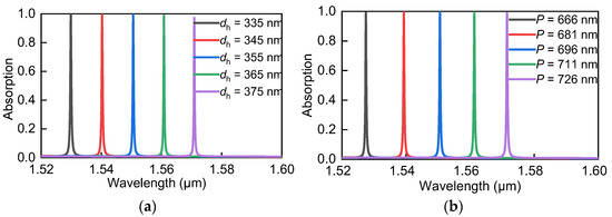
Figure 4.
(a) Absorption spectra of the proposed structure with different waveguide layer thicknesses dh. (b) Absorption spectra of the proposed structure with different grating periods P.
In the above analysis, we adjusted the absorption efficiency and the spectral position of the absorption peak by changing the structural parameters. However, it is undesirable to change the size of the absorber or further adjust the wavelength of the absorption peak by refabricating a new structure for practical applications. The chemical potential of graphene can be controlled by external gate voltage [49]. The relative permittivity of graphene changes with the chemical potential as shown in Figure 1b. Therefore, the influence of the chemical potential μc of monolayer graphene on the absorption response of the structure was studied based on the tunable properties of graphene [50]. Figure 5a shows that the absorption efficiency of the absorption peak can be flexibly tuned by changing the chemical potential. The absorption efficiency and resonant wavelength change simultaneously when the structural parameter g is changed. Here, a dynamic adjustment of the graphene absorption efficiency is realized at a specific wavelength by controlling the chemical potential μc. Figure 5b shows the absorption of graphene as a function of μc at a wavelength of 1550.6 nm. When μc increases from 0.2 to 0.34 eV, the absorption of graphene remains unchanged, and the corresponding modulation depth is minimal [50]. When uc changes from 0.34 to 0.51 eV, the absorption efficiency of graphene can be flexibly regulated, and the position of the absorption peak remains unchanged. As μc increases from 0.51 to 0.8 eV, the absorption efficiency of graphene is finally modulated to very close to zero. Moreover, according to reference [37], the absorption of graphene can exhibit the characteristics of electrical switches when μc changes from 0.34 to 0.51 eV. Among them, high absorption efficiency is marked as an “on” state, and low absorption efficiency is marked as an “off” state. Unlike the wired control method, we can control the driving signal in a noncontact manner by adjusting the optical signal with the designed dual-layer asymmetric meta-grating structure, which shows great potential in integrated optical systems [51].
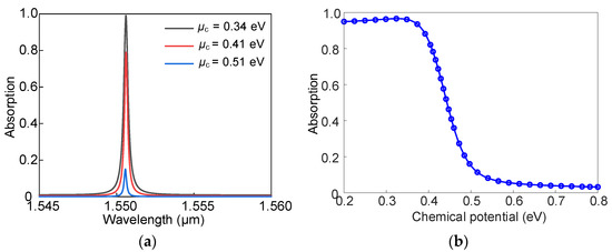
Figure 5.
(a) Absorption spectra of designed structures under different chemical potentials μc. (b) Effect of chemical potential μc on the absorption efficiency at 1550.6 nm.
4. Conclusions
In this study, using a dual-layer asymmetric meta-grating structure, we obtained a narrow-band tunable graphene absorber in the communication band. The calculation results show that the absorption ability of monolayer graphene is dramatic owing to the strong localization ability of the ZCG at the bottom of the structure to the light field. By adjusting the structural parameters of the grating, the designed graphene-based absorber exhibited excellent wavelength tunability. Interestingly, accidental BICs can be realized while adjusting the linewidth by changing the thickness of the spacer layer. Moreover, based on the tunable properties of graphene, the proposed structure achieved a dynamically tunable absorption efficiency at a specific wavelength after changing the chemical potential of graphene. This research has great potential for application in high-performance optical detection, modulation, sensing, and advanced integrated optical systems.
Author Contributions
Conceptualization, J.H.; funding acquisition, J.H.; methodology, J.L. and J.H.; project administration, J.H. and J.Z.; software, J.L. and X.L.; supervision, J.H. and J.Z.; writing–original draft, J.L.; writing–review and editing, J.H., X.L. and J.Z. All authors have read and agreed to the published version of the manuscript.
Funding
This research was funded by the National Natural Science Foundation of China (Grant No. 61905060), the Scientific Research Project of the Department of Education of Hebei Province, China (Grant No. ZD2021019), and the Open Project of the Shandong Key Laboratory of Optics and Photonic Device, China (Grant No. K202104).
Institutional Review Board Statement
Not applicable.
Data Availability Statement
Not applicable.
Acknowledgments
This manuscript has not yet been published and is not under consideration for publication elsewhere. The authors are grateful to those who participated in the study.
Conflicts of Interest
The authors declare no conflict of interest.
References
- Duplock, E.J.; Scheffler, M.; Lindan, P.J.D. Hallmark of perfect graphene. Phys. Rev. Lett. 2004, 92, 225502. [Google Scholar] [CrossRef] [PubMed]
- Sarma, S.D.; Adam, S.; Hwang, E.H.; Rossi, E. Electronic transport in two-dimensional graphene. Rev. Mod. Phys. 2011, 83, 407. [Google Scholar] [CrossRef]
- Qing, Y.M.; Ren, Y.Z.; Lei, D.Y.; Ma, H.F.; Cui, T.J. Strong coupling in two-dimensional materials-based nanostructures: A review. J. Opt. 2022, 24, 024009. [Google Scholar] [CrossRef]
- Luo, X.; Zhou, Y.G.; Cai, Y.J.; Cheng, Z.Q.; Liu, Z.M.; Wang, W.Q. A review of perfect absorbers based on the two dimensional materials in the visible and near-infrared regimes. J. Phys. D Appl. Phys. 2021, 55, 093002. [Google Scholar] [CrossRef]
- Furchi, M.; Urich, A.; Pospischil, A.; Lilley, G.; Unterrainer, K.; Detz, H.; Klang, P.; Andrews, A.M.; Schrenk, W.; Strasser, G.; et al. Microcavity-integrated graphene photodetector. Nano Lett. 2012, 12, 2773–2777. [Google Scholar] [CrossRef] [PubMed]
- Liu, C.H.; Chang, Y.C.; Norris, T.B.; Zhong, Z.H. Graphene photodetectors with ultra-broadband and high responsivity at room temperature. Nat. Nanotechnol. 2014, 9, 273–278. [Google Scholar] [CrossRef]
- Zhang, J.F.; Zhu, Z.H.; Liu, W.; Yuan, X.D.; Qin, S.Q. Towards photodetection with high efficiency and tunable spectral selectivity: Graphene plasmonics for light trapping and absorption engineering. Nanoscale 2015, 32, 13530–13536. [Google Scholar] [CrossRef]
- Guan, H.Y.; Hong, J.Y.; Wang, X.L.; Ming, J.Y.; Zhang, Z.L.; Liang, A.J.; Han, X.Y.; Dong, J.L.; Qiu, W.T.; Chen, Z.; et al. Broadband, high-sensitivity graphene photodetector based on ferroelectric polarization of lithium niobate. Adv. Opt. Mater. 2021, 9, 2100245. [Google Scholar] [CrossRef]
- Ojaghi, S.; Golmohammadi, S.; Soofi, H. All-optical hybrid plasmonic waveguide modulator based on Kerr nonlinearity of graphene. Opt. Eng. 2022, 61, 117102. [Google Scholar] [CrossRef]
- Zhong, C.Y.; Li, J.Y.; Lin, H.T. Graphene-based all-optical modulators. Front. Optoelectron. 2020, 13, 114–128. [Google Scholar] [CrossRef]
- Rahim, A.; Hermans, A.; Wohlfeil, B.; Petousi, D.; Kuyken, B.; Van Thourhout, D.; Baets, R.G. Taking silicon photonics modulators to a higher performance level: State-of-the-art and a review of new technologies. Adv. Photonics 2021, 3, 024003. [Google Scholar] [CrossRef]
- Liu, S.Y.; Wang, M.Z.; Liu, T.Y.; Xu, Y.; Yue, J.B.; Sun, X.Q.; Zhang, D.M. Polarization-insensitive graphene modulator based on hybrid plasmonic waveguide. Photonics 2022, 9, 609. [Google Scholar] [CrossRef]
- Jin, M.; Wei, Z.Y.; Meng, Y.F.; Shu, H.W.; Bai, B.W.; Wang, X.J. Silicon-based graphene electro-optical modulators. Photonics 2022, 9, 82. [Google Scholar] [CrossRef]
- Shi, B.; Cai, W.; Zhang, X.Z.; Xiang, Y.X.; Zhan, Y.; Geng, J.; Ren, M.X.; Xu, J.J. Tunable band-stop filters for graphene plasmons based on periodically modulated graphene. Sci. Rep. 2016, 6, 26796. [Google Scholar] [CrossRef]
- Zhu, Z.H.; Guo, C.C.; Liu, K.; Zhang, J.F.; Ye, W.M.; Yuan, X.D.; Qin, S.Q. Electrically controlling the polarizing direction of a graphene polarizer. J. Appl. Phys. 2014, 116, 104304. [Google Scholar] [CrossRef]
- Maleki, M.; Mehran, M. Analytical investigation and systematic design approach for high-sensitivity guided mode resonance sensors with graphene-enabled tunability. IEEE Sens. J. 2022, 22, 14177–14184. [Google Scholar] [CrossRef]
- Mousavi-Kiasari, S.M.G.; Rashidi, K.; Fathi, D.; Taleb, H.; Mirjalili, S.M.; Faramarzi, V. Computational design of highly-sensitive graphene-based multilayer SPR biosensor. Photonics 2022, 9, 688. [Google Scholar] [CrossRef]
- Nair, R.R.; Blake, P.; Grigorenko, A.N.; Novoselov, K.S.; Booth, T.J.; Stauber, T.; Peres, N.M.R.; Geim, A.K. Fine structure constant defines visual transparency of graphene. Science 2008, 320, 1308. [Google Scholar] [CrossRef]
- Mak, K.F.; Sfeir, M.Y.; Wu, Y.; Lui, C.H.; Misewich, J.A.; Heinz, T.F. Measurement of the optical conductivity of graphene. Phys. Rev. Lett. 2008, 101, 196405. [Google Scholar] [CrossRef]
- Zhou, K.; Cheng, Q.; Song, J.; Lu, L.; Luo, Z.X. Highly efficient narrow-band absorption of a graphene-based Fabry–Perot structure at telecommunication wavelengths. Opt. Lett. 2019, 44, 3430–3433. [Google Scholar] [CrossRef]
- Zhao, B.; Zhao, J.M.; Zhang, Z.M. Enhancement of near-infrared absorption in graphene with metal gratings. Appl. Phys. Lett. 2014, 105, 031905. [Google Scholar] [CrossRef]
- Wu, J. Enhancement of absorption in graphene strips with cascaded grating structures. IEEE Photonics Technol. Lett. 2016, 28, 1041–1135. [Google Scholar] [CrossRef]
- Zhang, H.J.; Zheng, G.G.; Xian, F.L.; Zou, X.J.; Wang, J.C. Near-unity absorption of graphene monolayer with a triple-layer waveguide coupled grating. Opt. Mater. 2017, 72, 476–481. [Google Scholar] [CrossRef]
- Hu, J.H.; Fu, J.; Liu, X.H.; Ren, D.P.; Zhao, J.J.; Huang, Y.H. Perfect absorption in a monolayer graphene at the near-infrared using a compound waveguide grating by robust critical coupling. Chin. Opt. Lett. 2019, 17, 010501. [Google Scholar]
- Hu, J.H.; Huang, Y.Q.; Duan, X.F.; Wang, Q.; Zhang, X.; Wang, J.; Ren, X.M. Enhanced absorption of graphene strips with a multilayer subwavelength grating structure. Appl. Phys. Lett. 2014, 105, 221113. [Google Scholar] [CrossRef]
- Zhang, X.W.; John, S. Broadband light-trapping enhancement of graphene absorptivity. Phys. Rev. B Condens. Matter 2019, 99, 035417. [Google Scholar] [CrossRef]
- Piper, J.R.; Fan, S.H. Total absorption in a graphene monolayer in the optical regime by critical coupling with a photonic crystal guided resonance. ACS Photonics 2014, 1, 345–353. [Google Scholar] [CrossRef]
- Wang, X.; Duan, J.Y.; Chen, W.Y.; Zhou, C.B.; Liu, T.T.; Xiao, S.Y. Controlling light absorption of graphene at critical coupling through magnetic dipole quasi-bound states in the continuum resonance. Phys. Rev. B 2020, 102, 155432. [Google Scholar] [CrossRef]
- Hu, J.H.; Liang, J.F.; Zou, J.; Shi, C.Y.; Zhao, J.J. Dual-band perfect graphene absorber with an all-dielectric zero-contrast grating-based resonant cavity. Opt. Commun. 2023, 527, 128908. [Google Scholar] [CrossRef]
- Jiang, L.Y.; Yuan, C.; Li, Z.Y.; Su, J.; Yi, Z.; Yao, W.T.; Wu, P.H.; Liu, Z.M.; Cheng, S.B.; Pan, M. Multi-band and high-sensitivity perfect absorber based on monolayer graphene metamaterial. Diam. Relat. Mater. 2021, 111, 108227. [Google Scholar] [CrossRef]
- Qing, Y.M.; Ma, H.F.; Cui, T.J. Flexible control of light trapping and localization in a hybrid Tamm plasmonic system. Opt. Lett. 2019, 44, 3302–3305. [Google Scholar] [CrossRef] [PubMed]
- Heo, H.; Lee, S.; Kim, S. Broadband absorption enhancement of monolayer graphene by prism coupling in the visible range. Carbon 2019, 154, 42–47. [Google Scholar] [CrossRef]
- Chen, J.; Zhang, M.X.; Gu, P.; Yan, Z.D.; Tang, C.J.; Lv, B.; Wang, X.X.; Yi, Z.; Zhu, M.W. Broadband, wide-incident-angle, and polarization-insensitive high-efficiency absorption of monolayer graphene with nearly 100% modulation depth at communication wavelength. Results Phys. 2022, 40, 105833. [Google Scholar] [CrossRef]
- Wu, F.; Liu, D.J.; Xiao, S.Y. Bandwidth-tunable near-infrared perfect absorption of graphene in a compound grating waveguide structure supporting quasi-bound states in the continuum. Opt. Express 2021, 29, 41975–41989. [Google Scholar] [CrossRef]
- Xiao, S.Y.; Liu, T.T.; Wang, X.; Liu, X.J.; Zhou, C.B. Tailoring the absorption bandwidth of graphene at critical coupling. Phys. Rev. B 2020, 102, 085410. [Google Scholar] [CrossRef]
- Zhang, S.S.; Liu, H.X.; Zhang, J.; Li, W.J.; Wang, H.; Tian, C.X.; Luo, L.; Zhao, L.J. Dynamically switchable triple-band absorption enhancement of graphene by a subwavelength grating coupled hybrid structure. Results Phys. 2022, 43, 106057. [Google Scholar] [CrossRef]
- Qing, Y.M.; Ma, H.F.; Ren, Y.Z.; Cui, T.J. Near-infrared absorption-induced switching effect via guided mode resonances in a graphene-based metamaterial. Opt. Express 2019, 27, 5253–5263. [Google Scholar] [CrossRef]
- Hanson, G.W. Dyadic Green’s functions and guided surface waves for a surface conductivity model of graphene. J. Appl. Phys. 2008, 103, 064302. [Google Scholar] [CrossRef]
- Lu, H.; Gan, X.T.; Mao, D.; Zhao, J.L. Graphene-supported manipulation of surface plasmon polaritons in metallic nanowaveguides. Photonics Res. 2017, 5, 162–167. [Google Scholar] [CrossRef]
- Thongrattanasiri, S.; Koppens, F.H.L.; De Abajo, F.J.G. Complete optical absorption in periodically patterned graphene. Phys. Rev. Lett. 2012, 108, 047401. [Google Scholar] [CrossRef]
- Bian, L.A.; Yang, L.; Liu, P.G.; Chen, Y.W.; Liu, H.Q.; Zhou, Q.H. Controllable perfect absorption in a double-cavity photonic crystal with one graphene monolayer. J. Phys. D Appl. Phys. 2017, 51, 025106. [Google Scholar] [CrossRef]
- Fan, S.H.; Suh, W.; Joannopoulos, J.D. Temporal coupled-mode theory for the Fano resonance in optical resonators. J. Opt. Soc. Am. A 2003, 20, 569–572. [Google Scholar] [CrossRef] [PubMed]
- Yoon, J.; Seol, K.H.; Song, S.H.; Magnusson, R. Critical coupling in dissipative surface-plasmon resonators with multiple ports. Opt. Express 2010, 18, 25702–25711. [Google Scholar] [CrossRef] [PubMed]
- Qing, Y.M.; Ma, H.F.; Cui, T.J. Tailoring anisotropic perfect absorption in monolayer black phosphorus by critical coupling at terahertz frequencies. Opt. Express 2018, 26, 32442–32450. [Google Scholar] [CrossRef] [PubMed]
- Vyas, H.; Hegde, R.S. Improved refractive-index sensing performance in medium contrast gratings by asymmetry engineering. Opt. Mater. Express 2020, 10, 1616–1629. [Google Scholar] [CrossRef]
- Huang, L.J.; Xu, L.; Rahmani, M.; Neshev, D.; Miroshnichenko, A.E. Pushing the limit of high-Q mode of a single dielectric nanocavity. Adv. Photonics 2021, 3, 016004. [Google Scholar] [CrossRef]
- Wang, S.S.; Magnusson, R. Theory and applications of guided-mode resonance filters. Appl. Opt. 1993, 32, 2606–2613. [Google Scholar] [CrossRef]
- Xiao, S.Y.; Qin, M.B.; Duan, J.Y.; Wu, F.; Liu, T.T. Polarization-controlled dynamically switchable high-harmonic generation from all-dielectric metasurfaces governed by dual bound states in the continuum. Phys. Rev. B 2022, 105, 195440. [Google Scholar] [CrossRef]
- Vakil, A.; Engheta, N. Transformation optics using graphene. Science 2011, 332, 1291–1294. [Google Scholar] [CrossRef]
- Yan, Z.D.; Kong, L.C.; Tang, C.J.; Deng, J.; Gu, P.; Chen, J.; Wang, X.X.; Yi, Z.; Zhu, M.W. Ultra-broadband and completely modulated absorption enhancement of monolayer graphene in a near-infrared region. Opt. Express 2022, 30, 34787–34796. [Google Scholar] [CrossRef]
- Zhang, X.G.; Sun, Y.L.; Zhu, B.C.; Jiang, W.X.; Zhang, Z.C.; Cui, T.J. Light-controllable time-domain digital coding metasurfaces. Adv. Photonics 2022, 4, 025001. [Google Scholar] [CrossRef]
Disclaimer/Publisher’s Note: The statements, opinions and data contained in all publications are solely those of the individual author(s) and contributor(s) and not of MDPI and/or the editor(s). MDPI and/or the editor(s) disclaim responsibility for any injury to people or property resulting from any ideas, methods, instructions or products referred to in the content. |
© 2022 by the authors. Licensee MDPI, Basel, Switzerland. This article is an open access article distributed under the terms and conditions of the Creative Commons Attribution (CC BY) license (https://creativecommons.org/licenses/by/4.0/).