Article

Design and Validation of a Reduced Switching Components Step-Up Multilevel Inverter (RSCS-MLI)

1
Department of Electric Power Engineering, Budapest University of Technology and Economics, 1111 Budapest, Hungary
2
Department of Electrical Engineering, ZHCET, Aligarh Muslim University, Aligarh 202002, India
3
Industrial Engineering Department, College of Engineering, King Saud University, P.O. Box 800, Riyadh 11421, Saudi Arabia
4
School of Electrical and Data Engineering, University of Technology Sydney, Sydney 2000, Australia
*
Authors to whom correspondence should be addressed.
Processes 2021, 9(11), 1948; https://doi.org/10.3390/pr9111948
Submission received: 21 July 2021 / Revised: 18 October 2021 / Accepted: 25 October 2021 / Published: 29 October 2021
(This article belongs to the Section Energy Systems)

Abstract

:
A reduced switching components step-up multilevel inverter (RSCS-MLI) is presented in the paper. The basic circuit of the proposed MLI can produce 11 levels in the output voltage with a reduced number of switching components. The other features of the proposed circuit include a low value of voltage stresses and the inherent generation of the voltage levels pertaining to the negative half without the requirement of an H-bridge. Fundamental frequency switching technique, also known as Nearest Level Control (NLC) technique, is implemented in the proposed topology for generating the switching signals. The experimental total harmonic distortion (THD) in the output voltage comes out to be 9.4% for modulation index equal to 1. Based on different parameters, a comparative study has been shown in the paper, which makes the claim of the proposed MLI stronger. An experimental setup is prepared to carry out the hardware implementation of the proposed structure and monitor its performance under dynamic load conditions, which is also used to verify the simulation results. Power loss analysis, carried out by using PLECS software, helps us to gain insight into different losses occurring while operating the inverter. The different results are explained and analyzed in the paper.

1. Introduction

Multilevel inverters are the main components in low to high voltage industrial applications such as electric vehicles, HVDC, FACTS devices, renewable power generation plants, micro grids etc. MLIs have low dv/dt characteristics, superior efficiency, better EMC, modularity, and fault tolerance capabilities, making it more advantageous than the two-level inverter [1,2,3]. Conventionally, there are three categories of the MLIs as cascaded H-bridge (CHB), neutral point clamped (NPC), and flying capacitor (FC) MLIs [4,5,6]. These topologies have drawbacks such as a high number of dc sources, switches, and other components. Additionally, they suffer from high voltage stress, high harmonic distortions etc. The research performed in the development of MLIs helped in reducing the components of the MLIs, which is essential and recommended. Many of the combinations of the components introduce different topologies of the MLIs. One of the topologies is packed U-cell topologies which have the advantage of the FCMLI but comes with high switching stress [7]. Additionally, capacitor voltage balancing is complex and requires space vector modulation or selective harmonic elimination technique. A reduced component extended topology is presented in [8] with three dc voltage sources. With the increase in level, the number of the dc source increase. Another 11-level multilevel inverter topology is proposed with fewer components and three dc voltage sources [9]. A MLI topology with voltage boosting capabilities comprises an input inductor, a boost converter with a voltage multiplier circuit is presented in [10]. In [11], various PWM methods are analyzed with a three-phase 11-level inverter and a reduced number of switches.
A topology [12] having reduced power switches to achieve the analogous results of existing CHB configuration with the help of carrier-based sinusoidal technique. The authors discuss a seventeen-level topology focus on the inverter’s boosted operation with fewer switches in [13]. The proposed structure utilizes 10 switches along with two dc sources and three capacitors. A PV array input-based eleven-level MLI is proposed in [14] with high output current quality and very low THD value. A multilevel inverter topology with n level is presented in [15]. The topology can be used in high voltage application. A modified switched capacitor is discussed in [16]. The presented topology produces 13 levels with nine switches and three dc voltage sources. Another multilevel inverter with a boosting feature comprising a switched capacitor with 7 achievable voltage levels has been introduced [17]. In [18], a single phase eleven-level inverter based on switched-capacitor is presented. The presented topology has self-balance capability and reduce components. Modulation techniques are vital in determining the total harmonic distortion in an MLI structure. Various modulation/switching techniques are nearest level control (NLC), selective harmonic elimination (SHE) based methods, space vector modulation (SVM) etc. A modified nearest level control method is discussed in [19] which has been implemented on cascaded h-bridge inverters with the aim to reduce THD. A novel configuration of MLI is presented in [20], which is called the K-type module. It requires 14 semiconductor switches, two dc sources, and two capacitors to obtain the 13-level output. Some more recent Switched-Capacitor-based topologies are discussed in [21,22,23,24,25].
The article is presented as follows: Section 1 explains the literature survey which contains work done by researchers previously. Section 2 presents the details of the design and working of the proposed converter. NLC Modulation strategy is explained in Section 3. Power loss analysis, which consists of mathematical expressions and various graphs, is deliberated in Section 4. The comparison with other topologies is presented in Section 5. The simulation results and the hardware implementation of the proposed topology is presented in Section 6. The different results are shown and explained. The article concludes with Section 7.

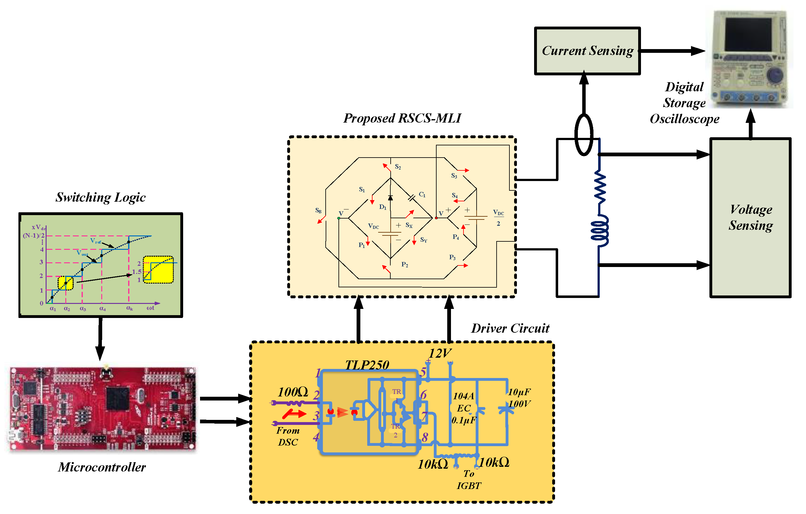
2. Proposed RSCS-MLI Circuit

2.1. Description and Operation

The proposed inverter (Figure 1) involves two dc sources, one capacitor besides 11 semiconductor power switches i.e., S1, S2, S3, S4, P1, P2, P3, P4, SX, SY and SB. The ratio of magnitudes of the dc sources used here is 2:1 i.e., the magnitudes of dc sources are VDC and VDC/2. The 11-levels can be generated by the circuit in which five are positive (+0.5 VDC, +VDC, +1.5 VDC, +2 VDC and +2.5 VDC), five are negative levels (−0.5 VDC, −VDC, −1.5 VDC, −2 VDC and −2.5 VDC) and a zero voltage level i.e., Vo = 0. The stress on the switches Sx, S1, S2, P1, P2 and SB is equal to the input voltage whereas the switches S3, P3, P4 and S4 have blocking voltage of 0.5 VDC. The floating capacitor’s voltage is maintained at VDC.
The switching states pertaining to all the voltage levels are placed in Table 1. The conduction levels are discussed below:
Zero level (0 V): The zero states can be achieved either by turning on the switches S1, S2, S3, S4 or P1, P2, P3, P4. The capacitor starts charging with the path VDC, D1, C1, SY during the zero level and settles at the voltage VDC. There is no necessity of an h-bridge to change the polarity as it is an inherent feature of the topology.
First level (+VDC/2): The first level follows the path as P1, SY, C1, S2, S3, −VDC/2, and P4. This result in formation of first level with voltage level 0.5 VDC. The capacitor’s voltage remains settled at VDC.
Second level (+VDC): For the second level with voltage magnitude of VDC, the switches which remain in conduction are P1, SY, C1, S2, S3, and S4. In this mode, no changes are observed in the capacitor voltage.
Third level (+3 VDC/2): In this level, the output is produced by the additive nature of the VDC, capacitor C1, and the −VDC/2. The conduction path is P1, VDC, SX, C1, S2, S3, −VDC/2, and P4. The capacitor starts discharging in this mode. The output of this level is 1.5VDC.
Fourth level (+2 VDC): This level is obtained by following the path as P1, VDC, SX, C1, S2, S3, and S4. The output of this level is 2 VDC which is achieved with the help of capacitor C1.
Fifth level (+5 VDC/2): In this level the switch SB, conducts for the first time, helping in producing the fifth level whose output is 2.5 VDC. The conduction path is as P1, VDC, SX, C1, S2, SB, P3, +VDC/2, and S4. Similarly, the negative levels are achieved as according to those given in the Table 1. Figure 2 shows the conduction diagram for the various output voltage levels.

2.2. Total Standing Voltage

The voltage stress or the voltage required to be blocked by the switches governs the rating of power switches to be used in the implementation of the MLI circuit. Total Standing Voltage (TSV) refers to the total sum of the voltage stresses on all the switches in the circuit. Therefore, a low value of TSV indicates that the low rating switches can be used, which means the cost of the switches is lower, ultimately deciding the overall cost of the inverter circuit. Additionally, if TSV is lower the stress on the switches is low hence the life of the switches increase. In the present topology, the magnitude of DC voltage sources are in the ratio of 2:1. The blocking voltage on different switches are shown in Figure 3.
Mathematically, the TSV for the proposed MLI topology is calculated as given below:
TSV = VS1 + VS2 + VS3 + VS4 + VP1 + VP2 + VP3 + VP4 + VSB + VSx + VSy + VSb = (2 + 2 + 0.5+ 0.5 + 2 + 2 + 0.5 + 0.5 + 1 + 1 + 0.5 + 0.5) VDC = 12.5 VDC
The TSV magnitude can be divided by the maximum output voltage to obtain the per-unit TSV. For the proposed topology here, it is calculated as follows:
P e r U n i t   T S V ( T S V p . u . ) =   T S V M a x i m u m   O u t p u t   V o l t a g e = 12.5 2.5 = 5

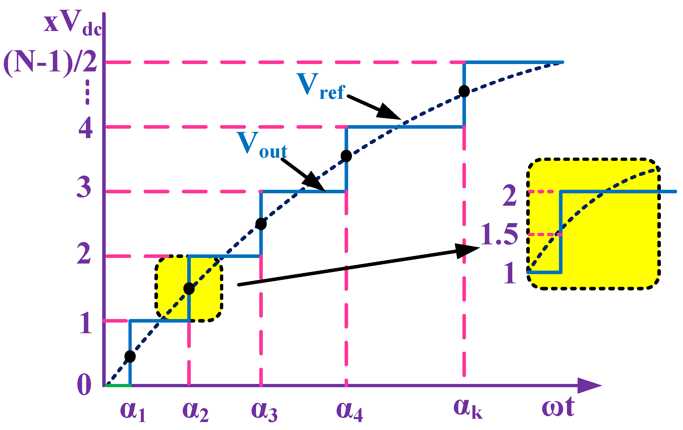
3. Modulation Technique

Various pulse width modulation (PWM) techniques can be used to generate the signals required for giving pulses to different switches. They are broadly categorized into high (sinusoidal PWM, level-shifted and phase shifted PWM etc.) and low frequency (NLC-PWM, SHE-PWM, SVM-PWM etc.) modulation techniques. The advantage with the low frequency switching techniques is the low value of losses in the switches as there is less transition in the ON and OFF state of the switches [16]. In the proposed work, NLC modulation technique has been in the proposed MLI. To generate switching pulses, a sine wave is taken as a reference. The NLC switching scheme is shown in Figure 4. The Firing angle is calculated [17] as:
α i = sin 1 ( i 0.5 n ) ;   f o r   i = 1 , 2 , 3 n = N 1 2

4. Power Loss Analysis

In operating the power circuit, various losses occur in the power switches. These losses are due to switching transitions as well as due to their conduction. The losses pertaining to the transition of switches i.e., turning the switches ON and OFF, are termed as switching losses. On the other hand, conduction losses are due to the conduction of the switches. To calculate these losses, the power loss analysis of the circuit should be taken into consideration. Therefore, the thermal modelling of the proposed converter has been done in PLECS software, and different losses have been recorded. The loss can be calculated with the sum of conduction losses and switching losses. The thermal loss profile for the IGBT FGA25N120 is shown in Figure 5. The thermal description depicting the turn-on loss, turn-off loss, and conduction loss have been shown in Figure 5a–c, respectively. This is completed in a PLECS environment with the help of heat sink and the thermal resistance of 1K/W at the ambient temperature of 25 °C. The plot shows the two temperatures as 25 °C and 150 °C which cover loss model based on manufacturers data. The operating junction temperature and storage temperature ranges from −55 to +150 °C. These losses are described as follows:

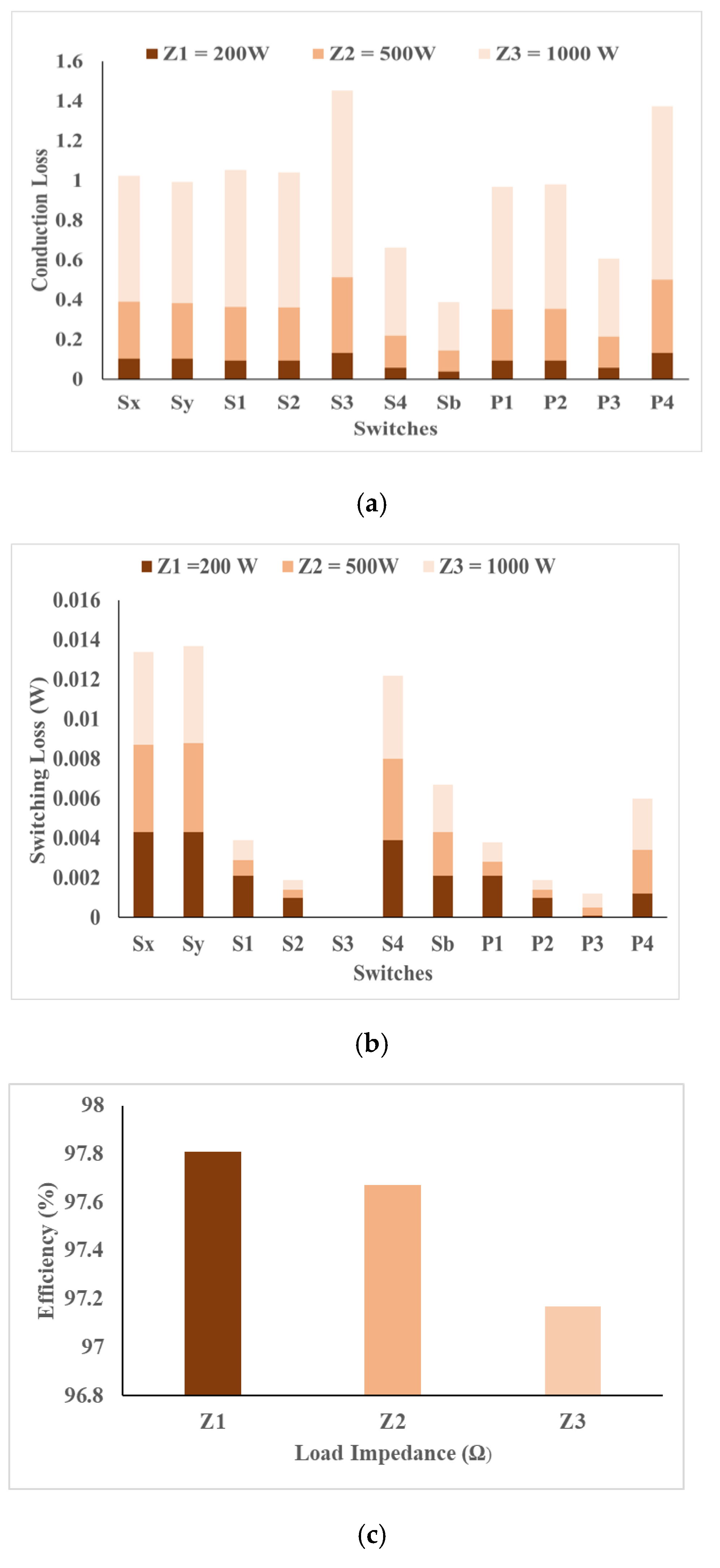
4.1. Conduction Losses

When the switches i.e., IGBT, ON due to the internal resistance the current experience an oppose to flow which cause losses in the switches. This loss in the switch is called conduction loss. Mathematically the conduction loss can be expressed as:
P C o n d L o s s = A l l   S w i t c h e s I O N 2 × R I n t e r n a l
where ION is the current flowing through the switches during conduction, RInternal is the internal resistance of the switch.

4.2. Switching Losses

The power dissipated in the switch during turning ON and OFF is known as switching losses. The switching loss includes the turn-ON losses and the turn-OFF losses which can be calculated as elaborated in [26].
E O F F , n = 0 t O F F v ( t ) i ( t ) d t E O F F , n = 0 t O F F ( V s w , n t O F F t ) ( I t O F F ( t t O F F ) ) d t E O F F , n = V O F F , n × I O F F , n   6
Similarly, one can calculate the energy loss occurred during turning ON the switch which can be expressed as:
E O N , n = V O N , n × I O N , n   6
where EOFF,n and EON,n—turn off and turn on energy loss for the n switch at time tOFF and tON, respectively. Mathematically, the power loss occurs when the switch changes its state from OFF to ON is give as:
P S W L O S S = n 1 f O U T P U T V O N , n × I O N , n × T O N , n 6 + V O F F , n × I O F F , n × T O F F , n 6
where VON, ION, TON and VOFF, IOFF, TOFF are the respective parameters for the ON and OFF state of the switch. fOUTPUT is output voltage frequency.
Finally, the total loss can be calculated as the sum of conduction loss and switching loss. Therefore,
P T L o s s = P C o n d L O S S + P S W L O S S
The simulation results are developed in the environment of PLECS. Three different loading conditions such as Z1 = 200 W (400 Ω), Z2 = 500 W (150 Ω + 70 mH), and Z3 = 1 kW (60 + 100 mH) are analyzed. The reason for low loss in switches is the low switching frequency. Conduction and switching losses are obtained for these loads for different switches and are placed in Figure 6a,b, respectively. The efficiency vs load plot is shown in Figure 6c. At load 200 W (400 Ω), maximum efficiency of 97.81% is obtained.

5. Comparison with Different Topologies

This section contains a comparative analysis between the proposed topology and some other similar inverter structures. It has been done to make the proposed claim stronger. The comparison has been carried out by using different parameters such as count of switches (Nswitch), diodes (Ndiodes), dc sources (Nsource), capacitors (Ncap), and levels (NL). The additional parameters taken are NT, which is the sum of Nswitch and Ndiode, and NL/NT i.e., the ratio of NL and NT. Table 2 is a comparative analysis of the other topologies with the proposed topologies. In comparison with other topologies, the presented topology requires less DC sources which ultimately will reduce the size of the proposed MLI and make it economic except for the topology present in the [10]. However, this topology requires a higher number of diodes and capacitors, which tends to elevate the cost of the whole system. For the topology present in the [18], the parameter Nsource is the same as our topology, but Nswitch and Ncap is more. In [19,20] Nsource and Ndiode are both high. Additionally, in [20], Nswitch is also higher than our proposed topology. The ratio NL/NT for the proposed topology is better than [10,18,19,25], which shows that the topology presented in this work stands better than the mentioned topologies.
The proposed topology and the topology presented in [19] has the lowest value of TSV. In [8,9], however, the number of switches required is less than the proposed topology, but the TSV is more than the proposed topology.

6. Results and Analysis

6.1. Simulation Outcomes

This section presents the different simulation results which were obtained by using MATLAB 2018a platform. Constant loading conditions were taken such as constant R and constant RL load. The topology was also tested under dynamic loading conditions. Results were obtained for modification in load and modulation index. Analysis under different loading conditions is discussed in the following subsections. The simulation parameters are placed under Table 3.

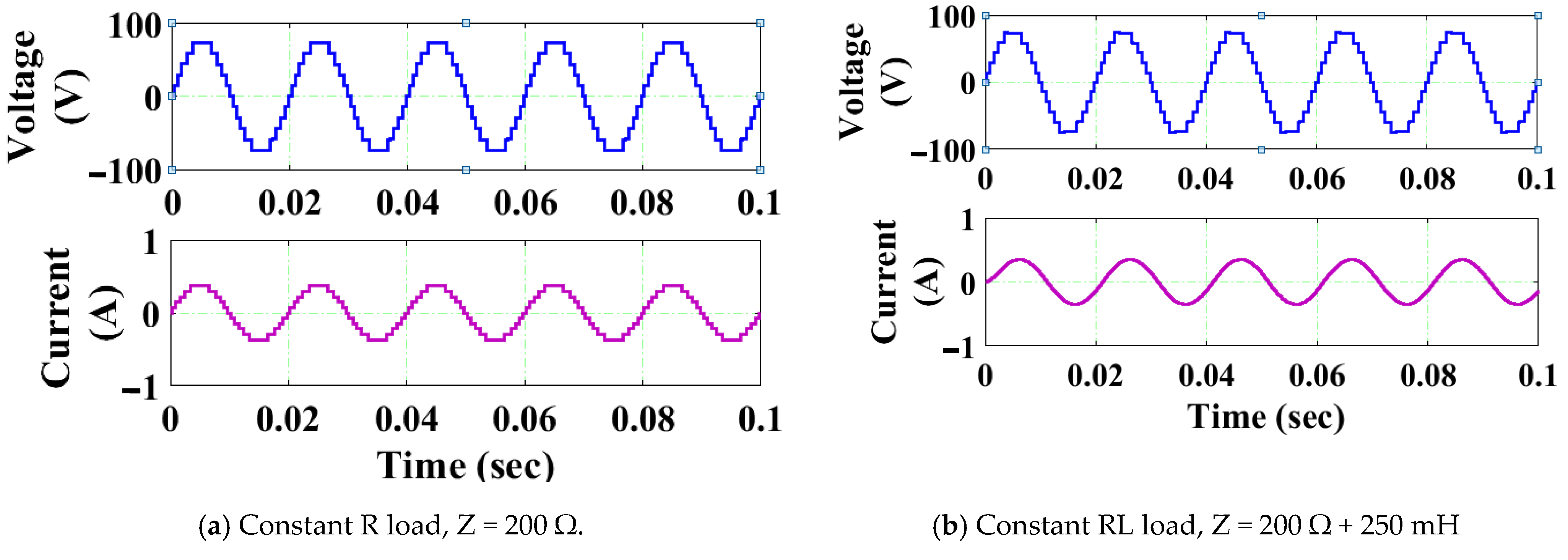
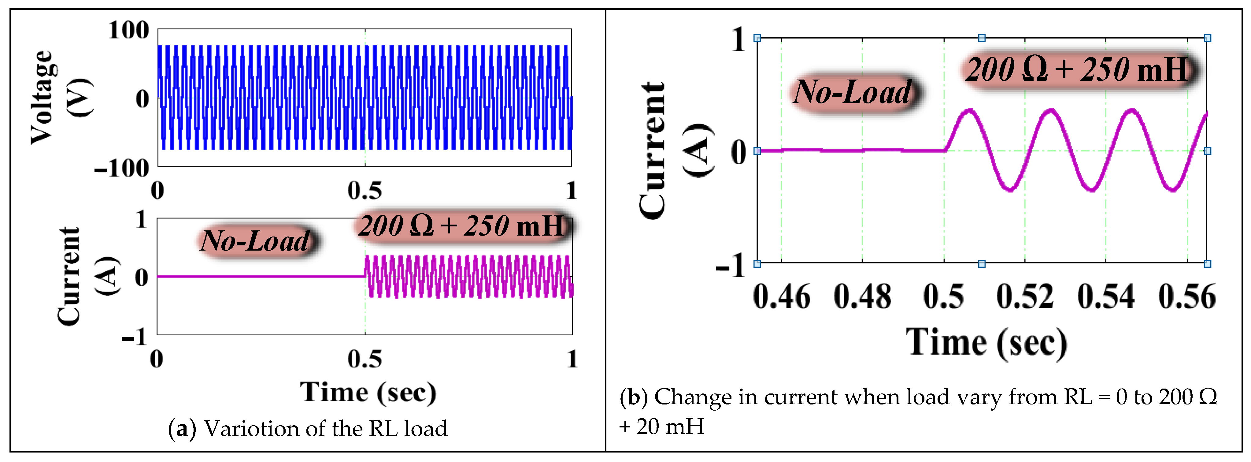
6.1.1. Constant R and RL Load

Figure 7 represents the simulation results for a constant load (R and RL load). The voltage and current waveforms are recorded and displayed here. Figure 7a shows the output voltage and current waveforms for Z = 200 Ω. As it can be seen, the current is in phase with the voltage. The second constant loading result was taken for Z = 200 Ω + 250 mH, which is shown in Figure 7b. Due to the inductive load, the current waveform becomes smoother and it is also displaced in phase with the load voltage.

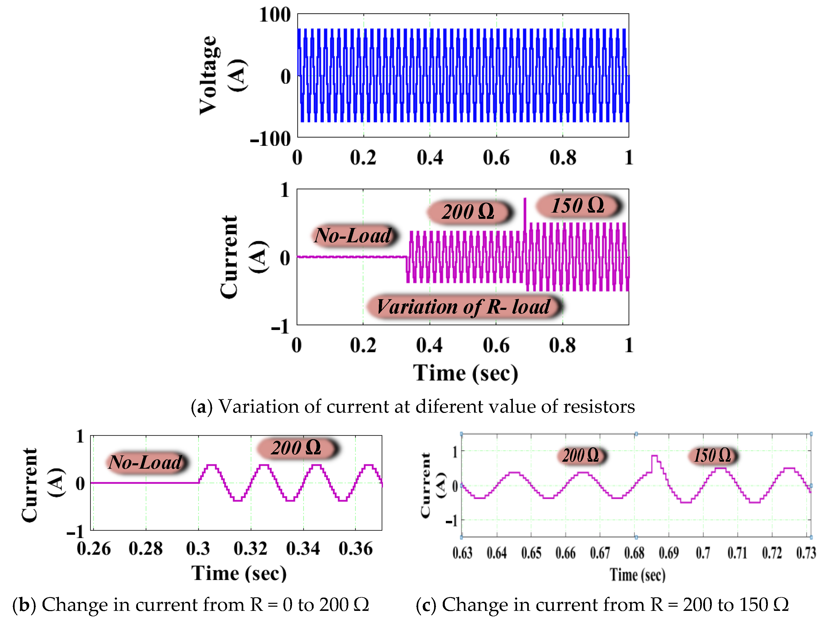
6.1.2. Variable R and RL Load

To analyze the topology in a dynamic loading situation, the results were analyzed for changing load conditions. Figure 8 and Figure 9 depicts the load voltage and current waveforms for alteration in R and RL load, respectively. In Figure 8a, from a no-load condition, the load was first changed to Z = 200 Ω and then to Z = 200 Ω. It is visible from the current waveform that the magnitude is varied at the instants of load changing. However, to provide a close view, Figure 8b,c are included, showing the load changing instants from no-load to Z = 200 Ω and from Z = 200 Ω to Z = 100 Ω, respectively. The value of current increase with the decrease in the load. Similarly, the variation in RL load has also been shown in Figure 9a in which load is varied from no load to Z = 200 Ω + 250 mH. The closer view is given in Figure 9b in which output current can be seen to appear just after the change in load.

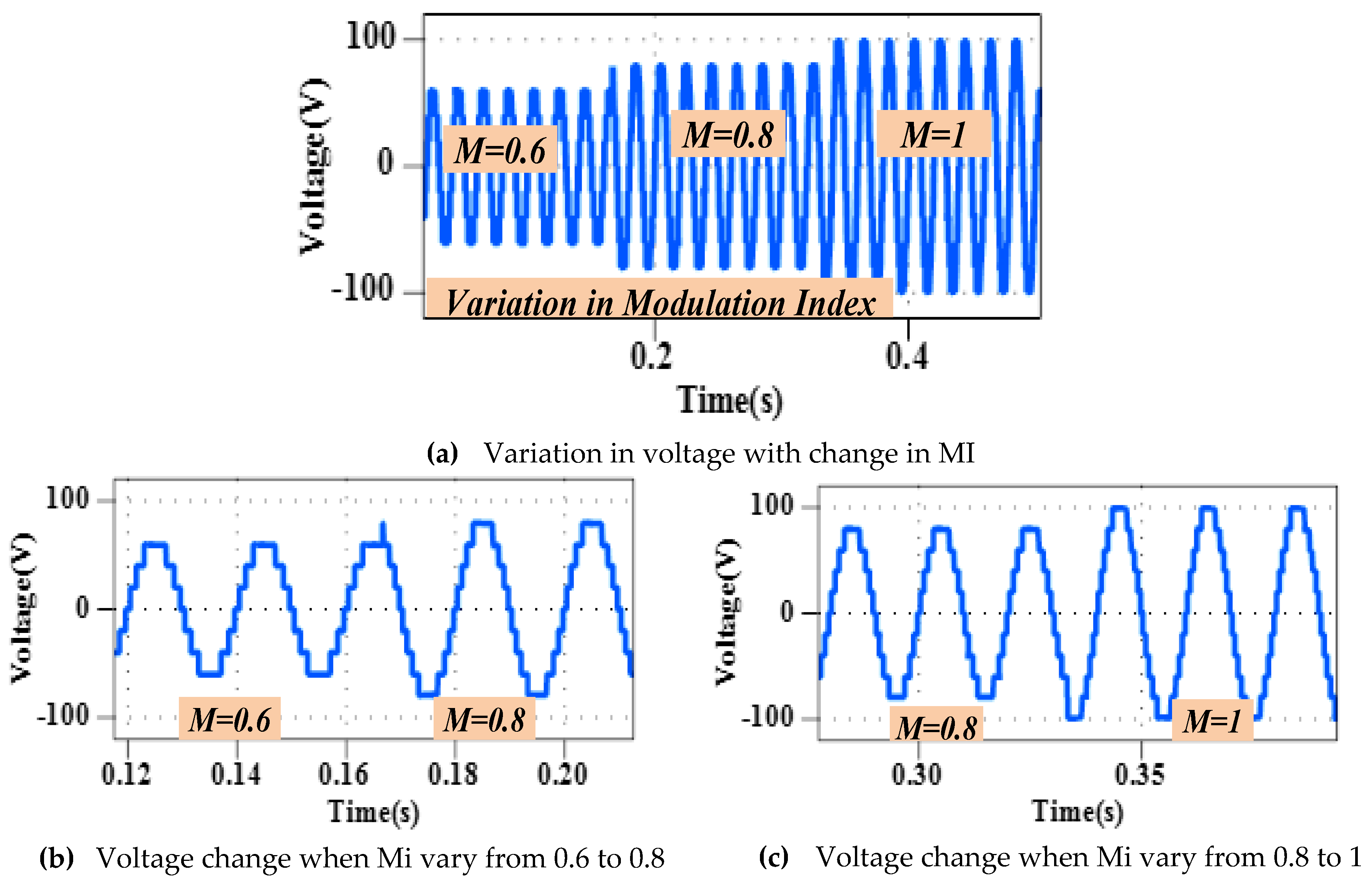
6.1.3. Variation in Modulation Index

Another dynamic condition that is taken into consideration is the change in the modulation index. Modulation Index (M) is the ratio of the modulating signal voltage to the career voltage. The value of the modulation index lies between 0 and 1. The proposed topology is analyzed with the variation of modulation index and observed the output voltage waveform. From Figure 10, we find that the output voltage levels are reduced when we move from m = 1 to 0.6 via 0.8. For M = 1 we have 11 levels, for M = 0.8 we have nine levels and for M = 0.6 we have seven levels.

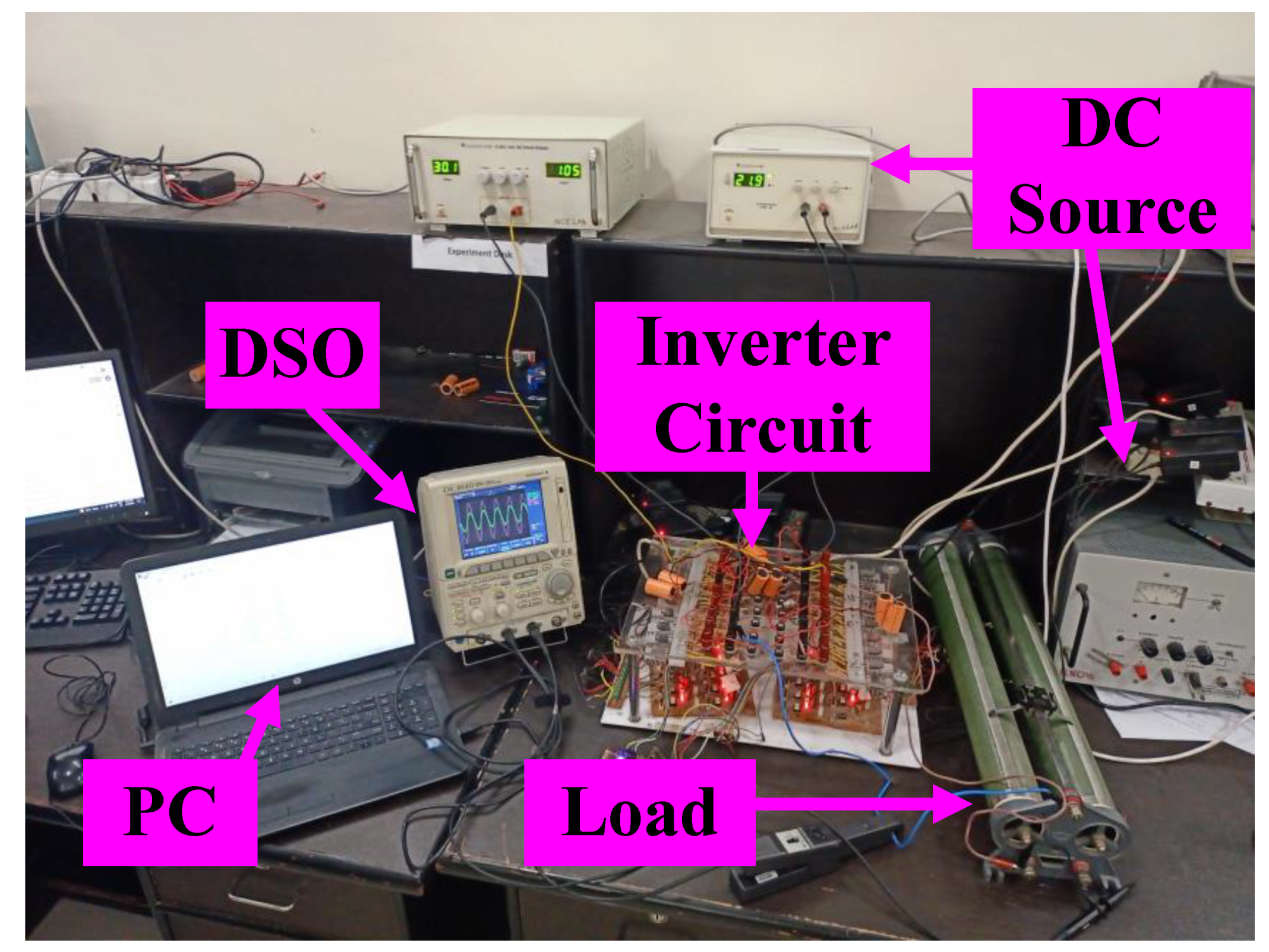
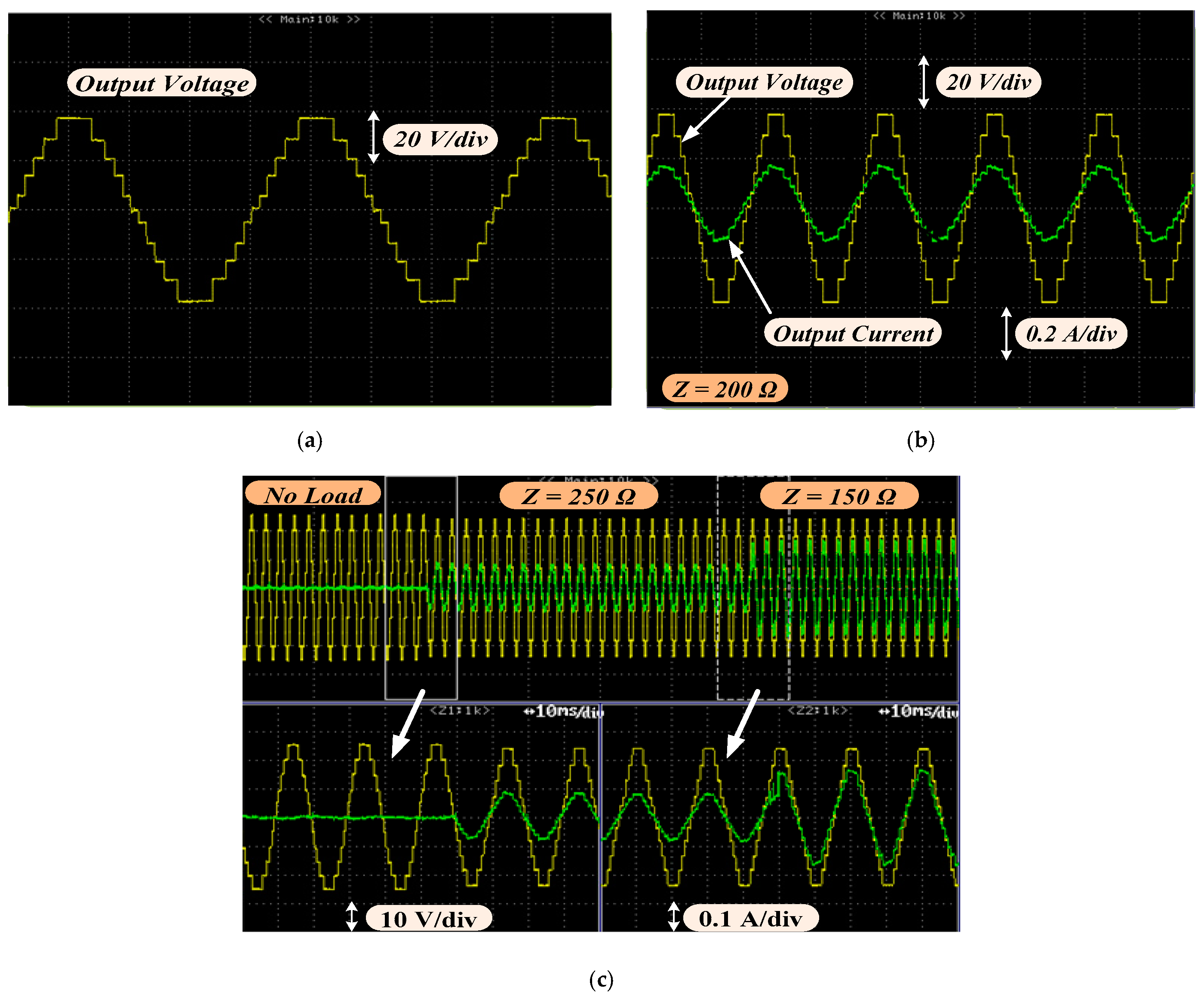
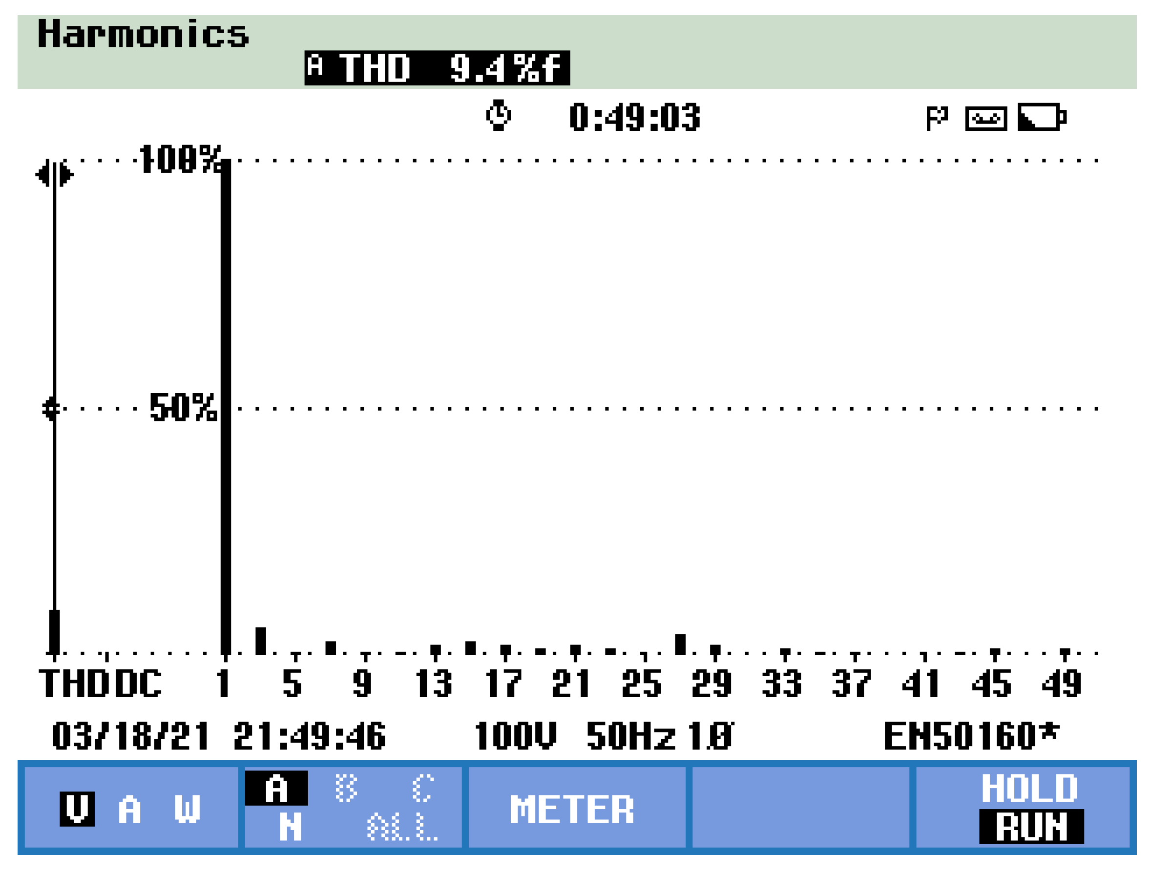
6.2. Hardware Implementation

A prototype of the proposed circuit is developed in the laboratory environment, as shown in Figure 11. The FGA25N120 IGBT is used as power semiconductor switches for the proposed hardware topology. A C2000 LAUNCHPAD XL TMS320F28379D is used to generate control signals. With the help of the TLP 250H driving circuit, the IGBTs are fired. Two Scientech DC sources are used as the DC source for the prototype. The value of 200 Ω is taken as a resistive load. A Yokogawa DL 1640 digital oscilloscope is used to display voltages and current waveform. A typical block diagram of the circuit implementation is shown in Figure 12. It includes a TLP250H based driver circuit, and control logic has been implemented in TMS320F28379D.
These output voltage waveforms with 80 V as peak magnitude are shown in Figure 13a in which the different voltage levels are clearly visible. Figure 13b displays the load waveforms (voltage and current) for a resistive load i.e., Z = 200 Ω in which the two waveforms can be seen to be in phase with each other.
Figure 13c shows the variation in load from no load to 250 Ω to 150 Ω. A close view of the two load-changing moments have also been provided to see the change in current magnitude. As the load changes from Z = 250 Ω to Z = 150 Ω, the increase in current magnitude is visible from the given waveforms. The states are stable, and also, in this case, the phase displacement between the voltage and current is zero.
The experimental THD in the load voltage measured from the power analyzer is 9.4% for a modulation index equal to 1. It is shown in Figure 14.

7. Conclusions

This paper presented and discussed a reduced switching components step-up multilevel inverter (RSCS-MLI). The topology converted the DC voltages in sinusoidal waves with a THD of 9.4%. The NLC modulation techniques were used to provide the pulses to the switches. The simulation of the model was developed in an environment of MATLAB2018a and the thermal analysis was completed in the PLECS environment. A prototype was developed in the laboratory. The simulation results were experimentally verified. A comparative evaluation of performance parameters has also been completed to validate the proposed topology.

Author Contributions

Conceptualization, M.W. and A.S.; formal analysis, M.W., A.S. and Z.S.; funding acquisition, S.A., A.M.A.-S. and J.H.; investigation, M.W., A.S., Z.S., M.T. and J.H.; methodology, M.W., A.S., Z.S. and M.T.; project administration, S.A.; supervision, A.S.; writing—original draft, M.W., A.S. and Z.S.; writing—review and editing, M.T., S.A., A.M.A.-S. and J.H. All authors have read and agreed to the published version of the manuscript.

Funding

The authors extend their appreciation to King Saud University for funding this work through Researchers Supporting Project number (RSP-2021/387), King Saud University, Riyadh, Saudi Arabia.

Institutional Review Board Statement

Not applicable.

Informed Consent Statement

Not applicable.

Data Availability Statement

Not applicable.

Conflicts of Interest

The authors declare no conflict of interest.

References

  1. Kumari, M.; Siddique, M.D.; Sarwar, A.; Mekhilef, S.; Tariq, M. A twice boost nine-level switched-capacitor multilevel (2B-9L-SCMLI) inverter with self-voltage balancing capability. Int. J. Circ. Theor. Appl. 2021, 49, 1–15. [Google Scholar] [CrossRef]
  2. Sarwer, Z.; Siddique, M.D.; Iqbal, A.; Sarwar, A.; Mekhilef, S. An improved asymmetrical multilevel inverter topology with reduced semiconductor device count. Int. Trans. Electr. Energ. Syst. 2020, 30, e12587. [Google Scholar] [CrossRef]
  3. Beig, A.R.; Ranganathan, V.T. Influence of placement of small space vectors on the performance of PWM techniques for three level inverters. In Proceedings of the IECON’03 29th Annual Conference of the IEEE Industrial Electronics Society, Roanoke, VA, USA, 2–6 November 2003; Volume 3, pp. 2764–2770. [Google Scholar] [CrossRef] [Green Version]
  4. Sathik, M.J.; Krishnasamy, V. An assessment of recent multilevel inverter topologies with reduced power electronics components for renewable applications. Renew. Sustain. Energy Rev. 2017, 82, 3379–3399. [Google Scholar]
  5. Prabaharan, N.; Palanisamy, K. A comprehensive review on reduced switch multilevel inverter topologies, modulation techniques and applications. Renew. Sustain. Energy Rev. 2017, 76, 1248–1282. [Google Scholar] [CrossRef]
  6. Kumari, M.; Siddique, M.D.; Sarwar, A.; Tariq, M.; Mekhilef, S.; Iqbal, A. Recent trends and review on switched-capacitor-based single-stage boost multilevel inverter. Int. Trans. Electr. Energ. Syst. 2021, 31, e12730. [Google Scholar] [CrossRef]
  7. Ounejjar, Y.; Al-Haddad, K.; Dessaint, L.A. A novel six-band hysteresis control for the packed U cells seven-level converter: Experimental validation. IEEE Trans. Ind. Electron. 2012, 59, 3808–3816. [Google Scholar] [CrossRef]
  8. Siddique, M.D.; Mekhilef, S.; Rawa, M.; Wahyudie, A.; Chokaev, B.; Salamov, I. Extended Multilevel Inverter Topology with Reduced Switch Count and Voltage Stress. IEEE Access 2020, 8, 201835–201846. [Google Scholar] [CrossRef]
  9. Siddique, M.D.; Mekhilef, S.; Shah, N.M.; Memon, M.A. Optimal Design of a New Cascaded Multilevel Inverter Topology with Reduced Switch Count. IEEE Access 2019, 7, 24498–24510. [Google Scholar] [CrossRef]
  10. Priyadarshi, A.; Kar, P.K.; Karanki, S.B. A Single Source Transformer-Less Boost Multilevel Inverter Topology with Self-Voltage Balancing. IEEE Trans. Ind. Appl. 2020, 56, 3954–3965. [Google Scholar] [CrossRef]
  11. Prasanth, S.R.; John, M.; Rao, S. 11-Level Multilevel Inverter with Reduced Number of Switches using Level Shift Modulation. Int. J. Mod. Trends Sci. Technol. 2017, 3, 53–58. [Google Scholar]
  12. Ganesan, R.G.; Shankar, R.; Bhaskar, M.; Narayanan, K. Switched Capacitor Based Multilevel Boost Inverter for Smart Grid Applications. In Proceedings of the 2019 IEEE Innovative Smart Grid Technologies-Asia (ISGT Asia), Chengdu, China, 21–24 May 2019; pp. 3902–3907. [Google Scholar] [CrossRef]
  13. Arif, M.S.B.; Mustafa, U.; Siddique, M.D.; Ahmad, S.; Iqba, A.; Ashique, R.H.; Ayob, S.b. An improved asymmetrical multi-level inverter topology with boosted output voltage and reduced components count. IET Power Electron. 2021, 14, 1–15. [Google Scholar] [CrossRef]
  14. Vasudevamurthy, S.; Somashekara, G. Simulation of 11-level Inverter with Reduced Number of Power Switches for R and RL load. IJAREEIE 2017, 6, 3458–3467. [Google Scholar]
  15. Khan, M.N.H.; Forouzesh, M.; Siwakoti, Y.P.; Li, L.; Blaabjerg, F. Switched Capacitor Integrated (2n + 1)-Level Step-Up Single-Phase Inverter. IEEE Trans. Power Electron. 2020, 35, 8248–8260. [Google Scholar] [CrossRef]
  16. Sarwer, Z.; Sarwar, A.; Zaid, M.; Tariq, M.; Ali, M.; Arif, M.S.B. A switched capacitor multilevel inverter with self voltage balancing capability. In Proceedings of the 2020 IEEE International Conference on Power Electronics, Drives and Energy Systems (PEDES), Jaipur, India, 16–19 December 2020. [Google Scholar]
  17. Sarwer, Z.; Siddique, M.D.; Iqbal, A.; Sarwar, A.; Rahman, K.; Mekhilef, S. Seven-level switched-capacitor based multilevel inverter with lesser number of power electronic components and reduced voltage stress. In Proceedings of the 2020 IEEE International Conference on Power Electronics, Drives and Energy Systems (PEDES), Jaipur, India, 16–19 December 2020. [Google Scholar]
  18. Mahdavi, A.; Abbaszadeh, K.; Mardakheh, N.A. A Boost Switched-Capacitor Multilevel Inverter with Self-Balance and Inductive-load Ability. In Proceedings of the 2020 11th Power Electronics, Drive Systems, and Technologies Conference (PEDSTC), Tehran, Iran, 4–6 February 2020. [Google Scholar]
  19. Kumar, A.R.; Thangavelusamy, D. A modified nearest level modulation scheme for symmetric and asymmetric configurations of cascaded H-bridge inverter. Int. J. Electr. Eng. Educ. 2019, 32, 471–481. [Google Scholar] [CrossRef]
  20. Samadaei, E.; Kaviani, M.; Bertilsson, K. A 13-levels module (K-Type) with two DC sources for multilevel inverters. IEEE Trans. Ind. Electron. 2019, 66, 5186–5196. [Google Scholar] [CrossRef]
  21. Barzegarkhoo, R.; Moradzadeh, M.; Zamiri, E.; Kojabadi, H.M.; Blaabjerg, F. A New Boost Switched-Capacitor Multilevel Converter with Reduced Circuit Devices. IEEE Trans. Power Electron. 2018, 33, 6738–6754. [Google Scholar] [CrossRef]
  22. Arun, N.M.; Noel, M. Crisscross switched multilevel inverter using cascaded semi-half-bridge cells. IET Power Electron. 2018, 11, 23–32. [Google Scholar] [CrossRef] [Green Version]
  23. Mokhberdoran, A.; Ajami, A. Symmetric and asymmetric design and implementation of new cascaded multilevel inverter topology. IEEE Trans. Power Electron. 2014, 29, 6712–6724. [Google Scholar] [CrossRef]
  24. Hussain, M.R.; Sarwar, A.; Siddique, M.D.; Mekhilef, S.; Ahmad, S.; Sharaf, M.; Zaindin, M.; Firdausi, M. A Novel Switched-Capacitor Multilevel Inverter Topology for Energy Storage and Smart Grid Applications. Electronics 2020, 9, 1703. [Google Scholar] [CrossRef]
  25. Siddique, M.D.; Iqbal, A.; Sathik, M.J.; Mekhilef, S.; Almakhles, D.J. Design and implementation of a new unity gain nine-level active neutral point clamped multilevel inverter topology. IET Power Electron. 2020, 13, 3204–3208. [Google Scholar] [CrossRef]
  26. Arif, M.S.B.; Mustafa, U.; Ayob, S.B.M.; Rodriguez, J.; Nadeem, A.; Abdelrahem, M. Asymmetrical 17-level Inverter Topology with Reduced Total Standing Voltage and Device Count. IEEE Access 2021, 9, 69710–69723. [Google Scholar] [CrossRef]
Figure 1. Proposed RSCS-MLI.
Processes 09 01948 g001
Figure 2. Conduction paths for different voltage levels of the proposed topology.
Processes 09 01948 g002
Figure 3. Voltage stress on switches in the proposed topology.
Processes 09 01948 g003
Figure 4. NLC Switching Scheme.
Processes 09 01948 g004
Figure 5. Thermal Description for Different Losses for Different Temperature in °C.
Processes 09 01948 g005
Figure 6. (a) Conduction Loss, (b) Switching Loss, (c) Efficiency Variation with Load.
Processes 09 01948 g006
Figure 7. Simulation Results for Constant Loading Condition.
Processes 09 01948 g007
Figure 8. Output Voltage and Current with Variation of the R-Load.
Processes 09 01948 g008
Figure 9. Output Voltage and Current with Variation of the RL Load.
Processes 09 01948 g009
Figure 10. Output voltage with variation in Modulation Index.
Processes 09 01948 g010
Figure 11. Laboratory Prototype of the Proposed Topology.
Processes 09 01948 g011
Figure 12. Circuit Used for the Implementation of the Topology.
Processes 09 01948 g012
Figure 13. Hardware results of the proposed topology (a) Output Voltage (b) Voltage and current waveform for resistive load (c) Variation of the Current waveform for change in the R-Load.
Processes 09 01948 g013
Figure 14. Hardware results for total harmonic distortion.
Processes 09 01948 g014
Table 1. Switching Table Along with Output Voltage.
VoSXS1S2S3S4SBSYP1P2P3P4
Positive Voltage Levels2.5 VDC10101101010
2 VDC10111001000
1.5 VDC10110001001
VDC00111011000
0.5 VDC00110011001
Zero Voltage Level001111010000
Negative Voltage Levels−0.5 VDC01001010110
−VDC01000010111
−1.5 VDC01010110101
−2 VDC11000000111
−2.5 VDC11010100101
Table 2. Comparative Evaluation.
TopologyNswitchNdiodeNTNL/NTNsourceNcapNLTSVP.U.
[8]8081.430119.6
[9]8081.430115.6
[10]109190.619118
[18]121130.822116.4
[19]115160.750115
[20]140140.922136.33
[25]104140.61497
Proposed111120.921115
Table 3. Simulation Parameters.
ComponentsSpecification
DC voltage source (2)20V, 40V
Fundamental frequency50 Hz
Capacitor3000 µF
LoadR = 100 Ω, 200 Ω, L = 250 mH
Publisher’s Note: MDPI stays neutral with regard to jurisdictional claims in published maps and institutional affiliations.

