Optimal Cooling System Design for Increasing the Crystal Growth Rate of Single-Crystal Silicon Ingots in the Czochralski Process Using the Crystal Growth Simulation


Abstract
:1. Introduction
2. Mathematical Modeling and Experiment
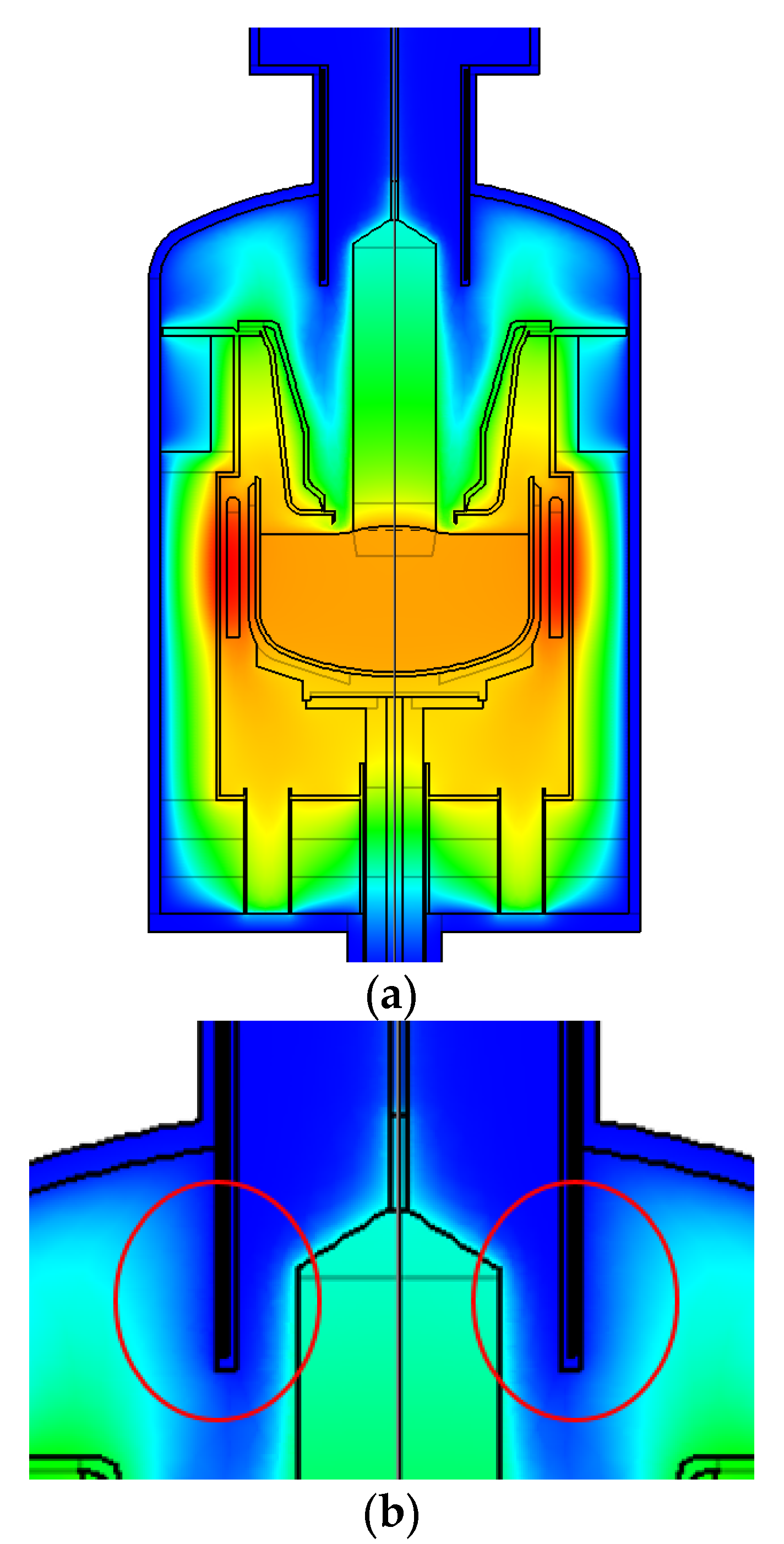
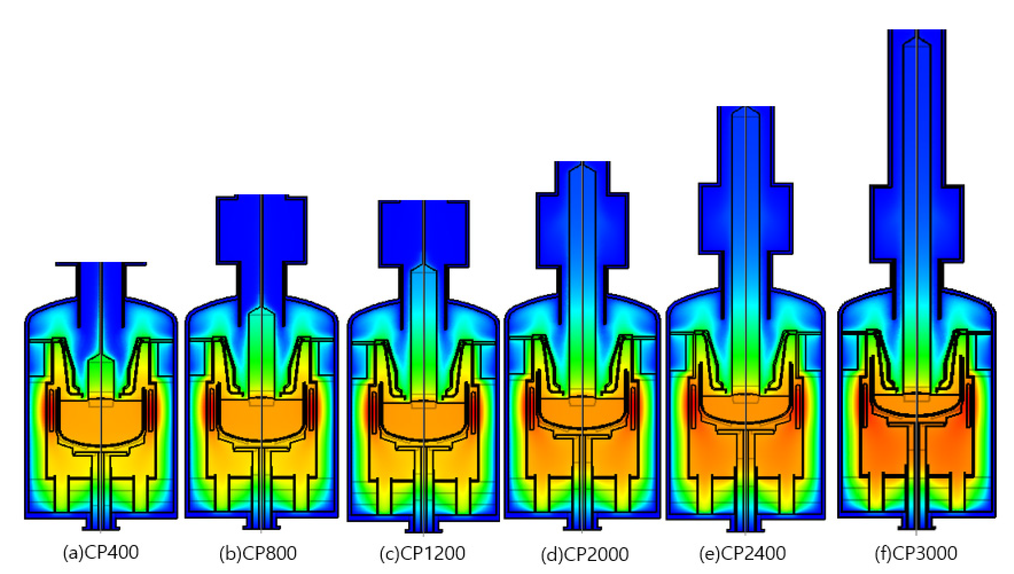
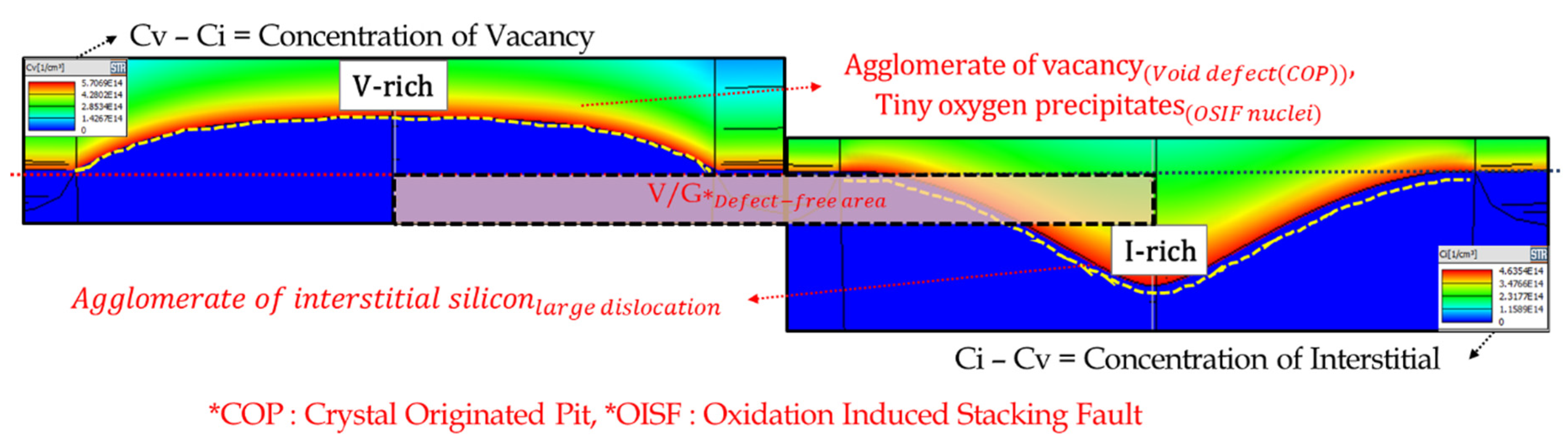
3. Results and Discussions
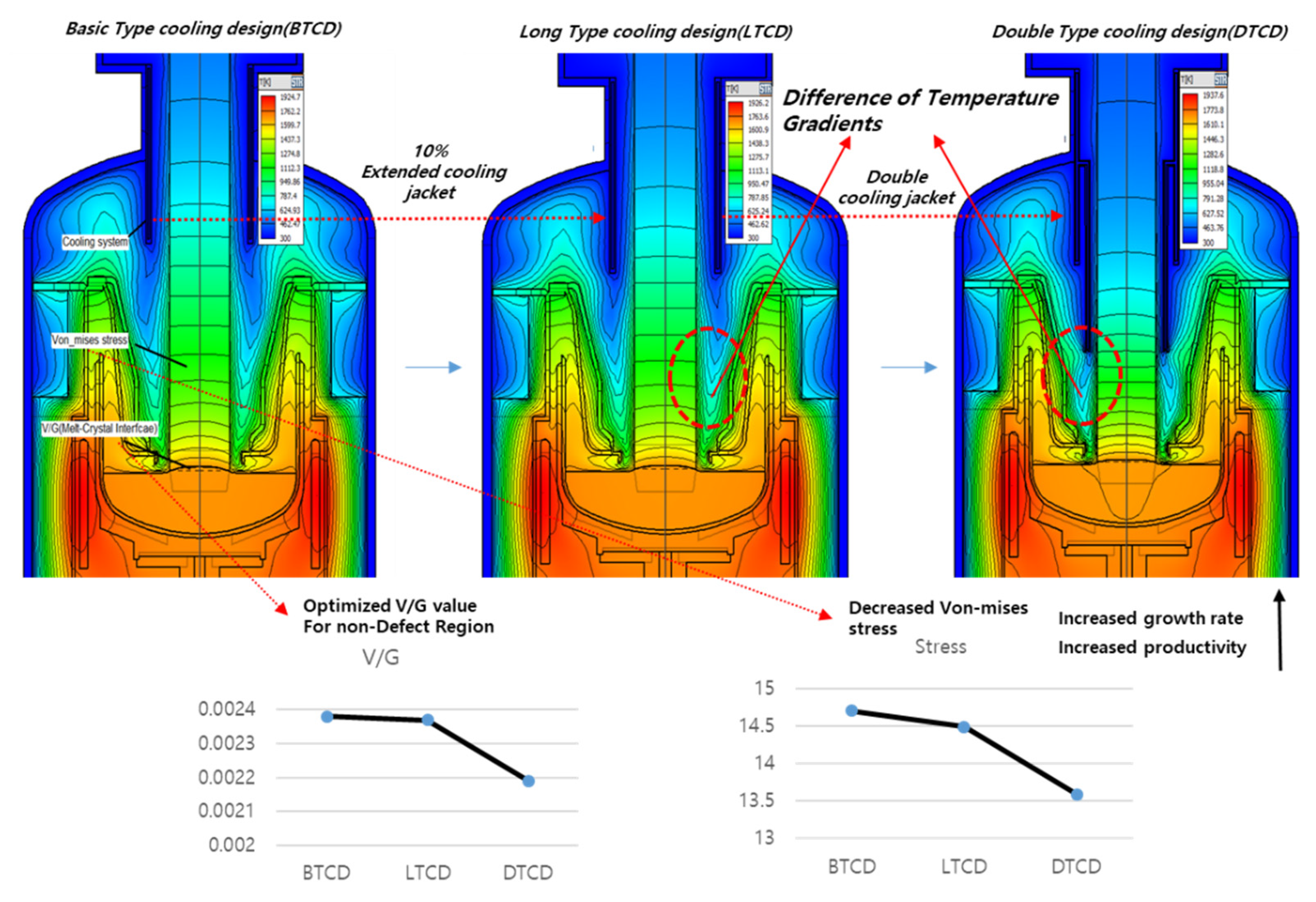
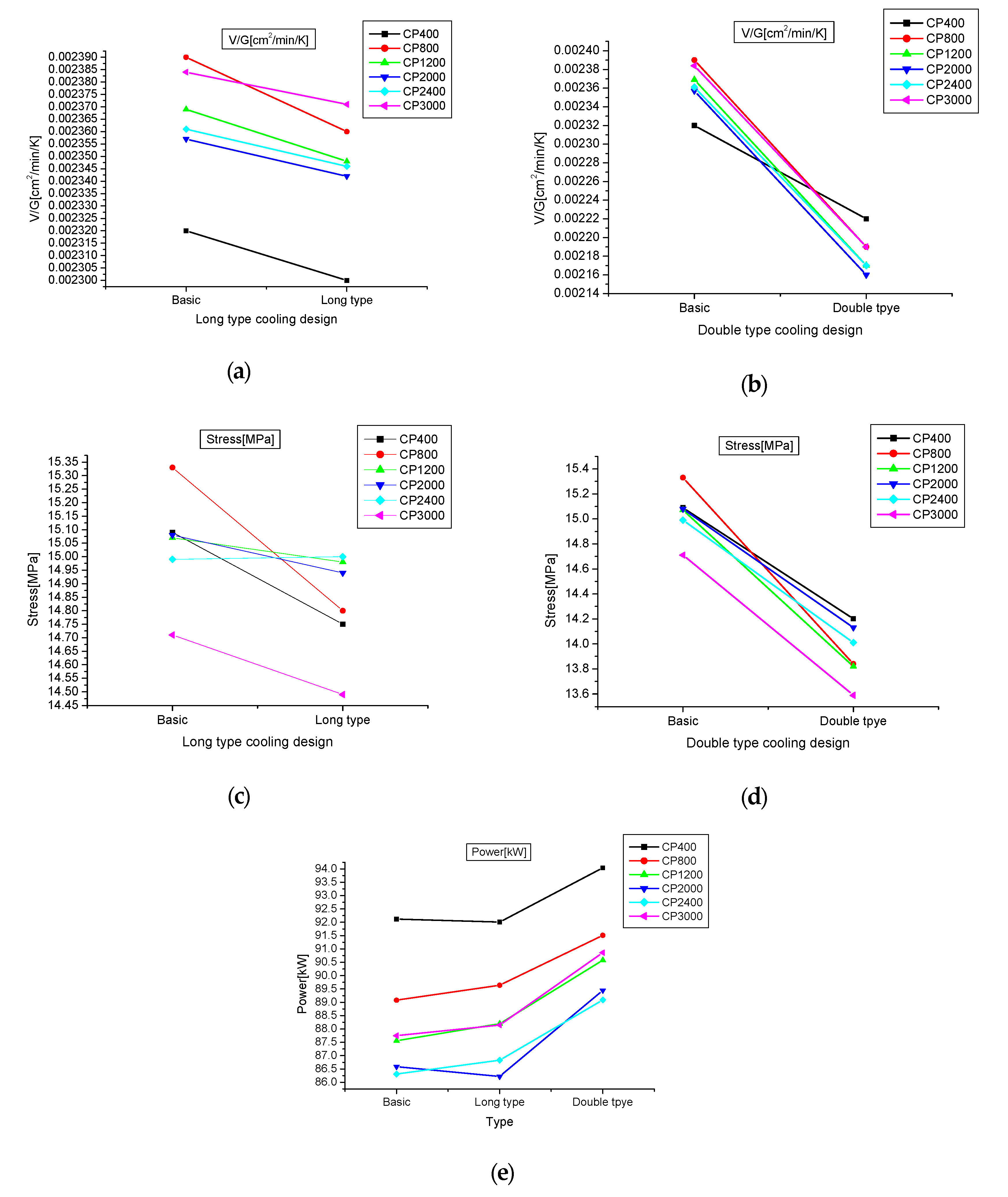
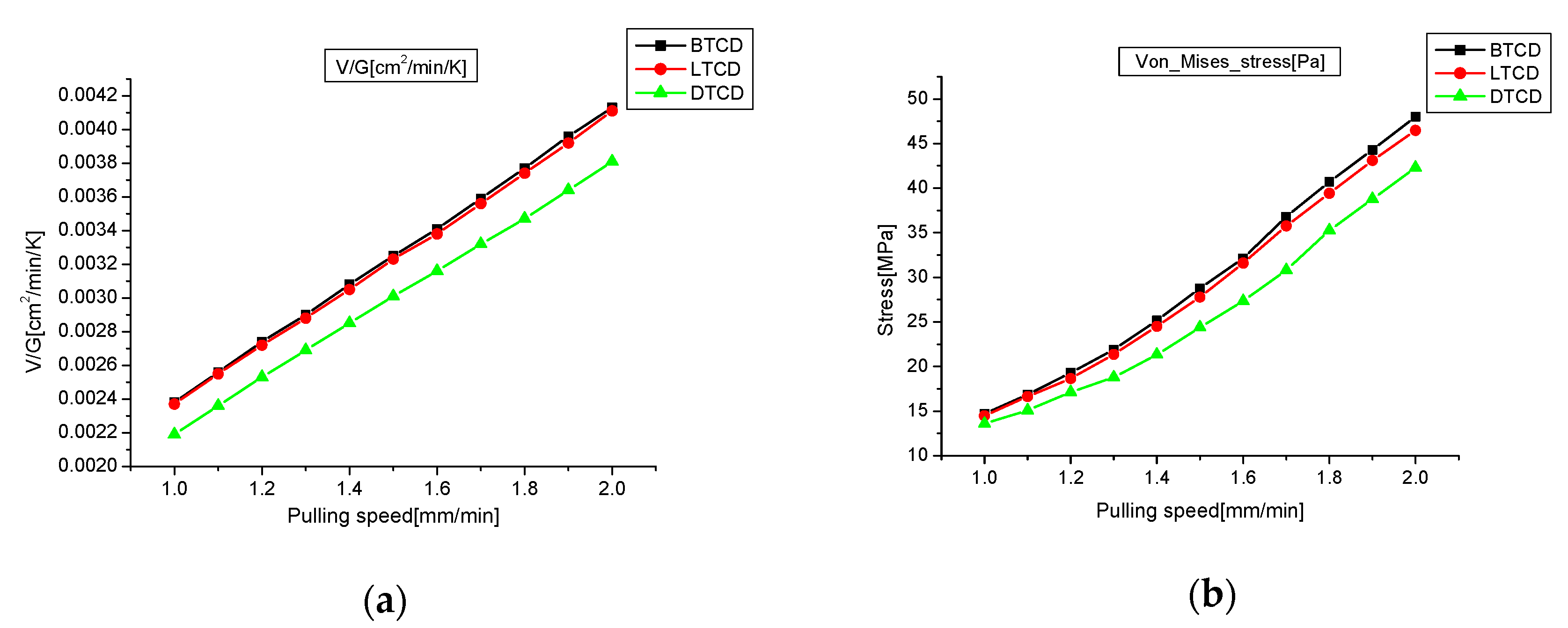
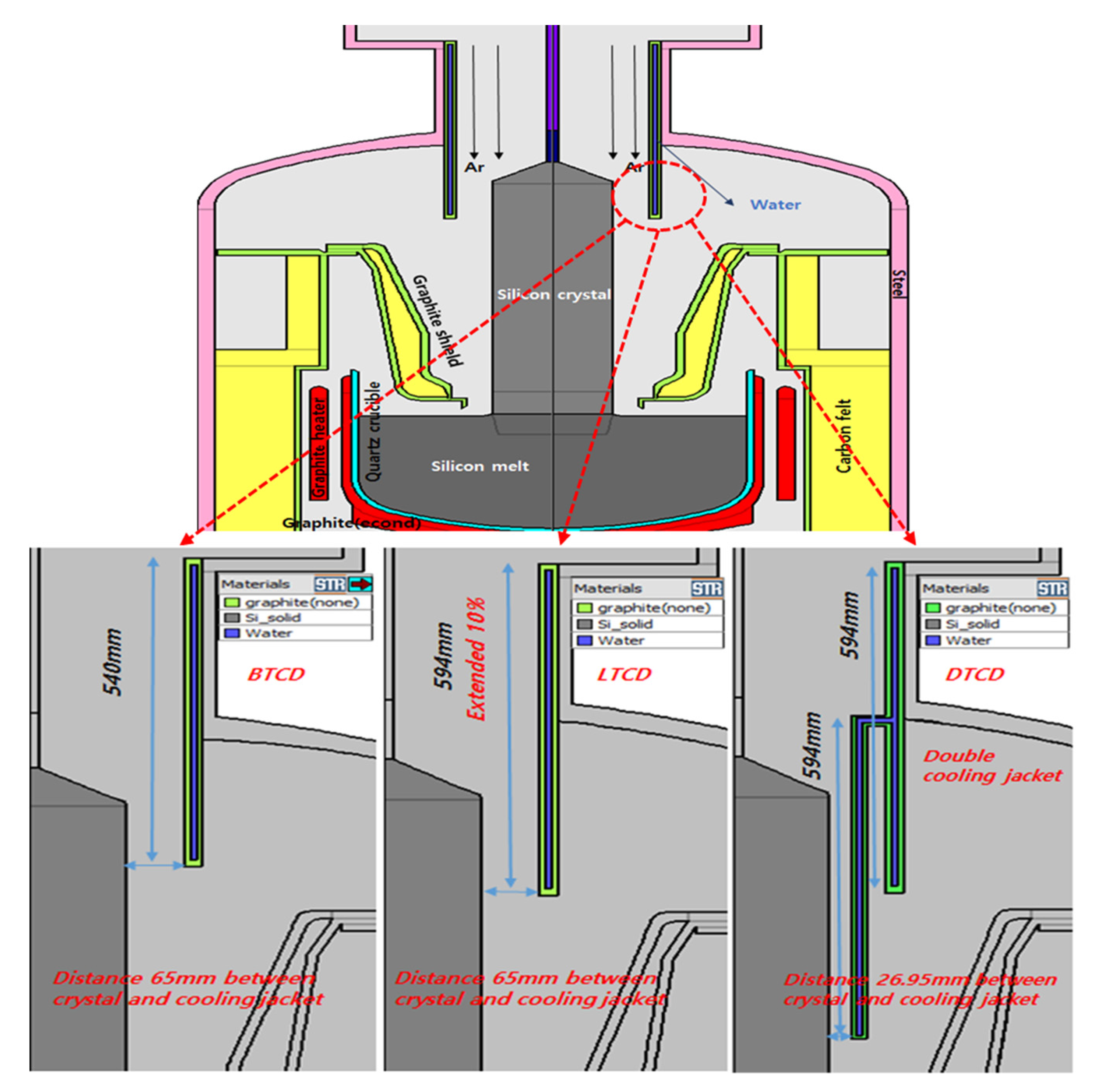
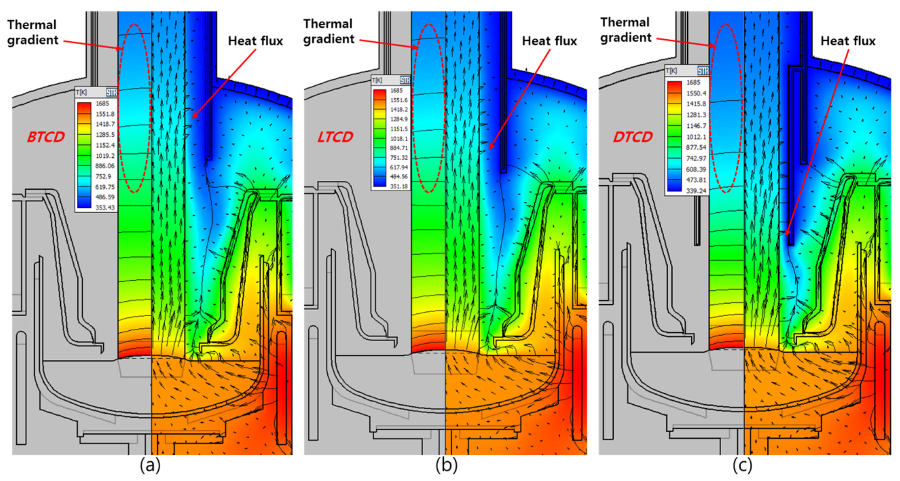
Cooling System Length Adjustment and Dual-System Design
4. Conclusions
Author Contributions
Funding
Acknowledgments
Conflicts of Interest
Software
References
- Deai, H.; Iwasaki, T.; Ikematsu, Y.; Kawakami, K.; Harada, H.; Matsumura, A. Influence of crystal originated particles on gate oxide breakdown. Jpn. J. Appl. Phys. 1996, 35, L1476. [Google Scholar] [CrossRef]
- Friedrich, J.; von Ammon, W.; Müller, G. Czochralski growth of silicon crystals. In Handbook of Crystal Growth; Elsevier: Amsterdam, The Netherlands, 2014; pp. 45–104. [Google Scholar]
- Czochralski, J. A new method for the measurement of the crystallization rate of metals. Z. für Phys. Chem. 1918, 92, 219–221. [Google Scholar]
- Von Ammon, W.; Gelfgat, Y.; Gorbunov, L.; Muhlbauer, A.; Muiznieks, A.; Makarov, Y.; Virbulis, J.; Muller, G. Application of magnetic fields in industrial growth of silicon single crystals. In Proceedings of the joint 15th Riga and 6th PAMIR Conf. on Fundamental and Applied MHD, Rigas, Latvia, 27 June–1 July 2005; pp. 41–45. [Google Scholar]
- Kalaev, V.; Sattler, A.; Kadinski, L. Crystal twisting in Cz Si growth. J. Cryst. Growth 2015, 413, 12–16. [Google Scholar] [CrossRef]
- Dornberger, E.; Ammon, W. Silicon materials science and technology. J. Electrochem. Soc. 1996, 143, 1636. [Google Scholar]
- Voronkov, V.; Falster, R. Vacancy-type microdefect formation in Czochralski silicon. J. Cryst. Growth 1998, 194, 76–88. [Google Scholar] [CrossRef]
- Rozgonyi, G.; Deysher, R.; Pearce, C. The identification, annihilation, and suppression of nucleation sites responsible for silicon epitaxial stacking faults. J. Electrochem. Soc. 1976, 123, 1910. [Google Scholar] [CrossRef]
- Shockley, W.; Read, W., Jr. Statistics of the recombinations of holes and electrons. Phys. Rev. 1952, 87, 835. [Google Scholar] [CrossRef]
- Forrest, E.C.; Hu, L.-W.; Buongiorno, J.; McKrell, T.J. Convective heat transfer in a high aspect ratio minichannel heated on one side. J. Heat Transf. 2016, 138, 21704–21710. [Google Scholar] [CrossRef]
- Kalaev, V.; Lukanin, D.; Zabelin, V.; Makarov, Y.N.; Virbulis, J.; Dornberger, E.; Von Ammon, W. Calculation of bulk defects in CZ Si growth: Impact of melt turbulent fluctuations. J. Cryst. Growth 2003, 250, 203–208. [Google Scholar] [CrossRef]
- Kalaev, V.; Evstratov, I.Y.; Smirnov, E.; Zhmakin, A.; Makarov, Y.N. Numerical modeling of Czochralski silicon crystal growth. In Proceedings of the European Congress on Computational Methods in Applied Sciences and Engineering––ECCOMAS, Barcelona, Spain, 11–14 September 2000; pp. 1–9. [Google Scholar]
- Pohl, J.; Müller, M.; Seidl, A.; Albe, K. Formation of parallel (1 1 1) twin boundaries in silicon growth from the melt explained by molecular dynamics simulations. J. Cryst. Growth 2010, 312, 1411–1415. [Google Scholar] [CrossRef]
- Noghabi, O.A.; M’Hamdi, M.; Jomâa, M. Effect of crystal and crucible rotations on the interface shape of Czochralski grown silicon single crystals. J. Cryst. Growth 2011, 318, 173–177. [Google Scholar] [CrossRef]
- Liu, L.; Kakimoto, K. Effects of crystal rotation rate on the melt–crystal interface of a CZ-Si crystal growth in a transverse magnetic field. J. Cryst. Growth 2008, 310, 306–312. [Google Scholar] [CrossRef]
- Voronkov, V.; Falster, R. Vacancy and self-interstitial concentration incorporated into growing silicon crystals. J. Appl. Phys. 1999, 86, 11, 5975–5982. [Google Scholar] [CrossRef]
- Kamiyama, E.; Sueoka, K.; Vanhellemont, J. Ab initio study of vacancy and self-interstitial properties near single crystal silicon surfaces. J. Appl. Phys. 2012, 111, 8. [Google Scholar] [CrossRef]
- Prostomolotov, A.; Verezub, N.; Mezhennii, M.; Reznik, V.Y. Thermal optimization of CZ bulk growth and wafer annealing for crystalline dislocation-free silicon. J. Cryst. Growth 2011, 318, 187–192. [Google Scholar] [CrossRef]
- Sim, B.-C.; Jung, Y.-H.; Lee, H.-W. Effect of the ingot cooling on the grown-in defects in silicon Czochralski growth. Jpn. J. Appl. Phys. 2009, 48, 105503. [Google Scholar] [CrossRef]
- Zhao, W.; Liu, L. Control of heat transfer in continuous-feeding Czochralski-silicon crystal growth with a water-cooled jacket. J. Cryst. Growth 2017, 458, 31–36. [Google Scholar] [CrossRef]
- Liu, X.; He, L.J.; Bai, Z.; Shuang, Y.; Zhou, C.; Shao, J. Numerical Analysis on Cooling Process of Monocrystal Silicon Rod Manufactured with Czochralski Method. Appl. Mech. Mater. 2012, 217–219, 1425–1428. [Google Scholar] [CrossRef]
- Miyazaki, N.; Uchida, H.; Munakata, T.; Fujioka, K.; Sugino, Y. Thermal stress analysis of silicon bulk single crystal during Czochralski growth. J. Cryst. Growth 1992, 125, 102–111. [Google Scholar] [CrossRef]
- Mukaiyama, Y.; Sueoka, K.; Maeda, S.; Iizuka, M.; Mamedov, V.M. Numerical analysis of effect of thermal stress depending on pulling rate on behavior of intrinsic point defects in large-diameter Si crystal grown by Czochralski method. J. Cryst. Growth 2020, 531, 12533. [Google Scholar] [CrossRef]
- Gopu, V.K. Validity of distortion-energy-based strength criterion for timber members. J. Struct. Eng. 1987, 113, 2475–2487. [Google Scholar] [CrossRef]
- Kulkarni Milind, S.; Holzer Joseph, C.; Ferry Lee, W. The agglomeration dynamics of self-interstitials in growing Czocharlski silicon crystals. J. Cryst. Growth 2005, 282, 353–368. [Google Scholar] [CrossRef]
- Voronkov, V.; Falster, R. Intrinsic point defects and impurities in silicon crystal growth. J. Electrochem. Soc. 2002, 149, G167. [Google Scholar] [CrossRef]
- Kulkarni Milind, S. Defect dynamics in the presence of oxygen in growing Czochralski silicon crystals. J. Cryst. Growth 2007, 303, 438–448. [Google Scholar] [CrossRef]
- Falster, R.; Laczik, Z.; Booker, G.R.; Bhatti, A.R.; Török, P. Defect Engineering in Semiconductor Growth, Processing and Device Technology; Materials Research Society: Pittsburgh, PA, USA, 1992; Volume 26, p. 945. [Google Scholar]
- Voronkov, V.; Falster, R. Grown-in microdefects, residual vacancies and oxygen precipitation bands in Czochralski silicon. J. Appl. Phys. 1999, 204, 462–474. [Google Scholar] [CrossRef]
- Sueoka, K.; Kamiyama, E.; Vanhellemont, J. Theoretical study of the impact of stress on the behavior of intrinsic point defects on large diameter defect-free Si crystals. J. Cryst. Growth 2013, 363, 97–104. [Google Scholar] [CrossRef]
- Jea Gun, P. Advanced Czochralski Single Silicon Crystal Growth: Silicon(<Special Issue>Bulk Crystals for Human Activity in the New Millennium. J. Jpn. Assoc. Cryst. Growth 2000, 27, 14–21. [Google Scholar]
- Kim, J. A Study on Dynamic Heat Flux for 450mm Single Crystal Silicon Growth under Magnetic Fields. Master’s Thesis, Hanyang University, Seoul, Korea, 2007. [Google Scholar]
- Von Ammon, W.; Dornberger, E.; Oelkrug, H.; Weidner, H. The dependence of bulk defects on the axial temperature gradient of silicon crystals during Czochralski growth. J. Cryst. Growth 1995, 151, 273–277. [Google Scholar] [CrossRef]
- Kulkarni Milind, S. Lateral incorporation of vacancies in Czochralski silicon crystals. J. Cryst. Growth 2008, 310, 3183–3191. [Google Scholar] [CrossRef]


| Materials | Heat Capacity (J/kg) | Heat Conductivity (W/m) | Emissivity |
|---|---|---|---|
| Si(crystal) | 1000 | 75.22 | 0.7 |
| Si(melt) | 915 | 66.50 | 0.3 |
| Graphite | 720 | 105.26 | 0.7 |
| Ar | 521 | 3.06 | – |
| Quartz crucible | 1232 | 4 | 0.85 |
| Steel | 438 | 15 | 0.45 |
| Carbon felt | – | 0.02 | 0.9 |
| Water | 4200 | 0.6 | 0.5 |
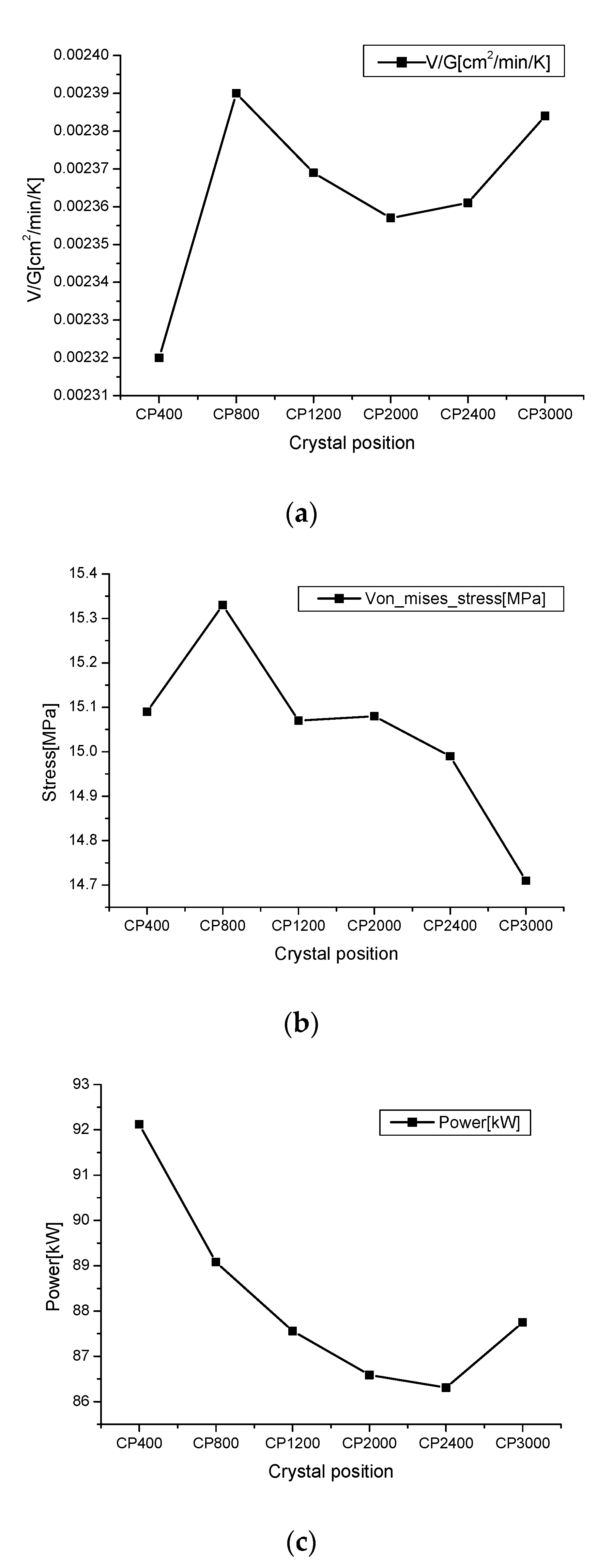
| Crystal Position | V/G (cm2/min/K) (Average) | von Mises Stress (MPa) (Average) | Power (kW) | Crystal Mass (kg) |
|---|---|---|---|---|
| CP400 | 0.00232 | 15.09 | 92.12 | 29.25 |
| CP800 | 0.00239 | 15.33 | 89.08 | 62.41 |
| CP1200 | 0.00236 | 15.07 | 87.56 | 95.77 |
| CP2000 | 0.00235 | 15.08 | 86.59 | 162.52 |
| CP2400 | 0.00236 | 14.99 | 86.31 | 196.60 |
| CP3000 | 0.00238 | 14.71 | 87.75 | 246.07 |
| Type | CP400 | CP800 | CP1200 | CP2000 | CP2400 | CP3000 | |
|---|---|---|---|---|---|---|---|
| V/G (cm2/min/k) | BTCD | 0.00232 | 0.00239 | 0.00236 | 0.00235 | 0.00236 | 0.00238 |
| LTCD | 0.00230 | 0.00236 | 0.00234 | 0.00234 | 0.00234 | 0.00237 | |
| DTCD | 0.00222 | 0.00219 | 0.00217 | 0.00216 | 0.00217 | 0.00219 | |
| von Mises stress (MPa) | BTCD | 15.09 | 15.33 | 15.07 | 15.08 | 14.99 | 14.71 |
| LTCD | 14.75 | 14.80 | 14.98 | 14.94 | 15.00 | 14.49 | |
| DTCD | 14.20 | 13.84 | 13.82 | 14.13 | 14.01 | 13.59 | |
| Power (kW) | BTCD | 92.12 | 89.08 | 87.56 | 86.59 | 86.31 | 87.75 |
| LTCD | 92.01 | 89.64 | 88.20 | 86.22 | 86.83 | 88.15 | |
| DTCD | 94.04 | 91.51 | 90.58 | 89.45 | 89.09 | 90.86 |
| Pulling Speed | V/G (cm2/min/K) | von_Mises_Stress (MPa) | ||||||
|---|---|---|---|---|---|---|---|---|
| BTCD | LTCD | DTCD | Decreasing Rate % | BTCD | LTCD | DTCD | Decreasing Rate % | |
| 1.0 | 0.00238 | 0.00237 | 0.00219 | 8.67% | 14.71 | 14.49 | 13.59 | 8.24% |
| 1.1 | 0.00256 | 0.00255 | 0.00236 | 8.47% | 16.87 | 16.64 | 15.09 | 11.79% |
| 1.2 | 0.00274 | 0.00272 | 0.00253 | 8.30% | 19.32 | 18.66 | 17.13 | 12.78% |
| 1.3 | 0.00290 | 0.00288 | 0.00269 | 7.80% | 21.9 | 21.36 | 18.79 | 16.55% |
| 1.4 | 0.00308 | 0.00305 | 0.00285 | 8.07% | 25.18 | 24.5 | 21.33 | 18.04% |
| 1.5 | 0.00325 | 0.00323 | 0.00301 | 7.97% | 28.78 | 27.79 | 24.39 | 17.99% |
| 1.6 | 0.00341 | 0.00338 | 0.00316 | 7.91% | 32.13 | 31.59 | 27.33 | 17.56% |
| 1.7 | 0.00359 | 0.00356 | 0.00332 | 8.13% | 36.79 | 35.75 | 30.81 | 19.40% |
| 1.8 | 0.00377 | 0.00374 | 0.00347 | 8.64% | 40.71 | 39.42 | 35.27 | 15.42% |
| 1.9 | 0.00396 | 0.00392 | 0.00364 | 8.79% | 44.28 | 43.1 | 38.79 | 14.15% |
| 2 | 0.00413 | 0.00411 | 0.00381 | 8.39% | 48.03 | 46.48 | 42.3 | 13.54% |
© 2020 by the authors. Licensee MDPI, Basel, Switzerland. This article is an open access article distributed under the terms and conditions of the Creative Commons Attribution (CC BY) license (http://creativecommons.org/licenses/by/4.0/).
Share and Cite
Jeon, H.J.; Park, H.; Koyyada, G.; Alhammadi, S.; Jung, J.H. Optimal Cooling System Design for Increasing the Crystal Growth Rate of Single-Crystal Silicon Ingots in the Czochralski Process Using the Crystal Growth Simulation. Processes 2020, 8, 1077. https://doi.org/10.3390/pr8091077
Jeon HJ, Park H, Koyyada G, Alhammadi S, Jung JH. Optimal Cooling System Design for Increasing the Crystal Growth Rate of Single-Crystal Silicon Ingots in the Czochralski Process Using the Crystal Growth Simulation. Processes. 2020; 8(9):1077. https://doi.org/10.3390/pr8091077
Chicago/Turabian StyleJeon, Hye Jun, Hyeonwook Park, Ganesh Koyyada, Salh Alhammadi, and Jae Hak Jung. 2020. "Optimal Cooling System Design for Increasing the Crystal Growth Rate of Single-Crystal Silicon Ingots in the Czochralski Process Using the Crystal Growth Simulation" Processes 8, no. 9: 1077. https://doi.org/10.3390/pr8091077
APA StyleJeon, H. J., Park, H., Koyyada, G., Alhammadi, S., & Jung, J. H. (2020). Optimal Cooling System Design for Increasing the Crystal Growth Rate of Single-Crystal Silicon Ingots in the Czochralski Process Using the Crystal Growth Simulation. Processes, 8(9), 1077. https://doi.org/10.3390/pr8091077