Abstract
Fully printable carbon-based multiporous layered electrode perovskite solar cells (MPLE−PSCs) are close to being commercialized due to their excellent stability, their ability to easily be scaled up, and their amenability to mass production via non-vacuum fabrication processes. To improve their efficiency, it is important that detailed studies of the morphologies of mesoporous electrodes be carried out. In this study, we prepared five types of ZrO2 spacer layers for MPLE−PSCs, and the morphology of ZrO2 and device performance were evaluated using a scanning electron microscope, nitrogen adsorption/desorption measurements, electrode resistance measurements, UV-visible light reflectance measurements, and current density–voltage measurements. The results reveal that the adequate specific surface area and pore size distribution of mesoporous ZrO2 provided high insulation ability when used as spacers between electrodes and light absorbance, resulting in a 10.92% photoelectric conversion efficiency with a 23.22 mA cm−2 short-circuit current density. This information can serve as a guideline for designing morphologies useful for producing high-efficiency devices.
1. Introduction
Perovskite solar cells (PSCs) are composed of halide perovskite materials (ABX3: A = MA+ (methylammonium: CH3NH3), FA+ (formamidinium: CH(NH2)2), Cs+, Rb+, K+; B = Pb2+, Sn2+, Ge2+, Zn2+; X = I−, Br−, Cl−), which are used as light absorbers [1,2,3,4,5,6,7,8]. They attracted a lot of attention in the photovoltaic industry and various science communities due to the rapid increase in photoelectric conversion efficiency (PCE) and low solution-based fabrication costs [9,10,11,12,13]. PCE increased from 3.8% in 2009 [1] to 27.0% in 2025 [14]. The performance of these cells is close to that of traditional high-performance commercialized solar cells, such as crystallized Si and cadmium telluride. This high performance is a result of the excellent properties of halide perovskite materials, such as their high charge mobility, long balanced carrier diffusion length, and low exciton binding energy [15,16,17,18,19,20,21,22]. Recently, various research studies have been conducted to improve material and device stability and scale up PSCs for their commercialization [23,24,25,26,27,28,29,30,31,32,33].
Therefore, in this study, we propose the practical commercialization of fully printable carbon-based multiporous layered electrode perovskite solar cells (MPLE−PSCs) in outdoor applications. These solar cells, developed by Prof. Han’s group, are quite cost-effective and highly stable [34]. In such devices, perovskite absorbers are filled in a triple-layer scaffold consisting of mesoporous TiO2 (the electron transport layer), ZrO2 (the spacer layer), and carbon (the hole transport layer and back electrode). Because metal electrodes (Au and Ag) have been replaced with carbon electrodes, the cost of the material for these devices is significantly lower than that of conventional thin-film perovskite solar cells. In addition, they have excellent durability because the organic charge transport layers are eliminated [23,24,31,35,36,37]. Solar cells with this structure can be made in open-air ambient conditions using fabrication processes based on the screen printing method. These methods result in low fabrication costs, easy scale-up, and mass production. Currently, the highest PCEs of MPLE−PSCs are reported to be 22.2% (covered 0.1 cm2 mask) and 18.2% (57.5 cm2 module) [38].
In an MPLE−PSC, perovskite precursor solution must be filled uniformly in the mesoporous TiO2/ZrO2/carbon layer to ensure the device’s high performance. This is a very important factor as it affects the material parameters greatly (such as composition, film thickness, and morphology). Many studies reported on perovskite materials, the process of introducing a precursor, pre-modification with additives, and post-treatment [39,40,41,42,43,44,45,46,47,48,49]. Despite this, it is important to study the morphologies and structures of mesoporous electrodes to attain high performance. In our previous studies, we achieved a uniform filling of perovskite light-absorbing crystals by controlling the morphologies of the mesoporous TiO2 electron transport layer and carbon layer [50,51,52]. In particular, the optimized pore size made it possible to deposit the perovskite crystals throughout the MPLE, which improved light absorption and increased the short−circuit current density (JSC) [52]. However, detailed studies on the pore sizes of the spacer ZrO2 layer have not yet been reported.
The spacer layer is an essential factor within a solar cell; its purpose is to separate the anode from the cathode. In MPLE−PSCs, the spacer layer prevents short−circuiting between electrons in the TiO2 and holes in the carbon electrode [53,54,55,56]. Moreover, the light transmitted from the “mesoporous−TiO2 + perovskite” layer can be absorbed by the perovskite crystals in the spacer layer, thus improving light absorption [54]. In principle, the materials used for spacer layers should have a wide band gap and be able to withstand high-temperature processes applied to remove paste bonding agents (polymer binder thickeners) [51]. In previous studies, some materials, such as ZrO2, Al2O3, and SiO2, and their composites have been reported [34,57,58,59,60,61,62]; in recent studies, ZrO2 has been commonly used as the spacer layer in high-efficiency MPLE−PSCs [38,43,44,45,46]. These ZrO2 layers are often 1 to 3 µm thick, and the crystal should be larger than 20 nm to avoid cracks in the film [54,56]. Thus, while the spacer layer has been optimized in terms of film thickness and particle size, the ideal standard has not yet been established for parameters related to the mesoporous structure. In particular, pore size and specific surface area significantly influence the introduction and packing ratios of perovskite light-absorbing crystals.
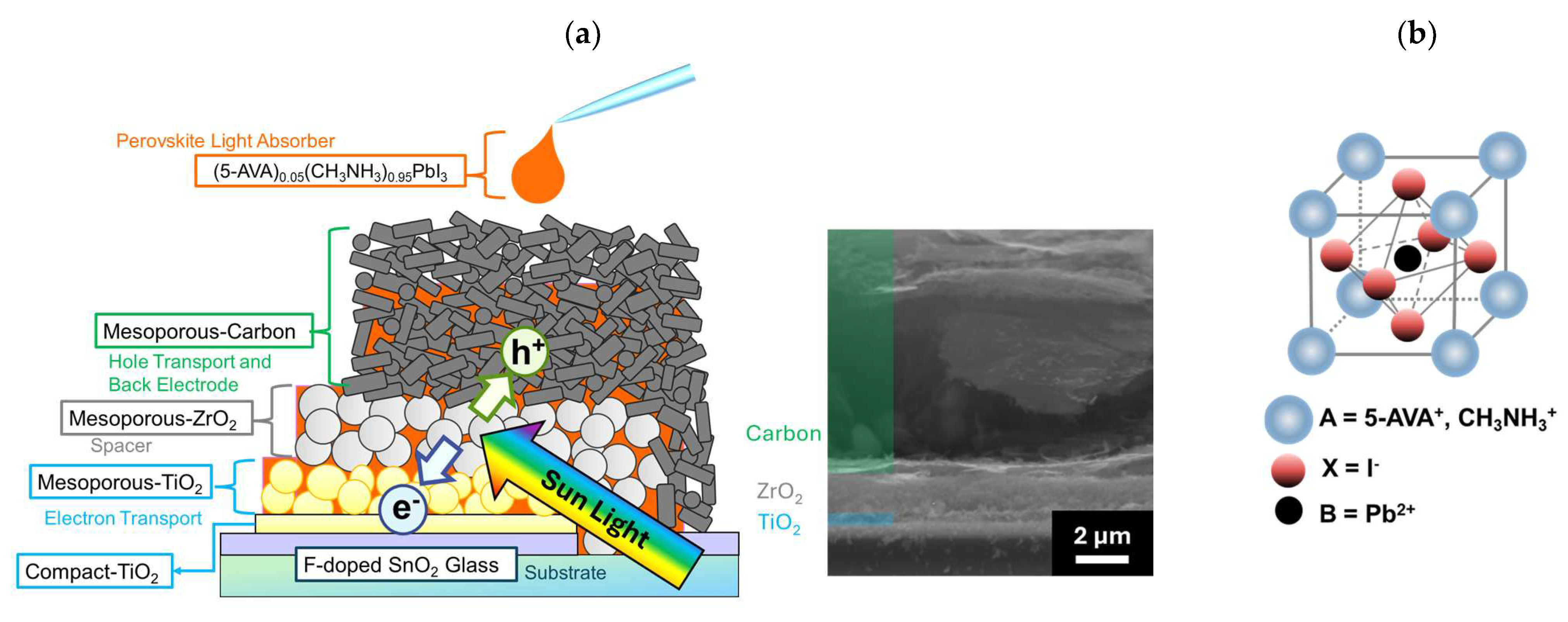
In this study, in order to verify the influence of the morphology (especially pore size) of mesoporous ZrO2 on the corresponding device, we applied five different ZrO2 spacer layers to MPLE−PSCs. These ZrO2 spacer layers were dispersed in paste and deposited via screen printing. MPLE−PSCs composed of <glass/fluorine-doped tin oxide (FTO)/compact TiO2/mesoporous TiO2 + perovskite/mesoporous ZrO2 + perovskite/carbon + perovskite> are shown in Figure 1a. The thickness of these layers was controlled using a screen printing method, and the values were 0.3 to 0.5 μm for mesoporous TiO2, 1.4 to 1.6 μm for mesoporous ZrO2, and 10 to 15 μm for mesoporous carbon, as shown in the scanning electron microscope (SEM) images. MPLE−PSC devices were fabricated in ambient open air via spray pyrolysis deposition and screen printing. 5−AVA−MAPbI3 was used as the light-absorbing material (Figure 1b); this perovskite material has been used since the initial development of MPLE−PSCs, and it provides excellent reproducibility and durability [34,35,36]. However, recent studies have shown that the performance of devices containing perovskite materials, including MAI and 5−AVAI, varies significantly depending on the measurement conditions [63,64]. Therefore, it is important to note that the photoelectric conversion performance shown in this study cannot be replicated in real operating conditions. The morphology of ZrO2 was evaluated using scanning electron microscopy (SEM) and nitrogen adsorption/desorption measurements. The insulation ability of the mesoporous ZrO2 layer between the cathode and anode was evaluated in terms of its electrical resistance before the deposition of the perovskite precursor solution. The light absorbance of MPLE−PSCs was investigated using UV-visible reflection spectra. To investigate the performance of MPLE−PSCs, we performed current density–voltage (J−V) measurements and incident photon-to-current efficiency (IPCE) measurements. Through these measurements, it was confirmed that the specific surface area, pore volume, and size distribution of ZrO2 affected the JSC and open circuit voltage (VOC) of the devices due to the change in light absorption and insulating ability.
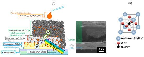
Figure 1.
Schematic images: (a) cross-sectional structure of MPLE−PSCs; (b) 5−AVA−MAPbI3 perovskite light-absorbing crystal.
2. Materials and Methods
2.1. Materials
Lead iodide (PbI2, 99.99%), methylammonium iodide (MAI, 99.0%), 5−ammonium valeric acid iodide (5−AVAI, 97.0%), acetic acid, and ethyl cellulose (45–55 mPa·s) were purchased from Tokyo Chemical Industry Co., Ltd., Tokyo, Japan. γ−butyrolactone (GBL, 99.5%), ethanol (99.5%), and α−terpineol (95.0%) were purchased from Kanto Chemical Co., Inc., Tokyo, Japan. Titanium diisopropoxide bis (acetylacetonate) (TAA, 75 wt.% in isopropanol) was purchased from Sigma-Aldrich, St. Louis, MO, USA. ZrO2 particles (EP, UEP, SRP−2, and SPZ) were obtained from Daiichi Kigenso Kagaku Kogyo Co., Ltd., Osaka, Japan. ZrO2 particles (NP−ZRO2−4−500) were purchased from American Elements, Los Angeles, CA, USA. TiO2 paste and carbon paste were prepared in the laboratory using the same process reported in our previous paper [52,65].
2.2. Preparation of ZrO2 Paste for Mesoporous ZrO2 Layer
A total of 4.5 g of ZrO2 particles, 8.85 g of α–terpineol, 4.05 g of ethyl cellulose dissolved in α–terpineol (10 wt.%), Al2O3 beads (10 mm), and two sizes of ZrO2 beads (5 mm and 2 mm) were placed in an agate pot and crushed and stirred in a planetary ball mill (PULVERISETTE 7, Fritsch Japan Co., Ltd., Yokohama, Japan) for 1 h (700 rpm); then, the paste was milled at a low speed (300 rpm) for 5 min to remove air bubbles.
2.3. Preparation of Perovskite Precursor Solution
The (5−AVA)0.05(CH3NH3)0.95PbI3 precursor solution (1.2 mol L−1 in GBL) was prepared in a glove box filled with nitrogen gas. The precursor solution was prepared by mixing 0.60 mmol of PbI2, 0.57 mmol of MAI, and 0.03 mmol of 5−AVAI in 0.5 mL of GBL. The solution was stirred at 800 rpm for 17.5 h at 70 °C.
2.4. Fabrication of MPLE−PSCs
The perovskite solar cells were fabricated under atmospheric open-air conditions on fluorine-doped tin oxide (FTO)-coated glass substrates (TEC−15, Nippon Sheet Glass Co., Ltd., Tokyo, Japan). We patterned the substrates via laser etching to separate the FTO conductive layers. Then, the patterned substrates were ultrasonically cleaned with detergent solution and ethanol for 15 min each. A compact TiO2 hole-blocking layer was deposited on the patterned FTO glass heated at 500 °C using the spray pyrolysis method. To prepare the precursor solution, 0.66 mL of TAA was diluted with 22.5 mL of ethanol. Then, the mesoporous TiO2 electron transport layer was screen-printed, left to rest at room temperature for 10 min, and after that, dried on a hot plate at 50 °C and 140 °C for 5 min each. The TiO2 layer was annealed at 500 °C for 55 min (25 min rising and 30 min holding) in an electric furnace. The mesoporous ZrO2 spacer layers were similarly screen-printed on the mesoporous TiO2 layer, left to rest at room temperature for 10 min, and after that, they were dried on a hot plate at 50 °C and 140 °C for 5 min each. The ZrO2 layer was annealed on a hot plate at 200 °C for 20 min [66]. Then, the carbon back electrode was screen-printed on the mesoporous ZrO2 spacer, left to rest at room temperature for 10 min, and then it was dried on a hot plate at 125 °C for 10 min. The carbon layer-coated substrate was annealed at 400 °C for 1 h on a hot plate. The substrates were then cooled to room temperature and diced into individual cells, and electrical contacts were attached to both electrodes via ultrasonic soldering. The surrounding area of the multiporous-layered electrodes was masked with heat-resistant polyimide tape so that the perovskite solution would fill the multiporous-layered electrodes. Finally, per cell, 4.0 µL of perovskite precursor solution was drop-casted into the porous electrode layer in the masked area by polyimide tape (the cell and area sizes were 196 and 120 mm2). The solution-dropped devices were left to rest at 25 °C in a Petri dish for 30 min. Then, with the Petri dish covered, they were heated on a hot plate at 50 °C for 90 min. Afterwards, the Petri dish was removed and the devices were dried at 50 °C for 10 min to complete the crystallization of the perovskite material. All perovskite infiltration and crystallization processes were conducted under atmospheric open-air conditions, with room temperature ranging from 15 °C to 25 °C and relative humidity between 20% and 70%.
2.5. Characterization
SEM images of the cross-sectional structure of MPLE−PSCs and mesoporous ZrO2 spacer layers were obtained using a scanning electron microscope (JSM–6510, JEOL, Akishima, Japan) at an accelerating voltage of 10 kV. The specific surface area and pore size distribution were calculated from nitrogen adsorption/desorption isotherm profiles (BELSORP MINI X, MicrotracBEL Corp., Osaka, Japan) using the Brunauer–Emmett–Teller (BET) and the Barrett–Joyner–Halenda (BJH) methods, respectively. UV-visible light reflectance measurements were taken using a UV-visible spectrophotometer (V−650, JASCO, Hachioji, Japan). Current density–voltage (J−V) curves were measured with a DC voltage current source (B2901A, Agilent, CA, USA) under a solar simulator (AM1.5G, 100 mW cm−2) equipped with a 500 W xenon lamp (YSS−100A, Yamashita Electric, Tokyo, Japan). The irradiation intensity of the AM1.5G solar simulator was calibrated using a reference Si photodiode (Bunko Keiki, Tokyo, Japan). The photosensitive area was limited to 0.09 cm2 by masking with 3 mm × 3 mm aperture. The measurement voltage ranged from −0.05 to 1.05 V; forward and reverse scanning were performed; the step was 0.01 V; and the scanning delay time was 10 msec. Measurements were taken three times in the forward direction and three times in the reverse direction, with an interval of 2 min between each measurement. The device was continuously illuminated for photoactivation between measurements [67]. The optical aging under AM1.5G was performed under open-circuit conditions. To take the incident photon-to-current efficiency (IPCE) measurement, a 150 W xenon lamp (Peccell Technologies, Kawasaki, Japan) equipped with a monochromator was used as a light source to obtain the spectrum. Before the measurement, calibration was performed with a Si photodiode.
3. Results and Discussion
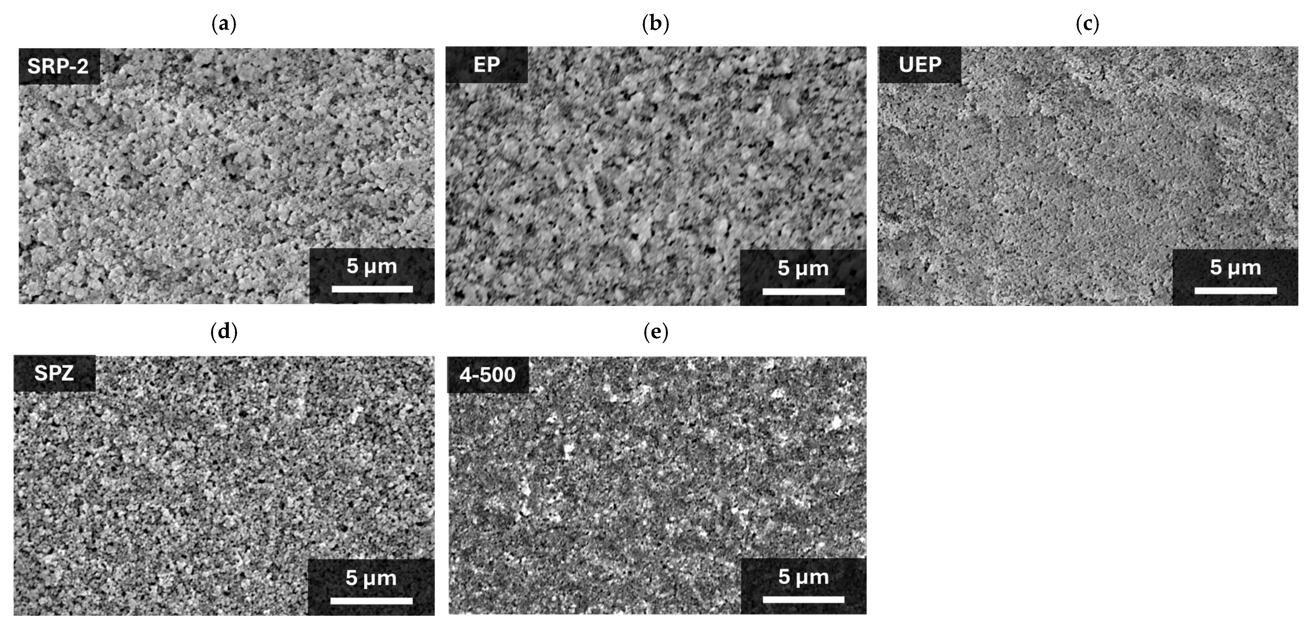
First, to confirm the morphology of ZrO2, five different ZrO2 powders (product−names SRP−2, EP, UEP, SPZ, and NP−ZRO2−4−500 (denoted “4−500”)) were used to prepare the mesoporous ZrO2 spacer layers shown in the SEM images (Figure 2). All of the ZrO2 layers were not removed from the substrate during the processes of printing and annealing, and no cracks were observed. In the SRP−2 and EP layers (Figure 2a,b), large aggregates of about 1 μm were observed. Other ZrO2 (UEP, SPZ, and 4−500) layers (Figure 2c–e) showed no aggregates, and dispersed ZrO2 particles were identified. The particle sizes were 0.1 µm to 0.2 µm for SPZ and less than 0.1 µm for UEP and 4−500.

Figure 2.
Surface SEM images of mesoporous ZrO2 layer: (a) SRP−2; (b) EP; (c) UEP; (d) SPZ; and (e) 4−500.
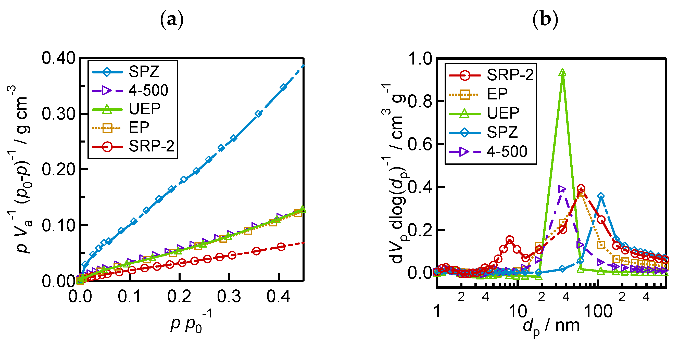
To reveal the pore characteristics of the ZrO2 layers, nitrogen adsorption/desorption measurements were performed to obtain the specific surface area and pore size distribution of ZrO2. The specific surface area of ZrO2 (As), total pore volume (Vp), and medium pore diameter (dp) are shown in Table 1. As was calculated based on the BET plots shown in Figure 3a. Pore size distributions were obtained using the BJH method (Figure 3b). The 4−500 and UEP powders of ZrO2 have pores ranging from 30 to 40 nm. UEP has a higher number of pores than 4−500. SPZ of ZrO2 has the largest number of large pores at around 100 nm. In addition, in the EP and SRP−2 of ZrO2, pores with a wide range of sizes are observed. SRP−2 has pores less than 10 nm, but it is difficult for perovskite precursor solutions to penetrate these small pores [52]. From the above morphology analysis results (Figure 2 and Figure 3), it can be stated that larger ZrO2 particles have larger pore sizes, and the distribution of pore size is influenced by the homogeneity of the particles—in this case, the presence of aggregates is apparent in the SRP−2 and EP layers.

Table 1.
Parameters of the morphology of ZrO2 from nitrogen adsorption/desorption measurements.
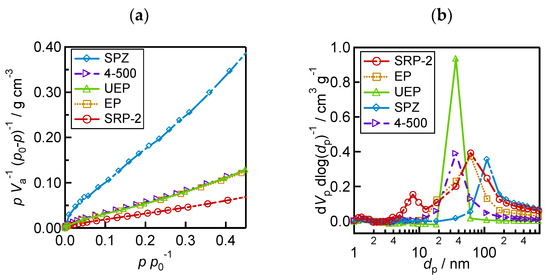
Figure 3.
Analytical results of ZrO2 morphology from nitrogen adsorption/desorption measurements: (a) BET plot for calculating specific surface area; (b) pore size distribution.
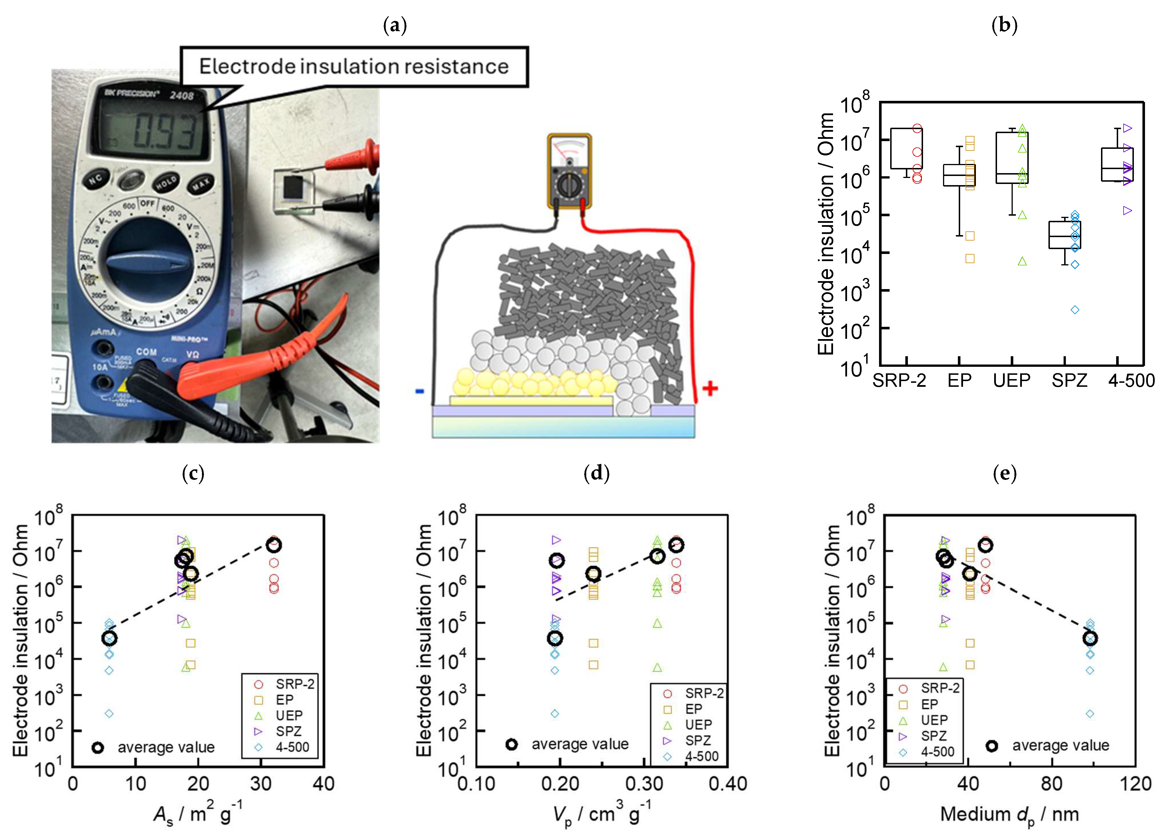
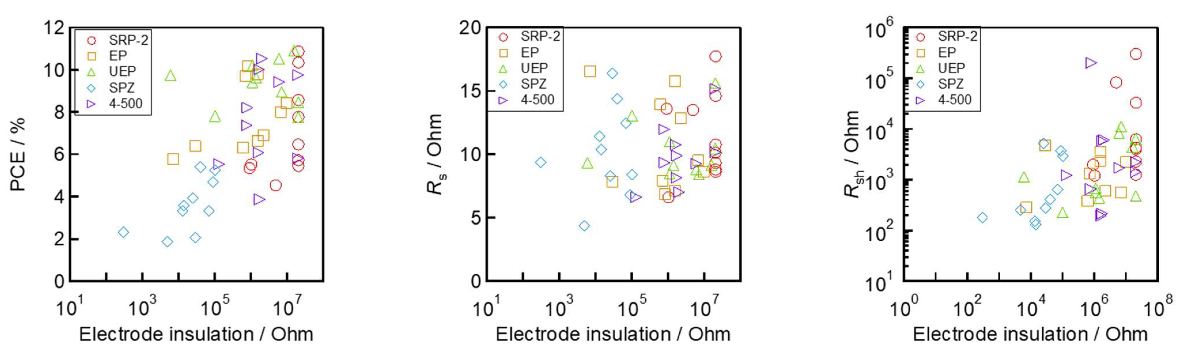
To evaluate the insulation ability of the above mesoporous ZrO2 layers, multiporous layered electrodes composed of <FTO/compact TiO2/mesoporous TiO2/mesoporous ZrO2/mesoporous carbon> were fabricated. The insulation resistance of the electrodes was measured before introducing the perovskite precursor solution, as shown in Figure 4a. The high resistance across the etch line on the FTO glass substrate denotes the prevention of contact between the carbon layer and FTO (or TiO2). The insulation resistance values for each ZrO2 powder are shown in the boxplots in Figure 4b. The measurement apparatus had a maximum resistance limit of 20 MΩ. Hence, when the resistances between the electrodes showed “over range”, we marked the data as “20 MΩ”. In total, 10 cells were used for one type of ZrO2 (50 cells in total). Devices with SPZ had lower insulation resistance compared to the other ZrO2 materials. SRP−2 showed high insulation performance (more than 1 MΩ). Furthermore, we investigated the relationship between ZrO2 morphology and insulation performance. As shown in Figure 4c–e, the morphology parameters obtained from Table 1 are plotted on the x-axis, and the insulation resistance of 10 devices for each ZrO2 and their average values are plotted on the y-axis. The insulation ability increased with the increase in As and Vp and with the decrease in the medium dp. These results indicate that the morphology of ZrO2 affects the insulation ability of the device when applied as a spacer layer.

Figure 4.
Evaluation of the insulation ability of the mesoporous ZrO2 spacer layer: (a) flow of measurement; (b) box and whisker plots (n = 10 cells) of the electrode insulation resistance of each ZrO2; (c) relationship between insulation resistance and As; (d) insulation resistance and Vp; and (e) insulation resistance and medium dp.
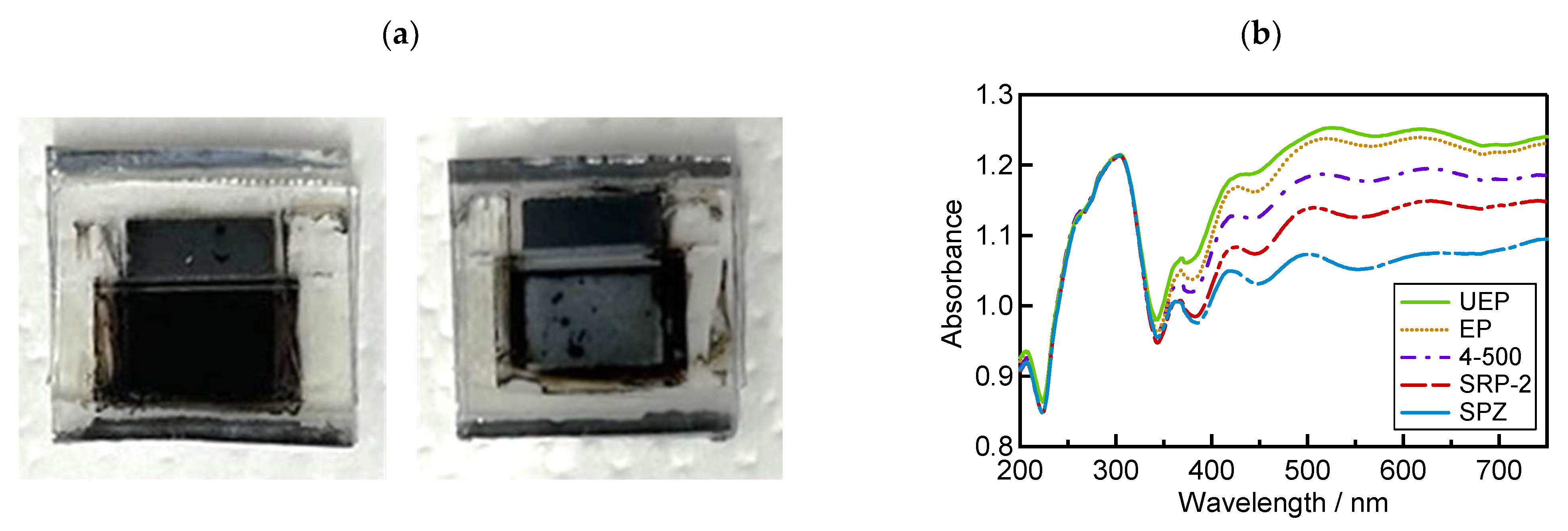
To confirm the light absorbance at the photosensitive area of these devices, UV−vis reflection measurements were performed using the same process as previously reported [52]. The perovskite precursor solution was introduced into the TiO2/ZrO2/carbon scaffold and crystallized via annealing to obtain solar cells. Usually, perovskite crystallization can occur on the whole area in mesoporous electrodes, and the photosensitive area shows a dark black color (Figure 5a, left side). In this case, the value of absorbance will be high, and then a large value for the short-circuit current density (JSC) can be expected. On the contrary, when crystallization does not occur homogeneously, the photosensitive area shows a white or gray color derived from TiO2 and ZrO2 (Figure 5a, right side), and it gains low absorbance. Therefore, it is important to study reflection absorbance to evaluate the crystallization behavior of the perovskite precursor on mesoporous ZrO2 morphologies. Figure 5b shows the reflection absorption spectra of the device using different ZrO2 sources. The results show that the device using UEP achieved the highest absorbance in the visible light range (350 nm to 750 nm).
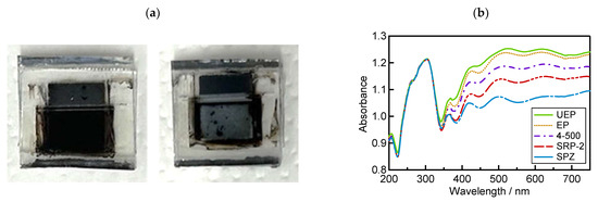
Figure 5.
Investigation results of device absorbance from UV-visible reflectance spectroscopy: (a) photosensitive area of the device; (b) UV-visible absorbance of the device.
To evaluate the photoenergy conversion performance of the fabricated MPLE−PSCs, we obtained the performance parameters, J−V curves, IPCE spectrum, and boxplots prepared based on each parameter, as shown in Table 2 and Table 3 and Figure 6a–d. The hysteresis index (HI) in Table 2 was calculated using Equation (1) as follows:
Table 2.
Best-performing parameters and hysteresis index (HI) of the devices fabricated with different mesoporous ZrO2 layers.
Table 3.
Parameters of the devices fabricated with different mesoporous ZrO2 layers (n = 10 cells).
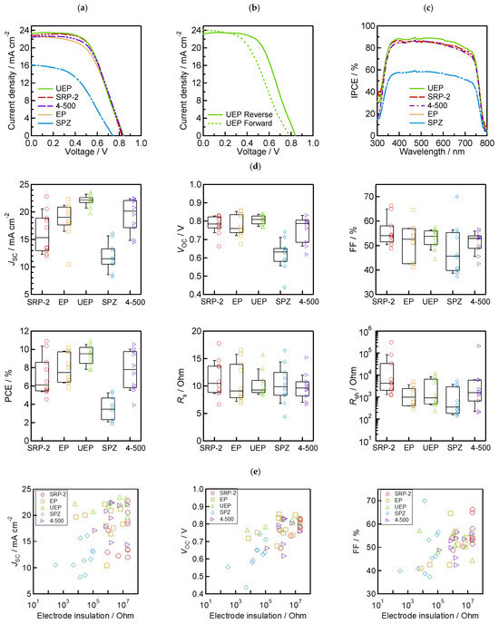
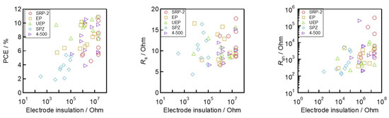
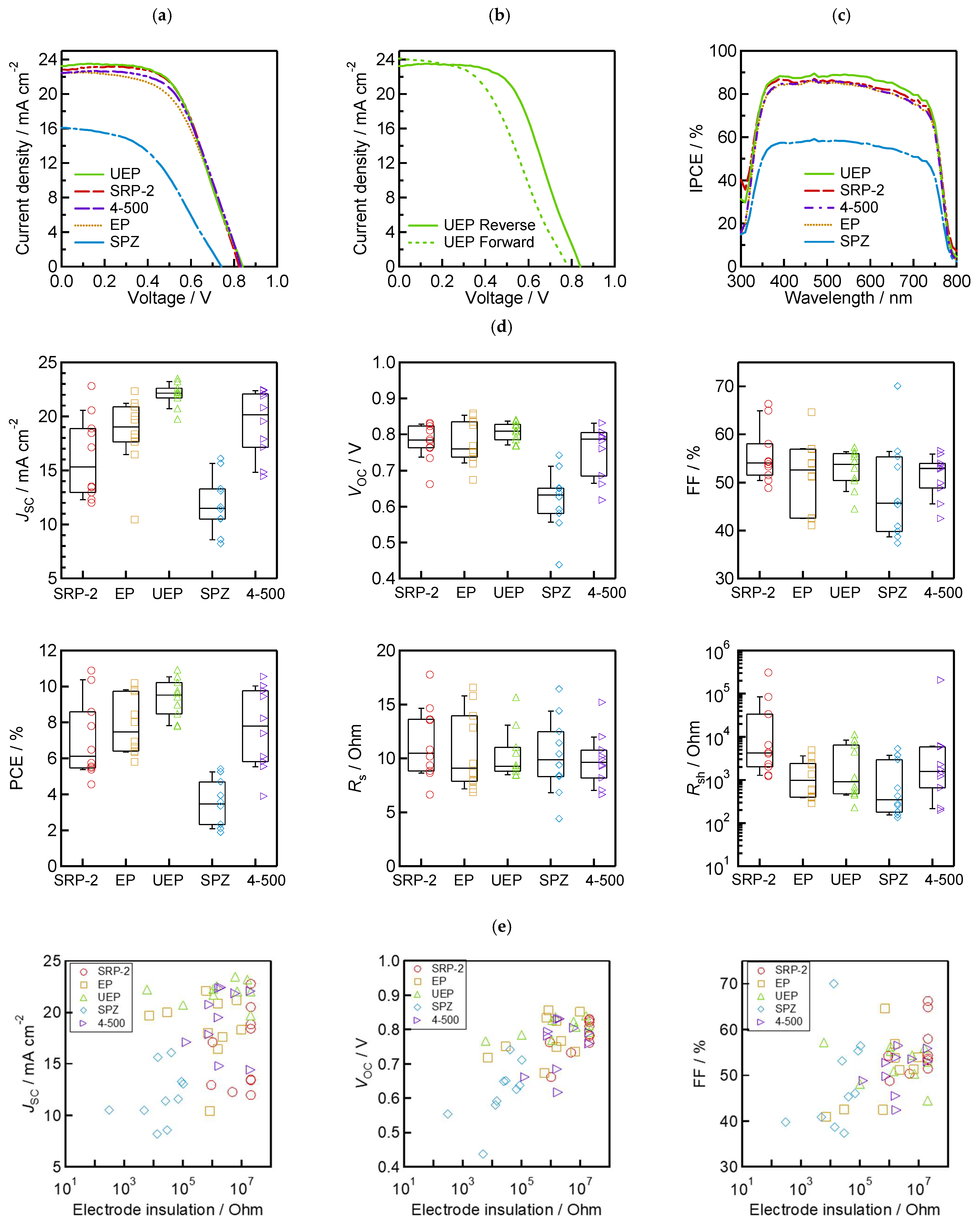
Figure 6.
Device performance: (a) best-performing J−V curves based on five types of ZrO2 spacer layers with different morphologies; (b) forward and reverse scan of UEP’s best-performing J−V curve; (c) IPCE spectrum of best-performing cells; (d) box and whisker plots (n = 10 cells) of each photovoltaic parameter; and (e) the relationship between insulation resistance and each photovoltaic parameter.
The best-performing device achieved 10.92% PCE, 23.22 mA/cm−2 JSC, 0.840 V VOC, and a 56.0% fill factor (FF) on the reverse scan using UEP. Furthermore, the HI was above 10% for all of the best-performing devices. Since a large HI was obtained regardless of the morphology of ZrO2, we assume that this is due to the low quality of the perovskite light-absorbing crystals of 5−AVA−MAPbI3 rather than the result of a problem with ZrO2 [64]. The IPCE values of the best-performing device using UEP exhibited the highest response across the entire visible light region. The other best-performing devices showed similar trends, as reflected in the JSC presented in Table 2 and Figure 6a. These results confirm that the J−V measurements were conducted properly. Comparing the results of these five types of ZrO2 powders, devices using UEP achieved a high performance with good reproducibility. In particular, JSC increased with the increase in the absorbance value of the device in the visible light region, and reproducibility improved. In contrast, lower absorbance values result in lower JSC.
The relationships between the electrodes’ insulation resistance and solar cell performance are shown in Figure 6e. The results show linear relationships of PCE, VOC, FF, and shunt resistance (Rsh) in terms of electrode insulation resistance. In particular, a strong relationship between VOC and electrode insulation resistance was identified, and this trend is consistent with the findings of a previous study [54]. The series resistance (Rs) with low values (below 10 Ω) in the devices was also commonly observed when the electrode insulation resistance was high. This may be because proper interfacial contact is achieved due to the good separation of the carrier transport layer (TiO2 and carbon) using the ZrO2 spacer. The correlation of JSC and electrode insulation resistance cannot be confirmed because JSC is a parameter attributed to light absorption. As expected from these results, the high PCE, resulting in the increase in VOC and FF, with high electrode insulation resistance, is due to the increase in Rsh associated with the suppression of non-radiative recombination in the device.
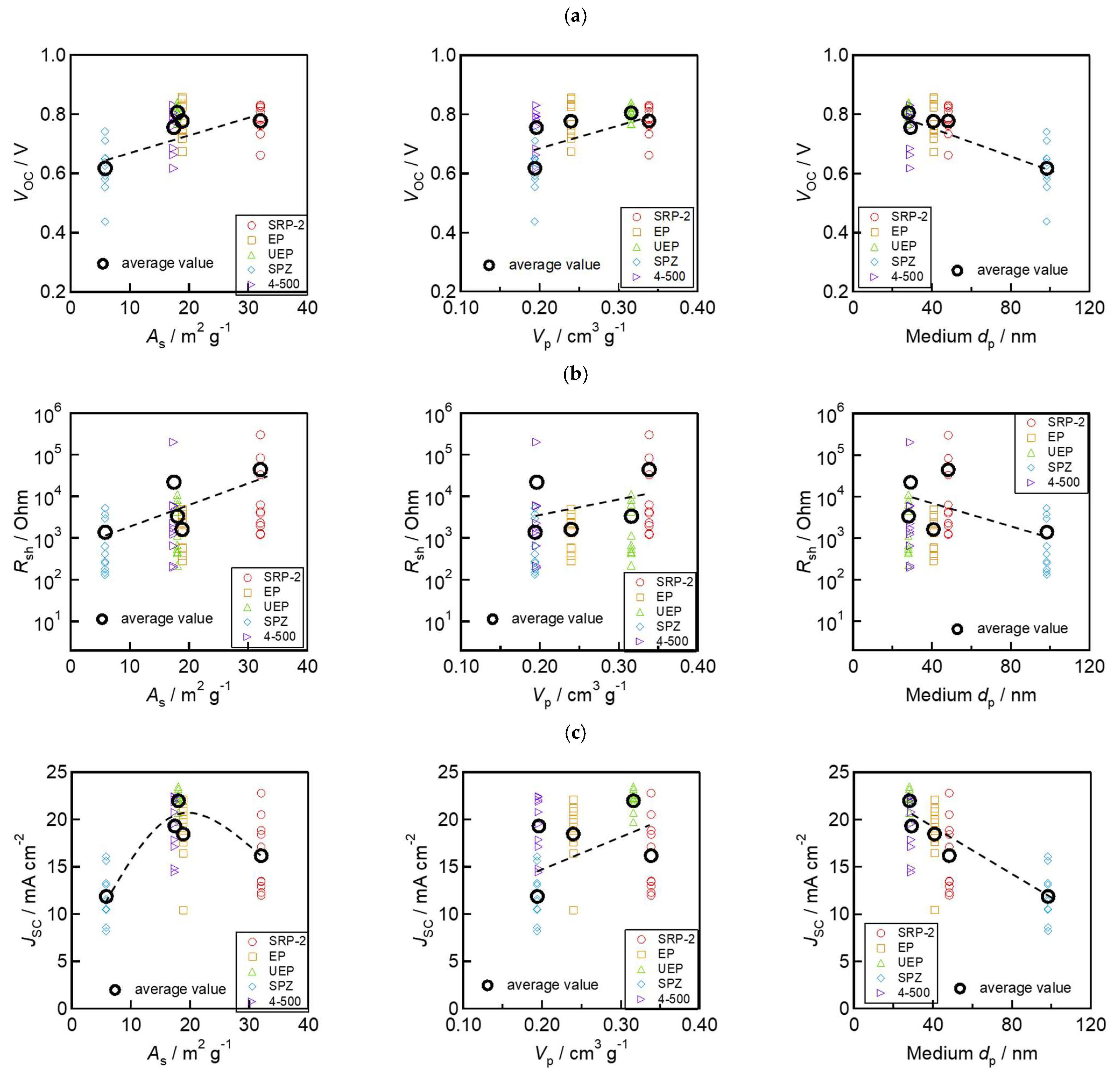
Next, the relationships between ZrO2 morphology parameters (As, Vp, and medium dp) and device performances (VOC, Rsh, and JSC) are shown in Figure 7. The values of VOC and Rsh increased with the increase in As and Vp and with the decrease in the medium dp (Figure 7a,b). This trend is consistent with the trend for the electrodes’ insulation resistance outlined in Figure 4c–e. These results indicate that the good separation of the charge transport layers using the ZrO2 spacer layer can reduce VOC loss by suppressing the risk of electron and hole recombination. Moreover, it is also interesting to note that JSC shows the different variation in trends from Rsh to VOC (Figure 7c). This indicates that controlling the morphology of ZrO2 can work not only to improve the insulating capacity, but also to assist with the formation of light-absorbing perovskite crystal in solar cells. SRP−2, which has large As and Vp, has smaller JSC and absorbance in the devices. This is likely due to the small (<10 nm) pores contained in SRP−2, which prevent the permeation of perovskite precursor solution and the lower filling rate of light-absorbing crystals. These results can be linked to the findings reported in a previous study [55,56]. Specifically, a small pore size in the ZrO2 layer can hinder the complete filling of the perovskite light-absorbing crystals throughout the mesoporous electrode. In such cases, the device’s light absorbance may become limited. To make further improvements to achieve high-efficiency devices, it is necessary to carefully control the morphology and thickness of the ZrO2 and other mesoporous layers. In addition, optimizing the infiltration conditions and the crystallization process of the perovskite material is essential.
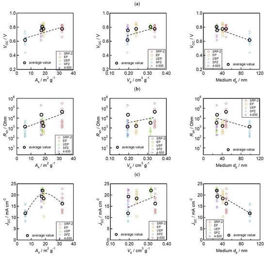
Figure 7.
Relationship between morphology of ZrO2 and photovoltaic parameters: (a) VOC and morphology; (b) Rsh and morphology; and (c) JSC and morphology.
4. Conclusions
We investigated the effect of the morphology of the mesoporous ZrO2 layer on insulation ability and device performance by making a comparison with five different types of ZrO2. This study outlines how to achieve good separation between TiO2 and carbon and devices with high absorbance and high efficiency via optimizing the morphological properties of the ZrO2 spacer layer. In conclusion, as shown in Figure 8, mesoporous ZrO2 layers should be designed based on the following characteristics to obtain high-efficiency devices:
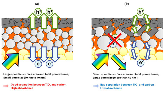
Figure 8.
Illustration of two types of mesoporous ZrO2 spacer layers: (a) smooth carrier transport and high light absorption due to ideal morphology; (b) complicated carrier transport and non-radiative recombination and reflection of visible light due to poor morphology.
Future morphological research on spacer materials should place particular emphasis on controlling the crystallization behavior of the perovskite light absorber, aiming to achieve further enhancements in light harvesting efficiency and overall device performance. In addition, evaluating the morphological uniformity of the mesoporous layer when the device is scaled up may represent a critical factor in the commercial potential of MPLE−PSCs. These results will be helpful for designing the material morphology of MPLE−PSCs using ZrO2 spacers and other mesoporous carrier transport layers, or other devices, using porous materials.
Author Contributions
Investigation, N.I.; methodology, T.S. and R.T.; resources, F.I.; supervision, F.I. and S.I.; visualization, T.S. and N.I.; writing—original draft, T.S.; writing—review and editing, R.T. and S.I. All authors have read and agreed to the published version of the manuscript.
Funding
This research received no external funding.
Data Availability Statement
The original contributions presented in this study are included in the article. Further inquiries can be directed to the corresponding author.
Conflicts of Interest
The author, Fumitaka Iwakura, is employed by the company Daiichi Kigenso Kagaku Kogyo Co., Ltd.
Abbreviations
The following abbreviations are used in this manuscript:
| PSCs | Perovskite solar cells |
| MPLE−PSCs | Multiporous layered electrode perovskite solar cells |
| FTO | Fluorine-doped tin oxide |
| SEM | Scanning electron microscope |
| BET | Brunauer–Emmett–Teller |
| BJH | Barrett–Joyner–Halenda |
| As | Specific surface area |
| Vp | Total pore volume |
| Medium dp | Medium pore diameter |
| PCE | Photoelectric conversion efficiency |
| JSC | Short-circuit current density |
| VOC | Open circuit voltage |
| FF | Fill factor |
| Rs | Series resistance |
| Rsh | Shunt resistance |
References
- Kojima, A.; Teshima, K.; Shirai, Y.; Miyasaka, T. Organometal Halide Perovskites as Visible-Light Sensitizers for Photovoltaic Cells. J. Am. Chem. Soc. 2009, 131, 6050–6051. [Google Scholar] [CrossRef] [PubMed]
- Arora, N.; Dar, M.I.; Abdi-Jalebi, M.; Giordano, F.; Pellet, N.; Jacopin, G.; Friend, R.H.; Zakeeruddin, S.M.; Grätzel, M. Intrinsic and Extrinsic Stability of Formamidinium Lead Bromide Perovskite Solar Cells Yielding High Photovoltage. Nano Lett. 2016, 16, 7155–7162. [Google Scholar] [CrossRef] [PubMed]
- Xiao, X.; Zhang, W.; Zhang, W.; Du, J.; Zhang, C.; Xu, G.; Mei, A.; Rong, Y.; Hu, Y.; Han, H. Cl-Assisted Perovskite Crystallization Pathway in the Confined Space of Mesoporous Metal Oxides Unveiled by in Situ Grazing Incidence Wide-Angle X-Ray Scattering. Chem. Mater. 2022, 34, 2231–2237. [Google Scholar] [CrossRef]
- Nakamura, T.; Yakumaru, S.; Truong, M.A.; Kim, K.; Liu, J.; Hu, S.; Otsuka, K.; Hashimoto, R.; Murdey, R.; Sasamori, T.; et al. Sn(IV)-free tin perovskite films realized by in situ Sn(0) nanoparticle treatment of the precursor solution. Nat. Commun. 2020, 11, 3008. [Google Scholar] [CrossRef] [PubMed]
- Ito, N.; Kamarudin, M.A.; Hirotani, D.; Zhang, Y.; Shen, Q.; Ogomi, Y.; Iikubo, S.; Minemoto, T.; Yoshino, K.; Hayase, S. Mixed Sn-Ge Perovskite for Enhanced Perovskite Solar Cell Performance in Air. J. Phys. Chem. Lett. 2018, 9, 1682–1688. [Google Scholar] [CrossRef] [PubMed]
- Jong, U.G.; Yu, C.J.; Kim, Y.S.; Kye, Y.H.; Kim, C.H. First-principles study on the material properties of the inorganic perovskite Rb1-XCsxPbI3 for solar cell applications. Phys. Rev. B 2018, 98, 125116. [Google Scholar] [CrossRef]
- Nam, J.K.; Chai, S.U.; Cha, W.; Choi, Y.J.; Kim, W.; Jung, M.S.; Kwon, J.; Kim, D.; Park, J.H. Potassium Incorporation for Enhanced Performance and Stability of Fully Inorganic Cesium Lead Halide Perovskite Solar Cells. Nano Lett. 2017, 17, 2028–2033. [Google Scholar] [CrossRef] [PubMed]
- Sun, H.; Zhang, J.; Gan, X.; Yu, L.; Yuan, H.; Shang, M.; Lu, C.; Hou, D.; Hu, Z.; Zhu, Y.; et al. Pb-Reduced CsPb0.9Zn0.1I2Br Thin Films for Efficient Perovskite Solar Cells. Adv. Energy Mater. 2019, 9, 1900896. [Google Scholar] [CrossRef]
- Bi, D.; Tress, W.; Dar, M.I.; Gao, P.; Luo, J.; Renevier, C.; Schenk, K.; Abate, A.; Giordano, F.; Correa Baena, J.P.; et al. Efficient luminescent solar cells based on tailored mixed-cation perovskites. Sci. Adv. 2016, 2, e1501170. [Google Scholar] [CrossRef] [PubMed]
- Jeon, N.J.; Noh, J.H.; Kim, Y.C.; Yang, W.S.; Ryu, S.; Seok, S. Il Solvent engineering for high-performance inorganic-organic hybrid perovskite solar cells. Nat. Mater. 2014, 13, 897–903. [Google Scholar] [CrossRef] [PubMed]
- Jeon, N.J.; Noh, J.H.; Yang, W.S.; Kim, Y.C.; Ryu, S.; Seo, J.; Seok, S., II. Compositional engineering of perovskite materials for high-performance solar cells. Nature 2015, 517, 476–480. [Google Scholar] [CrossRef] [PubMed]
- Lapotre, M.G.A.; Ewing, R.C.; Lamb, M.P.; Fischer, W.W.; Grotzinger, J.P.; Rubin, D.M.; Lewis, K.W.; Ballard, M.J.; Day, M.; Gupta, S.; et al. Large wind ripples on Mars: A record of atmospheric evolution. Science 2016, 353, 55–58. [Google Scholar] [CrossRef] [PubMed]
- Etgar, L.; Gao, P.; Xue, Z.; Peng, Q.; Chandiran, A.K.; Liu, B.; Nazeeruddin, M.K.; Grätzel, M. Mesoscopic CH3NH3PbI3/TiO2 Heterojunction Solar Cells. J. Am. Chem. Soc. 2012, 134, 17396–17399. [Google Scholar] [CrossRef] [PubMed]
- NREL Best Research-Cell PV Efficiency Chart. Available online: https://www.nrel.gov/pv/cell-efficiency.html (accessed on 17 February 2025).
- Lee, M.M.; Teuscher, J.; Miyasaka, T.; Murakami, T.N.; Snaith, H.J. Efficient Hybrid Solar Cells Based on Meso-Superstructured Organometal Halide Perovskites. Science 2012, 338, 643–647. [Google Scholar] [CrossRef] [PubMed]
- Liu, M.; Johnston, M.B.; Snaith, H.J. Efficient planar heterojunction perovskite solar cells by vapour deposition. Nature 2013, 501, 395–398. [Google Scholar] [CrossRef] [PubMed]
- Burschka, J.; Pellet, N.; Moon, S.J.; Humphry-Baker, R.; Gao, P.; Nazeeruddin, M.K.; Grätzel, M. Sequential deposition as a route to high-performance perovskite-sensitized solar cells. Nature 2013, 499, 316–319. [Google Scholar] [CrossRef] [PubMed]
- Heo, J.H.; Im, S.H.; Noh, J.H.; Mandal, T.N.; Lim, C.S.; Chang, J.A.; Lee, Y.H.; Kim, H.J.; Sarkar, A.; Nazeeruddin, M.K.; et al. Efficient inorganic-organic hybrid heterojunction solar cells containing perovskite compound and polymeric hole conductors. Nat. Photonics 2013, 7, 486–491. [Google Scholar] [CrossRef]
- Xing, G.; Mathews, N.; Sun, S.; Lim, S.S.; Lam, Y.M.; Grätzel, M.; Mhaisalkar, S.; Sum, T.C. Long-Range Balanced Electron- and Hole-Transport Lengths in Organic-Inorganic CH3NH3PbI3. Science 2013, 342, 344–347. [Google Scholar] [CrossRef] [PubMed]
- Noh, J.H.; Im, S.H.; Heo, J.H.; Mandal, T.N.; Seok, S., II. Chemical Management for Colorful, Efficient, and Stable Inorganic-Organic Hybrid Nanostructured Solar Cells. Nano Lett. 2013, 13, 1764–1769. [Google Scholar] [CrossRef] [PubMed]
- Eperon, G.E.; Stranks, S.D.; Menelaou, C.; Johnston, M.B.; Herz, L.M.; Snaith, H.J. Formamidinium lead trihalide: A broadly tunable perovskite for efficient planar heterojunction solar cells. Energy Environ. Sci. 2014, 7, 982–988. [Google Scholar] [CrossRef]
- Pang, S.; Hu, H.; Zhang, J.; Lv, S.; Yu, Y.; Wei, F.; Qin, T.; Xu, H.; Liu, Z.; Cui, G. NH2CH=NH2PbI3: An Alternative Organolead Iodide Perovskite Sensitizer for Mesoscopic Solar Cells. Chem. Mater. 2014, 26, 1485–1491. [Google Scholar] [CrossRef]
- Rong, Y.; Liu, L.; Mei, A.; Li, X.; Han, H. Beyond Efficiency: The Challenge of Stability in Mesoscopic Perovskite Solar Cells. Adv. Energy Mater. 2015, 5, 1501066. [Google Scholar] [CrossRef]
- Wang, Z.; Shi, Z.; Li, T.; Chen, Y.; Huang, W. Stability of Perovskite Solar Cells: A Prospective on the Substitution of the A Cation and X Anion. Angew. Chem. Int. Ed. 2017, 56, 1190–1212. [Google Scholar] [CrossRef] [PubMed]
- Ku, Z.; Rong, Y.; Xu, M.; Liu, T.; Han, H. Full Printable Processed Mesoscopic CH3NH3PbI3/TiO2 Heterojunction Solar Cells with Carbon Counter Electrode. Sci. Rep. 2013, 3, 3132. [Google Scholar] [CrossRef] [PubMed]
- Wu, W.Q.; Wang, Q.; Fang, Y.; Shao, Y.; Tang, S.; Deng, Y.; Lu, H.; Liu, Y.; Li, T.; Yang, Z.; et al. Molecular doping enabled scalable blading of efficient hole-transport-layer-free perovskite solar cells. Nat. Commun. 2018, 9, 1625. [Google Scholar] [CrossRef] [PubMed]
- Hwang, K.; Jung, Y.S.; Heo, Y.J.; Scholes, F.H.; Watkins, S.E.; Subbiah, J.; Jones, D.J.; Kim, D.Y.; Vak, D. Toward large scale roll-to-roll production of fully printed perovskite solar cells. Adv. Mater. 2015, 27, 1241–1247. [Google Scholar] [CrossRef] [PubMed]
- Worsley, C.; Potts, S.J.; Hughes, D.; Tsoi, W.C.; Watson, T. Age-Induced Excellence with Green Solvents: The Impact of Residual Solvent and Post-Treatments in Screen-Printed Carbon Perovskite Solar Cells and Modules. Mater. Adv. 2024, 5, 4354–4365. [Google Scholar] [CrossRef]
- Liu, S.; Li, J.; Xiao, W.; Chen, R.; Sun, Z.; Zhang, Y.; Lei, X.; Hu, S.; Kober-Czerny, M.; Wang, J.; et al. Buried Interface Molecular Hybrid for Inverted Perovskite Solar Cells. Nature 2024, 632, 536–542. [Google Scholar] [CrossRef] [PubMed]
- Li, S.; Jiang, Y.; Xu, J.; Wang, D.; Ding, Z.; Zhu, T.; Chen, B.; Yang, Y.; Wei, M.; Guo, R.; et al. High-Efficiency and Thermally Stable FACsPbI3 Perovskite Photovoltaics. Nature 2024, 635, 82–88. [Google Scholar] [CrossRef] [PubMed]
- Thangavel, N.R.; Koh, T.M.; Chee, Z.Q.; Tay, D.J.J.; Lee, M.J.; Mhaisalkar, S.G.; Ager, J.W.; Mathews, N. Printable Low-Temperature Carbon for Highly Efficient and Stable Mesoscopic Perovskite Solar Cells. Energy Technol. 2022, 10, 2200559. [Google Scholar] [CrossRef]
- Park, S.J.; Eng, J.L.; Pethe, S.D.; Tay, D.J.J.; Yantara, N.; Mathews, N. Investigating the Effects of a High Boiling Point Solvent in Slot Die-Coated Halide Perovskite Solar Cells. ChemSusChem 2025, 18, e202402499. [Google Scholar] [CrossRef] [PubMed]
- Rana, P.J.S.; Febriansyah, B.; Koh, T.M.; Muhammad, B.T.; Salim, T.; Hooper, T.J.N.; Kanwat, A.; Ghosh, B.; Kajal, P.; Lew, J.H.; et al. Alkali Additives Enable Efficient Large Area (>55 cm2) Slot-Die Coated Perovskite Solar Modules. Adv. Funct. Mater. 2022, 32, 2113026. [Google Scholar] [CrossRef]
- Mei, A.; Li, X.; Liu, L.; Ku, Z.; Liu, T.; Rong, Y.; Xu, M.; Hu, M.; Chen, J.; Yang, Y.; et al. A hole-conductor–free, fully printable mesoscopic perovskite solar cell with high stability. Science 2014, 345, 295–298. [Google Scholar] [CrossRef] [PubMed]
- Kobayashi, E.; Tsuji, R.; Martineau, D.; Hinsch, A.; Ito, S. Light-induced performance increase of carbon-based perovskite solar module for 20-year stability. Cell Rep. Phys. Sci. 2021, 2, 100648. [Google Scholar] [CrossRef]
- Grancini, G.; Roldán-Carmona, C.; Zimmermann, I.; Mosconi, E.; Lee, X.; Martineau, D.; Narbey, S.; Oswald, F.; De Angelis, F.; Graetzel, M.; et al. One-Year stable perovskite solar cells by 2D/3D interface engineering. Nat. Commun. 2017, 8, 15684. [Google Scholar] [CrossRef] [PubMed]
- Baranwal, A.K.; Kanda, H.; Shibayama, N.; Masutani, H.; Peiris, T.A.N.; Kanaya, S.; Segawa, H.; Miyasaka, T.; Ito, S. Thermal Degradation Analysis of Sealed Perovskite Solar Cell with Porous Carbon Electrode at 100 °C for 7000 h. Energy Technol. 2019, 7, 245–252. [Google Scholar] [CrossRef]
- Liu, J.; Chen, X.; Chen, K.; Tian, W.; Sheng, Y.; Jiang, Y.; Zhang, D.; Liu, Y.; Qi, J.; Chen, K.; et al. Electron injection and defect passivation for high-efficiency mesoporous perovskite solar cells. Science 2024, 383, 1198–1204. [Google Scholar] [CrossRef] [PubMed]
- Wang, D.; Zhang, Z.; Huang, T.; She, B.; Liu, B.; Chen, Y.; Wang, L.; Wu, C.; Xiong, J.; Huang, Y.; et al. Crystallization Kinetics Control Enabled by a Green Ionic Liquid Additive toward Efficient and Stable Carbon-Based Mesoscopic Perovskite Solar Cells. ACS Appl. Mater. Interfaces 2022, 14, 9161–9171. [Google Scholar] [CrossRef] [PubMed]
- Srisamran, N.; Sudchanham, J.; Sriprachuabwong, C.; Srisawad, K.; Pakawatpanurut, P.; Lohawet, K.; Kumnorkaew, P.; Krajangsang, T.; Tuantranont, A. Enhanced Performance and Stability of Fully Printed Perovskite Solar Cells and Modules by Ternary Additives under High Humidity. Energy Fuels 2023, 37, 6049–6061. [Google Scholar] [CrossRef]
- Tao, Y.; Chen, Y.; Shao, W.; Zhu, W.; Guo, R.; Zhang, Z.; Huang, Y.; Xiong, J.; Xiang, D.; Wang, D.; et al. Natural molecule niacin enables printable carbon-based mesoscopic perovskite solar cells with 17.3% efficiency. J. Mater. Sci. Mater. Electron. 2024, 35, 930. [Google Scholar] [CrossRef]
- Keremane, K.S.; Prathapani, S.; Haur, L.J.; Bruno, A.; Priyadarshi, A.; Adhikari, A.V.; Mhaisalkar, S.G. Improving the Performance of Carbon-Based Perovskite Solar Modules (70 cm2) by Incorporating Cesium Halide in Mesoporous TiO2. ACS Appl. Energy Mater. 2021, 4, 249–258. [Google Scholar] [CrossRef]
- Cheng, Y.; Xiang, J.; Li, X.; Zhang, G.; Xia, M.; Han, C.; Zheng, Z.; Chen, L.; Chen, K.; Ma, Y.; et al. Wettability Sequence Optimization and Interface Strain Buffering in Triple Mesoporous Layer-Based Printable Perovskite Solar Cells for Enhanced Performance. Adv. Mater. 2025, 37, 2413151. [Google Scholar] [CrossRef] [PubMed]
- Qiu, Z.; Liu, J.; Han, C.; Wang, C.; Xiang, J.; Zheng, Z.; Xia, M.; Zhou, Y.; Mei, A.; Han, H. Decylammonium Sulfate Post-Treatment for Efficient Hole-Conductor-Free Printable Perovskite Solar Cells with Reduced Voltage Loss. Commun. Mater. 2024, 5, 221. [Google Scholar] [CrossRef]
- Xiang, J.; Cheng, Y.; Zhang, G.; Liu, Z.; Han, C.; Gao, Q.; Wang, C.; Xie, J.; Li, S.; Zhou, Z.; et al. Efficient Carbon-Based Hole-Conductor-Free Printable Mesoscopic Perovskite Solar Cells via a Multifunctional Fluorinated Molecule. Adv. Funct. Mater. 2024, 34, 2402816. [Google Scholar] [CrossRef]
- Liu, S.; Zhang, D.; Sheng, Y.; Zhang, W.; Qin, Z.; Qin, M.; Li, S.; Wang, Y.; Gao, C.; Wang, Q.; et al. Highly oriented MAPbI3 crystals for efficient hole-conductor-free printable mesoscopic perovskite solar cells. Fundam. Res. 2022, 2, 276–283. [Google Scholar] [CrossRef] [PubMed]
- Ko, S.G.; Ryu, G., II; Kim, B.; Cha, G.J.; Ri, J.H.; Sonu, G.S.; Kim, U.C. Effects of Thiourea on the Perovskite Crystallization for Fully Printable Solar Cells. Sol. Energy Mater. Sol. Cells 2019, 196, 105–110. [Google Scholar] [CrossRef]
- Hashmi, S.G.; Martineau, D.; Li, X.; Ozkan, M.; Tiihonen, A.; Dar, M.I.; Sarikka, T.; Zakeeruddin, S.M.; Paltakari, J.; Lund, P.D.; et al. Air Processed Inkjet Infiltrated Carbon Based Printed Perovskite Solar Cells with High Stability and Reproducibility. Adv. Mater. Technol. 2017, 2, 1600183. [Google Scholar] [CrossRef]
- Meroni, S.; Mouhamad, Y.; De Rossi, F.; Pockett, A.; Baker, J.; Escalante, R.; Searle, J.; Carnie, M.; Jewell, E.; Oskam, G.; et al. Homogeneous and Highly Controlled Deposition of Low Viscosity Inks and Application on Fully Printable Perovskite Solar Cells. Sci. Technol. Adv. Mater. 2018, 19, 1–9. [Google Scholar] [CrossRef]
- Tsuji, R.; Bogachuk, D.; Martineau, D.; Wagner, L.; Kobayashi, E.; Funayama, R.; Matsuo, Y.; Mastroianni, S.; Hinsch, A.; Ito, S. Function of Porous Carbon Electrode during the Fabrication of Multiporous-Layered-Electrode Perovskite Solar Cells. Photonics 2020, 7, 133. [Google Scholar] [CrossRef]
- Tsuji, R.; Tanaka, K.; Oishi, K.; Shioki, T.; Satone, H.; Ito, S. Role and Function of Polymer Binder Thickeners in Carbon Pastes for Multiporous-Layered-Electrode Perovskite Solar Cells. Chem. Mater. 2023, 35, 8574–8589. [Google Scholar] [CrossRef]
- Shioki, T.; Tsuji, R.; Oishi, K.; Fukumuro, N.; Ito, S. Designed Mesoporous Architecture by 10–100 nm TiO2 as Electron Transport Materials in Carbon-Based Multiporous-Layered-Electrode Perovskite Solar Cells. Photonics 2024, 11, 236. [Google Scholar] [CrossRef]
- Hu, Y.; Si, S.; Mei, A.; Rong, Y.; Liu, H.; Li, X.; Han, H. Stable Large-Area (10 × 10 cm2) Printable Mesoscopic Perovskite Module Exceeding 10% Efficiency. Solar RRL 2017, 1, 1600019. [Google Scholar] [CrossRef]
- Liu, T.; Xiong, Y.; Mei, A.; Hu, Y.; Rong, Y.; Xu, M.; Wang, Z.; Lou, L.; Du, D.; Zheng, S.; et al. Spacer layer design for efficient fully printable mesoscopic perovskite solar cells. RSC Adv. 2019, 9, 29840–29846. [Google Scholar] [CrossRef] [PubMed]
- Wang, Q.; Liu, S.; Ming, Y.; Guan, Y.; Li, D.; Zhang, C.; Wang, Z.; Rong, Y.; Hu, Y.; Han, H. Improvements in printable mesoscopic perovskite solar cells: Via thinner spacer layers. Sustain. Energy Fuels 2018, 2, 2412–2418. [Google Scholar] [CrossRef]
- Liu, T.; Liu, L.; Hu, M.; Yang, Y.; Zhang, L.; Mei, A.; Han, H. Critical parameters in TiO2/ZrO2/Carbon-based mesoscopic perovskite solar cell. J. Power Sources 2015, 293, 533–538. [Google Scholar] [CrossRef]
- Cao, K.; Zuo, Z.; Cui, J.; Shen, Y.; Moehl, T.; Zakeeruddin, S.M.; Grätzel, M.; Wang, M. Efficient screen printed perovskite solar cells based on mesoscopic TiO2/Al2O3/NiO/carbon architecture. Nano Energy 2015, 17, 171–179. [Google Scholar] [CrossRef]
- Liu, S.; Cao, K.; Li, H.; Song, J.; Han, J.; Shen, Y.; Wang, M. Full printable perovskite solar cells based on mesoscopic TiO2/Al2O3/NiO (carbon nanotubes) architecture. Solar Energy 2017, 144, 158–165. [Google Scholar] [CrossRef]
- Meng, Z.; Guo, D.; Yu, J.; Fan, K. Investigation of Al2O3 and ZrO2 spacer layers for fully printable and hole-conductor-free mesoscopic perovskite solar cells. Appl. Surf. Sci. 2018, 430, 632–638. [Google Scholar] [CrossRef]
- Cheng, N.; Liu, P.; Bai, S.; Yu, Z.; Liu, W.; Guo, S.S.; Zhao, X.Z. Application of mesoporous SiO2 layer as an insulating layer in high performance hole transport material free CH3NH3PbI3 perovskite solar cells. J. Power Sources 2016, 321, 71–75. [Google Scholar] [CrossRef]
- Liu, H.; Yang, B.; Chen, H.; Li, K.; Liu, G.; Yuan, Y.; Gao, Y.; Zhou, C. Efficient and stable hole-conductor-free mesoscopic perovskite solar cells using SiO2 as blocking layer. Org. Electron. 2018, 58, 69–74. [Google Scholar] [CrossRef]
- Bhandari, S.; Valsalakumar, S.; Ali, M.S.; Mallick, T.K.; Hinshelwood, J.; Sundaram, S. Influence of Adjustable CeO2 Morphology on the Performance of Ambient Hole Transport Layer-Free Carbon-Based Perovskite Solar Cells. Energy Fuels 2025, 39, 9566–9575. [Google Scholar] [CrossRef] [PubMed]
- Perrin, L.; Planes, E.; Shioki, T.; Tsuji, R.; Honore, J.C.; Farha, C.; Ito, S.; Flandin, L. How Ammonium Valeric Acid Iodide Additive Can Lead to More Efficient and Stable Carbon-Based Perovskite Solar Cells: Role of Microstructure and Interfaces? Solar RRL 2024, 8, 2400393. [Google Scholar] [CrossRef]
- Tsuji, R.; Shioki, T.; Izumoto, N.; Oshita, S.; Kondo, T.; Ito, S. Hysteresis in Carbon-Based Multiporous Layered Electrode Perovskite Solar Cells with 5-AVA-MAPbI3 and CsFAPbI3. ACS Energy Lett. 2025, 10, 1275–1283. [Google Scholar] [CrossRef]
- Ito, S.; Chen, P.; Comte, P.; Nazeeruddin, M.K.; Liska, P.; Péchy, P.; Grätzel, M. Fabrication of screen-printing pastes from TiO2 powders for dye-sensitised solar cells. Progress. Photovolt. Res. Appl. 2007, 15, 603–612. [Google Scholar] [CrossRef]
- Ito, S.; Takahashi, K. Fabrication of Monolithic Dye-Sensitized Solar Cell Using Ionic Liquid Electrolyte. Int. J. Photoenergy 2012, 2012, 915352. [Google Scholar] [CrossRef]
- Tsuji, R.; Bogachuk, D.; Luo, B.; Martineau, D.; Kobayashi, E.; Funayama, R.; Mastroianni, S.; Hinsch, A.; Ito, S. Activation of Weak Monochromic Photocurrents by White Light Irradiation for Accurate IPCE Measurements of Carbon-Based Multi-Porous-Layered-Electrode Perovskite Solar Cells. Electrochemistry 2020, 88, 418–422. [Google Scholar] [CrossRef]

Disclaimer/Publisher’s Note: The statements, opinions and data contained in all publications are solely those of the individual author(s) and contributor(s) and not of MDPI and/or the editor(s). MDPI and/or the editor(s) disclaim responsibility for any injury to people or property resulting from any ideas, methods, instructions or products referred to in the content. |
© 2025 by the authors. Licensee MDPI, Basel, Switzerland. This article is an open access article distributed under the terms and conditions of the Creative Commons Attribution (CC BY) license (https://creativecommons.org/licenses/by/4.0/).